EP1195818B1 - COF-verwendende Anzeigevorrichtung - Google Patents
COF-verwendende Anzeigevorrichtung Download PDFInfo
- Publication number
- EP1195818B1 EP1195818B1 EP01123771.6A EP01123771A EP1195818B1 EP 1195818 B1 EP1195818 B1 EP 1195818B1 EP 01123771 A EP01123771 A EP 01123771A EP 1195818 B1 EP1195818 B1 EP 1195818B1
- Authority
- EP
- European Patent Office
- Prior art keywords
- lines
- scan
- cof
- chip
- display panel
- Prior art date
- Legal status (The legal status is an assumption and is not a legal conclusion. Google has not performed a legal analysis and makes no representation as to the accuracy of the status listed.)
- Expired - Lifetime
Links
Images



Classifications
-
- H—ELECTRICITY
- H01—ELECTRIC ELEMENTS
- H01J—ELECTRIC DISCHARGE TUBES OR DISCHARGE LAMPS
- H01J29/00—Details of cathode-ray tubes or of electron-beam tubes of the types covered by group H01J31/00
- H01J29/96—One or more circuit elements structurally associated with the tube
-
- G—PHYSICS
- G09—EDUCATION; CRYPTOGRAPHY; DISPLAY; ADVERTISING; SEALS
- G09G—ARRANGEMENTS OR CIRCUITS FOR CONTROL OF INDICATING DEVICES USING STATIC MEANS TO PRESENT VARIABLE INFORMATION
- G09G3/00—Control arrangements or circuits, of interest only in connection with visual indicators other than cathode-ray tubes
- G09G3/20—Control arrangements or circuits, of interest only in connection with visual indicators other than cathode-ray tubes for presentation of an assembly of a number of characters, e.g. a page, by composing the assembly by combination of individual elements arranged in a matrix no fixed position being assigned to or needed to be assigned to the individual characters or partial characters
- G09G3/22—Control arrangements or circuits, of interest only in connection with visual indicators other than cathode-ray tubes for presentation of an assembly of a number of characters, e.g. a page, by composing the assembly by combination of individual elements arranged in a matrix no fixed position being assigned to or needed to be assigned to the individual characters or partial characters using controlled light sources
- G09G3/30—Control arrangements or circuits, of interest only in connection with visual indicators other than cathode-ray tubes for presentation of an assembly of a number of characters, e.g. a page, by composing the assembly by combination of individual elements arranged in a matrix no fixed position being assigned to or needed to be assigned to the individual characters or partial characters using controlled light sources using electroluminescent panels
-
- G—PHYSICS
- G02—OPTICS
- G02F—OPTICAL DEVICES OR ARRANGEMENTS FOR THE CONTROL OF LIGHT BY MODIFICATION OF THE OPTICAL PROPERTIES OF THE MEDIA OF THE ELEMENTS INVOLVED THEREIN; NON-LINEAR OPTICS; FREQUENCY-CHANGING OF LIGHT; OPTICAL LOGIC ELEMENTS; OPTICAL ANALOGUE/DIGITAL CONVERTERS
- G02F1/00—Devices or arrangements for the control of the intensity, colour, phase, polarisation or direction of light arriving from an independent light source, e.g. switching, gating or modulating; Non-linear optics
- G02F1/01—Devices or arrangements for the control of the intensity, colour, phase, polarisation or direction of light arriving from an independent light source, e.g. switching, gating or modulating; Non-linear optics for the control of the intensity, phase, polarisation or colour
- G02F1/13—Devices or arrangements for the control of the intensity, colour, phase, polarisation or direction of light arriving from an independent light source, e.g. switching, gating or modulating; Non-linear optics for the control of the intensity, phase, polarisation or colour based on liquid crystals, e.g. single liquid crystal display cells
- G02F1/133—Constructional arrangements; Operation of liquid crystal cells; Circuit arrangements
- G02F1/1333—Constructional arrangements; Manufacturing methods
- G02F1/1345—Conductors connecting electrodes to cell terminals
-
- G—PHYSICS
- G09—EDUCATION; CRYPTOGRAPHY; DISPLAY; ADVERTISING; SEALS
- G09G—ARRANGEMENTS OR CIRCUITS FOR CONTROL OF INDICATING DEVICES USING STATIC MEANS TO PRESENT VARIABLE INFORMATION
- G09G3/00—Control arrangements or circuits, of interest only in connection with visual indicators other than cathode-ray tubes
- G09G3/20—Control arrangements or circuits, of interest only in connection with visual indicators other than cathode-ray tubes for presentation of an assembly of a number of characters, e.g. a page, by composing the assembly by combination of individual elements arranged in a matrix no fixed position being assigned to or needed to be assigned to the individual characters or partial characters
- G09G3/22—Control arrangements or circuits, of interest only in connection with visual indicators other than cathode-ray tubes for presentation of an assembly of a number of characters, e.g. a page, by composing the assembly by combination of individual elements arranged in a matrix no fixed position being assigned to or needed to be assigned to the individual characters or partial characters using controlled light sources
- G09G3/30—Control arrangements or circuits, of interest only in connection with visual indicators other than cathode-ray tubes for presentation of an assembly of a number of characters, e.g. a page, by composing the assembly by combination of individual elements arranged in a matrix no fixed position being assigned to or needed to be assigned to the individual characters or partial characters using controlled light sources using electroluminescent panels
- G09G3/32—Control arrangements or circuits, of interest only in connection with visual indicators other than cathode-ray tubes for presentation of an assembly of a number of characters, e.g. a page, by composing the assembly by combination of individual elements arranged in a matrix no fixed position being assigned to or needed to be assigned to the individual characters or partial characters using controlled light sources using electroluminescent panels semiconductive, e.g. using light-emitting diodes [LED]
-
- H—ELECTRICITY
- H10—SEMICONDUCTOR DEVICES; ELECTRIC SOLID-STATE DEVICES NOT OTHERWISE PROVIDED FOR
- H10H—INORGANIC LIGHT-EMITTING SEMICONDUCTOR DEVICES HAVING POTENTIAL BARRIERS
- H10H29/00—Integrated devices, or assemblies of multiple devices, comprising at least one light-emitting semiconductor element covered by group H10H20/00
- H10H29/10—Integrated devices comprising at least one light-emitting semiconductor component covered by group H10H20/00
-
- G—PHYSICS
- G02—OPTICS
- G02F—OPTICAL DEVICES OR ARRANGEMENTS FOR THE CONTROL OF LIGHT BY MODIFICATION OF THE OPTICAL PROPERTIES OF THE MEDIA OF THE ELEMENTS INVOLVED THEREIN; NON-LINEAR OPTICS; FREQUENCY-CHANGING OF LIGHT; OPTICAL LOGIC ELEMENTS; OPTICAL ANALOGUE/DIGITAL CONVERTERS
- G02F1/00—Devices or arrangements for the control of the intensity, colour, phase, polarisation or direction of light arriving from an independent light source, e.g. switching, gating or modulating; Non-linear optics
- G02F1/01—Devices or arrangements for the control of the intensity, colour, phase, polarisation or direction of light arriving from an independent light source, e.g. switching, gating or modulating; Non-linear optics for the control of the intensity, phase, polarisation or colour
- G02F1/13—Devices or arrangements for the control of the intensity, colour, phase, polarisation or direction of light arriving from an independent light source, e.g. switching, gating or modulating; Non-linear optics for the control of the intensity, phase, polarisation or colour based on liquid crystals, e.g. single liquid crystal display cells
- G02F1/133—Constructional arrangements; Operation of liquid crystal cells; Circuit arrangements
- G02F1/1333—Constructional arrangements; Manufacturing methods
- G02F1/1345—Conductors connecting electrodes to cell terminals
- G02F1/13456—Cell terminals located on one side of the display only
-
- G—PHYSICS
- G09—EDUCATION; CRYPTOGRAPHY; DISPLAY; ADVERTISING; SEALS
- G09G—ARRANGEMENTS OR CIRCUITS FOR CONTROL OF INDICATING DEVICES USING STATIC MEANS TO PRESENT VARIABLE INFORMATION
- G09G2300/00—Aspects of the constitution of display devices
- G09G2300/04—Structural and physical details of display devices
- G09G2300/0421—Structural details of the set of electrodes
- G09G2300/0426—Layout of electrodes and connections
-
- G—PHYSICS
- G09—EDUCATION; CRYPTOGRAPHY; DISPLAY; ADVERTISING; SEALS
- G09G—ARRANGEMENTS OR CIRCUITS FOR CONTROL OF INDICATING DEVICES USING STATIC MEANS TO PRESENT VARIABLE INFORMATION
- G09G2330/00—Aspects of power supply; Aspects of display protection and defect management
- G09G2330/02—Details of power systems and of start or stop of display operation
- G09G2330/021—Power management, e.g. power saving
-
- H—ELECTRICITY
- H05—ELECTRIC TECHNIQUES NOT OTHERWISE PROVIDED FOR
- H05K—PRINTED CIRCUITS; CASINGS OR CONSTRUCTIONAL DETAILS OF ELECTRIC APPARATUS; MANUFACTURE OF ASSEMBLAGES OF ELECTRICAL COMPONENTS
- H05K1/00—Printed circuits
- H05K1/02—Details
- H05K1/11—Printed elements for providing electric connections to or between printed circuits
- H05K1/118—Printed elements for providing electric connections to or between printed circuits specially for flexible printed circuits, e.g. using folded portions
-
- H—ELECTRICITY
- H05—ELECTRIC TECHNIQUES NOT OTHERWISE PROVIDED FOR
- H05K—PRINTED CIRCUITS; CASINGS OR CONSTRUCTIONAL DETAILS OF ELECTRIC APPARATUS; MANUFACTURE OF ASSEMBLAGES OF ELECTRICAL COMPONENTS
- H05K2201/00—Indexing scheme relating to printed circuits covered by H05K1/00
- H05K2201/10—Details of components or other objects attached to or integrated in a printed circuit board
- H05K2201/10007—Types of components
- H05K2201/10128—Display
-
- H—ELECTRICITY
- H05—ELECTRIC TECHNIQUES NOT OTHERWISE PROVIDED FOR
- H05K—PRINTED CIRCUITS; CASINGS OR CONSTRUCTIONAL DETAILS OF ELECTRIC APPARATUS; MANUFACTURE OF ASSEMBLAGES OF ELECTRICAL COMPONENTS
- H05K2201/00—Indexing scheme relating to printed circuits covered by H05K1/00
- H05K2201/10—Details of components or other objects attached to or integrated in a printed circuit board
- H05K2201/10007—Types of components
- H05K2201/10128—Display
- H05K2201/10136—Liquid Crystal display [LCD]
-
- H—ELECTRICITY
- H05—ELECTRIC TECHNIQUES NOT OTHERWISE PROVIDED FOR
- H05K—PRINTED CIRCUITS; CASINGS OR CONSTRUCTIONAL DETAILS OF ELECTRIC APPARATUS; MANUFACTURE OF ASSEMBLAGES OF ELECTRICAL COMPONENTS
- H05K3/00—Apparatus or processes for manufacturing printed circuits
- H05K3/36—Assembling printed circuits with other printed circuits
- H05K3/361—Assembling flexible printed circuits with other printed circuits
Definitions
- the present invention relates to a display device using a chip on film (COF) operating with a low driving voltage.
- COF chip on film
- display devices having wide image areas are the trend of the times.
- the display devices have much more data and scan lines in order to improve image quality.
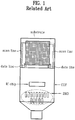
- FIG. 1 illustrates a diagram of a display device using a COF according to a related art.
- data lines are connected straight to a chip on film(hereinafter abbreviated COF) from a display panel.
- COF chip on film
- scan lines which are arranged on left and right sides of the display panel respectively, extend from the display panel with forming a curve so as to be coupled with the COF.
- the scan lines forming curves from both sides of the display panel extend longer than the data lines. Such a structure results in increasing line resistance of the scan lines and further delays a signal response.
- the line-resistance of the scan lines has a close relation -to the driving voltage of the display devices.
- the line resistance of the scan lines increases, the driving voltage thereof increases as well.
- the line resistance of the display device having a low driving voltage is a major issue.
- WO 98/33163 A shows a method for manufacturing a liquid crystal display module in which an IC is placed on a surface of a substrate so that the external connections of the IC electrically contact the desired interconnections on the substrate.
- the IC is connected with the LCD cell via connections.
- the LCD cell includes a first and second substrate, wherein the first substrate includes row conductors and the second substrate includes column conductors.
- US 6,066,916 A describes a electroluminescent matrix display device having a substrate, including a plurality of scanning electrodes and data electrodes.
- EP0617308 shows a display device including a display panel and a COF, the scanning and data line connection lines on the connection part of the COF extending perpendicular to each other.
- the present invention is directed to a display device using a COF that substantially obviates one or more problems due to limitations and disadvantages of the related art.
- An object of the present invention is to provide a display device using a COF enabling to reduce line resistance of scan and data lines in a display device.
- the object is solved by the features of the independent claims.
- the display using a COF a display device using a COF includes a display panel, a COF having a connection part on which the display channel is placed and a chip part on which a chip is placed, data and scan lines extending from the display panel, scan line connection lines on the connection part, the scan line connection lines connecting the scan lines electrically to the COF, and data line connection lines on the connection part, the data line connection lines connecting the data lines electrically to the COF, wherein the scan lines are directly connected to the chip on a first line in parallel with an extending line from the COF through the scan line connection lines formed on the COF at both sides of the display panel according to claims 1 to 3.
- a substrate material of the COF is one of glass and plastic.
- the scan line connection lines extend straightly on the first line and the data line connection lines form a curve with a predetermined angle so as to extend from the first line to the second line.
- the predetermined angle is 90° .
- FIG. 2 illustrates a diagram of a display device using a COF.
- a display device includes a display panel 30, a COF 80 having a connection part 20 on which the display panel 30 is placed and a chip part 10 on which a driving chip 60 is placed, and data and scan lines 40 and 50 extending from the- display panel 30 respectively.
- a reference numeral '70' indicates SMD parts.
- the scan lines 50 are connected straight to the COF 80 from the display panel 30 toward the IC(integrated circuits) chip 60 for driving (hereinafter abbreviated chip) a display device. Forming curves from the display panel 30 toward the chip 60, the data lines 40 are connected to the COF 80. And, a substrate material of the COF 80 is glass or plastic.
- the scan and data lines 50 and 40 extend from the display panel 30 attached to the glass or plastic as the substrate material of the COF 80.
- the driving chip 60 drives the display panel 30.
- the length of the scan lines between the display panel 30 and COF 80 is short as the scan lines 50 are straightly connected to the COF 80.
- the other length between the data lines 40 and COF 80 is relatively long.
- an IC chip for driving a current driving type display device uses a constant-current power supply, whereby a resistance value of data lines has less influence on a driving voltage of the display device.
- the scan lines 50 of the display panel 30 which are connected to a connection line(not shown in the drawing) are shorter than the data lines 40 connected to the other connection line(not shown in the drawing) of the COF 80 so as to be connected to the COF 80.
- the line resistance of the scan lines 50 in the display device is reduced.
- the IC chip 60 includes a constant-current power supply supplying the display device with a constant current.
- the display device includes EL(electro-luminescence), LED(light emitting diode), FED(field emission display) and the like.
- a width of the COF 80 is equal to or shorter than that of the display panel 30.
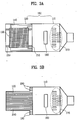
- FIG. 3A illustrates a diagram of a COF type display device according to a first embodiment of the present invention
- FIG. 3B illustrates a diagram of a COF structure according to the first embodiment of the present invention.
- a display device includes a display panel 130, a COF 180 having a connection part 120 on which the display panel 130 is placed and a chip part 110 on which a chip 160 is placed, and data and scan lines 140 and 150 extending from the display panel 130 respectively.
- the connection part 120 includes data line connection lines 190 and scan line connection lines 200.
- the scan line connection lines 200 are formed on the connection part 120 and connect the scan lines 150 electrically to the COF 180.
- the data line connection lines 190 are formed on the connection part 120 and connect the data lines 140-electrically to the COF 180.
- the scan lines 150 are straightly connected to the COF 180 through the scan line connection lines 200 at both sides of the display panel 130 on the first line in parallel with an extension line of the COF 180.
- the data lines 140 extend toward the chip 160 so as to be connected to the COF 180 through the data line connection-lines 190.
- the scan line connection lines 200 are straightly connected to the scan lines 150 at both sides of the display panel 130 corresponding to the first line, while the data line connection lines 190 are connected to the data lines 140 extending from both sides of the display panel 130 corresponding to the second line.
- the scan line connection lines 200 are longer than the data line connection lines 190.
- a resistance value of the scan lines depends on a metal inside the display device. If the resistance value is high, it is able to reduce a half of the resistance value of the scan lines 150 Using the COF 180 shown in FIG. 3B .
- the COF 180 shown in FIG. 3B includes the chip part 110 having the IC chip 160 and the SMD parts 170 and the connection part 120 to which the display panel 130 will be attached.
- connection part 120 On the connection part 120, the scan line connection lines 200, which will be connected to the scan lines 150 of the display device, are formed as long as a length of the connection part 120 in a direction of connecting the connection part 120 to the chip part 110.
- the data line connection lines 190 which will be connected to the data lines 140 of the display device, are formed so as to be much shorter than the scan line connection lines 200.
- connection part 120 of the COF 180 is simultaneously connected to both sides of the display panel 130 on the first line.
- a portion of the scan lines 150 starting from the display panel 130 is connected to one end of the connection part 120 far from the chip part 110, while the other portion of the scan lines 150 starting from the display panel 130 is connected to the other end of the connection part 120 adjacent to the chip part 110.
- the scan lines 150 of the display device are connected to the COF 180 at both sides of the display panel- 130, thereby enabling to reduce the resistance value of the scan lines 150.
- the display device uses the scan driving IC chip 160, as shown in FIG. 3A , whereby both sides of the display panel 130 corresponding to the first line are able to be simultaneously connected to the chip 160. Therefore, the display panel 130 is driven faster.
- FIG. 4A illustrates a diagram of a display device using a COF according to a second embodiment of the present invention
- FIG. 4B illustrates a diagram of a COF structure according to the second embodiment of the present invention.
- a display device includes a display panel 230, a COF 280 having a connection part 220 on which the display panel 230 is placed and a chip part 210 on which a chip 260 is placed, and data and scan lines 240 and 250 extending from the display panel 230 respectively.
- connection part 220 includes data line connection lines 290 and scan line connection lines 300.
- the scan line connection lines 300 are formed on the connection part 220 -and connect the scan lines 250 electrically to the COF 280.
- the data line connection lines 290 are formed on the connection part 220 and connect the data lines 240 electrically to the COF 280.
- the scan lines 250 are straightly connected to the COF 280 through the scan line connection lines 300 at both sides of the display panel 230 on a first line in parallel with a direction extending from the COF 280. And, forming curves from both sides of the display panel 230 corresponding to a second line perpendicular to the extending direction of the COF 280, a portion 240a of the data lines 240 extends toward the chip 260 so as to be connected to the COF 280 through the data line connection lines 290.
- the other portion 240b of the data lines 240 extend in a direction opposite to the chip 260 so as to be connected to the COF 280 through the data line connection lines 290.
- the COF 280 is constructed with the connection part 220 on which the display panel 230 is placed and the chip part 210 on which the chip 260 is placed.
- the connection part 220 includes the scan line connection lines 300 extending on the first line and the data line connection lines 290 also extending on the first line.
- the scan line connection lines 300 are straightly connected to the scan lines 250 at both sides of the display panel 230 corresponding to the first line, while the data line connection lines 290 are connected to the data lines 240 extending from both sides of the display panel 230 corresponding to the second line.
- the scan line connection lines 300 are longer than the data line connection lines 290.
- the scan line connection lines 300 and data line connection lines 290b which will be connected to the scan lines 250 starting from the display panel 230 and to the data lines 240b respectively, as shown in FIG. 4B , are formed to the extent of the length of the connection part 220. Yet, the data line connection lines 290a, which will be connected to the data lines 240a, are formed much shorter than the connection part 220.
- connection part 220 is connected to both sides of the display panel 230 on the first line simultaneously.
- the scan line connection lines 300 are formed on the substrate so that the scan lines 250 are connected to the connection part 220.
- the data line connection lines 290a and 290b are formed so as to connect the data lines 240a and 240b separated to extend from both sides of the display panel on the second line to the COF 280.
- the data lines 240a and 240b split to start from both sides of the display panel 230 as well, thereby enabling to reduce half of the resistance value of the data lines 240 as well as half of the resistance value of the scan lines 250.
- FIG. 5A illustrates a diagram of a display device using a COF according to a third embodiment of the present invention
- FIG. 5B illustrates a diagram of a COF structure according to the third embodiment of the present invention.
- a display device includes a display panel 330, a COF 380 having a connection part 320 on which the display panel 330 is placed and a chip part 310 on which a chip 360 is placed, and data and scan lines 340 and 350 extending from the display panel 330 respectively.
- connection part 320 includes data line connection lines 390 and scan line connection lines 400.
- the scan line connection lines 400 are formed on the connection part 320 and connect the scan lines 350 electrically to the COF 380.
- the data line connection lines 390 are formed on the connection part 320 and connect the data lines 340 electrically to the COF 380.
- the scan lines 350 are straightly connected to the COF 380 toward the chip 360 through the scan line connection lines 400 at both sides of the display panel 330 on a first line in parallel with a direction extending from the COF 380.
- the data lines 340 are connected to the COF 380 through the data line connection lines 390 from both sides of the display panel 330 on a second line perpendicular to the extending direction of the COF 380.
- the COF 380 is constructed with the connection part 320 on which the display panel 330 is placed and the chip part 310 on which the chip 360 is placed.
- connection part 320 formed are the scan line connection lines 400 extending straightly on the first line and the data line connection lines 390 forming a curve with a predetermined angle so as to extend from the first line to the second line.
- the predetermined angle in FIG. 5B is 90°.
- the scan line connection lines 400 are formed so that the scan lines 350 are connected directly to the COF 380 on the first line.
- the data line connection lines 390 are formed so that the data lines 340 are directly connected to the COF 380 on the second line.
- the data lines 340 are arranged in a direction forming a right angle with the scan lines 350.
- the data lines 340 are arranged as a straight-line form like the scan lines 350. And, the COF 380 shown in FIG. 5B is used. Therefore, the resistance value of the data lines 340 as well as that of the scan lines 350 is reduced.
- the COF 380 includes the chip part 310 having the IC chip 360 and an SMD part 370 and the connection part 320 having the scan and data Line connection lines 400 and 390 which connect the scan and data lines 350 and 340 starting from the display panel 330 to the COF 380 respectively.
- the scan line connection lines 400 as shown in FIG. 5B , having the longest length of the connection part 320 in order to connect the scan lines 350 to the COF 380 are formed on the connection part 320 in a direction of the first line.
- the data line connection lines 390 which will be connected to the data lines 340, are arranged in a direction so as to be bent with a predetermined angle from the first line to the second line.
- the bending angle in FIG-. 5B is 90°.
- the structures of the display device according to the embodiments of the present invention enable to reduce the resistance of the scan and data lines starting from the display panel and further decrease the driving voltage of the display device.
Landscapes
- Physics & Mathematics (AREA)
- Engineering & Computer Science (AREA)
- General Physics & Mathematics (AREA)
- Nonlinear Science (AREA)
- Computer Hardware Design (AREA)
- Theoretical Computer Science (AREA)
- Chemical & Material Sciences (AREA)
- Crystallography & Structural Chemistry (AREA)
- Mathematical Physics (AREA)
- Optics & Photonics (AREA)
- Devices For Indicating Variable Information By Combining Individual Elements (AREA)
- Electroluminescent Light Sources (AREA)
- Control Of Indicators Other Than Cathode Ray Tubes (AREA)
Claims (6)
- Anzeigevorrichtung, aufweisend:ein Anzeigefeld (130) mit vier verschiedenen Seiten;einen COF (Chip auf Film 180) mit einem Verbindungsteil (120), auf dem das Anzeigefeld (130) angeordnet ist, und einem Chipteil (110), auf dem ein Chip (160) angeordnet ist;Abtastleitungen (150), die sich von einer ersten und einer dritten Seite des Anzeigefelds (130) erstrecken, wobei die erste Seite dem Chipteil (110) zugewandt ist, die dritte Seite weit vom Chipteil (110) entfernt ist, die erste und die dritte Seite einander entgegengesetzt sind, die Abtastleitungen (150) sich geradlinig erstrecken,Datenleitungen (140), die sich von einer zweiten und vierten Seite des Anzeigefelds (130) erstrecken,wobei die zweite und die vierte Seite einander entgegengesetzt sind, die Datenleitungen (140) in Richtung des Chipteils (110) gekrümmt sind,Abtastleitungsverbindungsleitungen (200) auf dem Verbindungsteil (120) zum elektrischen Verbinden der Abtastleitungen (150) mit dem COF (180),Datenleitungsverbindungsleitungen (190) auf dem Verbindungsteil (120) zum elektrischen Verbinden der Datenleitungen (140) mit dem COF (180), wobei die Datenleitungsverbindungsleitungen (190) benachbart zu den Abtastleitungsverbindungsleitungen (200) auf dem Verbindungsteil (120) gebildet sind,wobei die Abtastleitungen (150) mit dem Chip (160) auf einer ersten Linie parallel zu einer Erstreckungslinie des COF (180) verbunden sind, durch die Abtastleitungsverbindungsleitungen (200), die entsprechend der ersten Leitung geradlinig gebildet sind,wobei die Abtastleitungsverbindungsleitungen (200) mit Abtastleitungen (150) auf der ersten und der dritten Seite des Anzeigefelds (130) verbunden sind und die Datenleitungsverbindungsleitungen (190) mit den gekrümmten Datenleitungen (140) verbunden sind,wobei die Datenleitungsverbindungsleitungen (190) kürzer sind als die Abtastleitungsverbindungsleitungen (200).
- Anzeigevorrichtung, aufweisend:ein Anzeigefeld (230) mit vier verschiedenen Seiten;einen COF (Chip auf Film 280) mit einem Verbindungsteil (220), auf dem das Anzeigefeld (230) angeordnet ist, und einem Chipteil (210), auf dem ein Chip (260) angeordnet ist;Abtastleitungen (250), die sich von einer ersten und einer dritten Seite des Anzeigefelds (230) erstrecken, wobei die erste Seite dem Chipteil (210) zugewandt ist, die dritte Seite weit von dem Chipteil (210) entfernt ist, die erste und die dritte Seite einander entgegengesetzt sind, die Abtastleitungen (250) sich geradlinig erstrecken,Datenleitungen (240a, 240b), die sich von einer zweiten und einer vierten Seite des Anzeigefelds (230) erstrecken, wobei die zweite und die vierte Seite einander entgegengesetzt sind, die Datenleitungen (240a, 240b) auf der zweiten und vierten Seite des Anzeigefelds (230) geteilt sind, so dass ein Teil in Richtung des Chipteils (210) gekrümmt ist und ein zweiter Teil in einer Richtung von dem Chipteil (210) weg gekrümmt ist,Abtastleitungsverbindungsleitungen (300) auf dem Verbindungsteil (220) zum elektrischen Verbinden der Abtastleitungen (250) mit dem COF (280),Datenleitungsverbindungsleitungen (290a, 290b) auf dem Verbindungsteil (220) zum elektrischen Verbinden der Datenleitungen (240a, 240b) mit dem COF (280),wobei die Datenleitungsverbindungsleitungen (290a, 290b) benachbart zu den Abtastleitungsverbindungsleitungen (300) auf dem Verbindungsteil (220) gebildet sind,wobei die Abtastleitungen (250) mit dem Chip (260) auf einer ersten Linie parallel zu einer Erstreckungslinie des COF (280) verbunden sind, durch die Abtastleitungsverbindungsleitungen (300), die entsprechend der ersten Leitung geradlinig gebildet sind,wobei die Abtastleitungsverbindungsleitungen (300) mit Abtastleitungen (250) auf der ersten und der dritten Seite des Anzeigefelds (230) verbunden sind und die Datenleitungsverbindungsleitungen (290a, 290b) mit den gekrümmten Datenleitungen (240a, 240b) verbunden sind,die Datenleitungsverbindungsleitungen (290a), die mit den Datenleitungen (240a) verbunden sind, die in Richtung des Chipteils (210) gekrümmt sind, kürzer sind als die Abtastleitungsverbindungsleitungen (300) und Datenleitungsverbindungsleitungen (290b), die mit den Datenleitungen (240b) verbundenen sind, die von dem Chipteil (210) weg gekrümmt sind.
- Anzeigevorrichtung, aufweisend:ein Anzeigefeld (330) mit vier verschiedenen Seiten;ein COF (Chip auf Film 380) mit einem Verbindungsteil (320), auf dem das Anzeigefeld (330) angeordnet ist, und einem Chipteil (310), auf dem ein Chip (360) platziert ist;Abtastleitungen (350), die sich von einer ersten und einer dritten Seite des Anzeigefelds (330) erstrecken, wobei die erste Seite dem Chipteil (310) zugewandt ist, die dritte Seite weit von dem Chipteil (310) entfernt ist, die erste und die dritte Seite einander entgegengesetzt sind, die Abtastleitungen (350) geradlinig verlaufen,Datenleitungen (340), die sich von einer zweiten und vierten Seite des Anzeigefelds (230) erstrecken,wobei die zweite und die vierte Seite einander entgegengesetzt sind, die Datenleitungen (340) geradlinig verlaufen,Abtastleitungsverbindungsleitungen (400) auf dem Verbindungsteil (320) zum elektrischen Verbinden der Abtastleitungen (350) mit dem COF (380),Datenleitungsverbindungsleitungen (390) auf dem Verbindungsteil (320) zum elektrischen Verbinden der Datenleitungen (340) mit dem COF (380), wobei die Datenleitungsverbindungsleitungen (390) benachbart zu den Abtastleitungsverbindungsleitungen (390) auf dem Verbindungsteil (320) gebildet sind, die Datenleitungsverbindungsleitungen (390) gekrümmt sind, so dass ein Teil einer Datenleitungsverbindungsleitung sich parallel zu undein anderer Teil senkrecht zu einer ersten Linie parallel zu einer Erstreckungslinie des COF (380) erstreckt,wobei die Abtastleitungen (350) entsprechend der ersten Leitung geradlinig gebildet sind und auf der ersten Linie mit dem Chip (360) durch die Abtastleitungsverbindungsleitungen (400) verbunden sind, die auf dem COF (380) auf der ersten und der dritten Seite des Anzeigefelds (330) gebildet sind, unddie gekrümmten Datenleitungsverbindungsleitungen (390) mit den Datenleitungen (340) auf der zweiten und der vierten Seite des Anzeigefelds (330) verbunden sind.
- Anzeigevorrichtung nach Anspruch 1, 2 oder 3, wobei der Chip (160, 260, 360) ein Abtasttreiberchip ist, der das Anzeigefeld (130, 230, 330) treibt.
- Anzeigevorrichtung nach einem der vorhergehenden Ansprüche, wobei ein Substratmaterial des COF (180, 280, 380) eines von Glas und Kunststoff ist.
- Anzeigevorrichtung nach einem der vorhergehenden Ansprüche, wobei die Anzeigevorrichtung EL (Elektrolumineszenz), LED (Leuchtdiode), FED (Feldemissionsanzeige) aufweist.
Applications Claiming Priority (2)
| Application Number | Priority Date | Filing Date | Title |
|---|---|---|---|
| KR1020000058786A KR20020027958A (ko) | 2000-10-06 | 2000-10-06 | 표시소자의 cof 구조 |
| KR2000058786 | 2000-10-06 |
Publications (3)
| Publication Number | Publication Date |
|---|---|
| EP1195818A2 EP1195818A2 (de) | 2002-04-10 |
| EP1195818A3 EP1195818A3 (de) | 2007-11-07 |
| EP1195818B1 true EP1195818B1 (de) | 2018-01-10 |
Family
ID=19692174
Family Applications (1)
| Application Number | Title | Priority Date | Filing Date |
|---|---|---|---|
| EP01123771.6A Expired - Lifetime EP1195818B1 (de) | 2000-10-06 | 2001-10-04 | COF-verwendende Anzeigevorrichtung |
Country Status (4)
| Country | Link |
|---|---|
| US (1) | US6738030B2 (de) |
| EP (1) | EP1195818B1 (de) |
| KR (1) | KR20020027958A (de) |
| CN (1) | CN1165032C (de) |
Families Citing this family (18)
| Publication number | Priority date | Publication date | Assignee | Title |
|---|---|---|---|---|
| KR20040003599A (ko) * | 2002-07-03 | 2004-01-13 | 주식회사 엘리아테크 | 유기 전계 발광 패널의 모듈 |
| JP3977299B2 (ja) * | 2002-09-18 | 2007-09-19 | セイコーエプソン株式会社 | 電気光学装置、マトリクス基板、及び電子機器 |
| TWI362231B (en) * | 2003-11-21 | 2012-04-11 | Semiconductor Energy Lab | Display device |
| KR101034748B1 (ko) * | 2004-12-31 | 2011-05-17 | 엘지디스플레이 주식회사 | 액정패널 및 이를 구비한 액정표시장치 |
| TW200634375A (en) * | 2005-03-28 | 2006-10-01 | Elan Microelectronics Corp | Power line structure for liquid crystal display panel |
| KR100775827B1 (ko) * | 2005-12-22 | 2007-11-13 | 엘지전자 주식회사 | 균일한 저항값을 갖는 스캔 라인을 포함한 유기 전계 발광소자 |
| RU2390046C1 (ru) * | 2009-02-17 | 2010-05-20 | Открытое акционерное общество "Научно-производственный комплекс "ЭЛАРА" имени Г.А. Ильенко" (ОАО "ЭЛАРА") | Модуль дисплея (варианты) |
| US20110254758A1 (en) * | 2010-04-19 | 2011-10-20 | Qualcomm Mems Technologies, Inc. | Flex Design and Attach Method for Reducing Display Panel Periphery |
| US20120092294A1 (en) | 2010-10-18 | 2012-04-19 | Qualcomm Mems Technologies, Inc. | Combination touch, handwriting and fingerprint sensor |
| CN102509723B (zh) * | 2011-10-18 | 2014-05-21 | 深圳市华星光电技术有限公司 | 覆晶薄膜的面板结构 |
| US9281672B2 (en) * | 2012-01-20 | 2016-03-08 | Sage Electrochromics, Inc. | Electrical connectivity within architectural glazing frame systems |
| US9024910B2 (en) | 2012-04-23 | 2015-05-05 | Qualcomm Mems Technologies, Inc. | Touchscreen with bridged force-sensitive resistors |
| KR102085274B1 (ko) * | 2013-06-21 | 2020-03-06 | 삼성디스플레이 주식회사 | 유기 발광 표시 장치 |
| CN103558703B (zh) * | 2013-10-12 | 2016-08-10 | 深圳市华星光电技术有限公司 | 超窄边框液晶显示器及其驱动电路的cof封装结构 |
| KR102305920B1 (ko) | 2015-04-30 | 2021-09-28 | 삼성디스플레이 주식회사 | 유기 발광 표시 장치 |
| CN111527536A (zh) | 2017-11-24 | 2020-08-11 | 华为技术有限公司 | 显示装置及其相关集成电路、方法和用户设备 |
| RU184564U1 (ru) * | 2018-07-12 | 2018-10-30 | Акционерное общество "Промышленная группа "Метран" (АО "ПГ "Метран") | Детектор электромагнитной помехи, воздействующей на модуль жки |
| US11798876B2 (en) | 2021-09-07 | 2023-10-24 | Novatek Microelectronics Corp. | Chip on film package and display device including the same |
Citations (2)
| Publication number | Priority date | Publication date | Assignee | Title |
|---|---|---|---|---|
| EP0617308A1 (de) * | 1993-03-22 | 1994-09-28 | NCR International, Inc. | Flüssigkristallanzeige mit integrierter Elektronik |
| US6066916A (en) * | 1996-08-19 | 2000-05-23 | Denso Corporation | Electroluminescent matrix display device |
Family Cites Families (7)
| Publication number | Priority date | Publication date | Assignee | Title |
|---|---|---|---|---|
| JPH05232512A (ja) * | 1992-02-25 | 1993-09-10 | Sanyo Electric Co Ltd | 液晶表示装置 |
| JP3141312B2 (ja) * | 1992-12-21 | 2001-03-05 | キヤノン株式会社 | 表示素子 |
| US5923119A (en) * | 1996-05-20 | 1999-07-13 | Matsushita Electric Industrial Co., Ltd. | Organic thin-film electroluminescent display device, method for driving the same and method for fabricating the same |
| WO1998033163A1 (en) * | 1997-01-27 | 1998-07-30 | Koninklijke Philips Electronics N.V. | Method of manufacturing a liquid crystal display module |
| CN1169226C (zh) * | 1997-06-11 | 2004-09-29 | 精工爱普生株式会社 | 半导体装置和液晶显示装置以及含有它们的电子机器 |
| JP2000259091A (ja) * | 1999-03-04 | 2000-09-22 | Casio Comput Co Ltd | 表示パネル、フレキシブル配線基板及びそれらを備えた表示装置 |
| JP2001034237A (ja) * | 1999-07-21 | 2001-02-09 | Fujitsu Ltd | 液晶表示装置 |
-
2000
- 2000-10-06 KR KR1020000058786A patent/KR20020027958A/ko not_active Ceased
-
2001
- 2001-10-04 EP EP01123771.6A patent/EP1195818B1/de not_active Expired - Lifetime
- 2001-10-04 US US09/969,613 patent/US6738030B2/en not_active Expired - Lifetime
- 2001-10-06 CN CNB011380004A patent/CN1165032C/zh not_active Expired - Lifetime
Patent Citations (2)
| Publication number | Priority date | Publication date | Assignee | Title |
|---|---|---|---|---|
| EP0617308A1 (de) * | 1993-03-22 | 1994-09-28 | NCR International, Inc. | Flüssigkristallanzeige mit integrierter Elektronik |
| US6066916A (en) * | 1996-08-19 | 2000-05-23 | Denso Corporation | Electroluminescent matrix display device |
Also Published As
| Publication number | Publication date |
|---|---|
| US6738030B2 (en) | 2004-05-18 |
| CN1165032C (zh) | 2004-09-01 |
| CN1348162A (zh) | 2002-05-08 |
| EP1195818A3 (de) | 2007-11-07 |
| EP1195818A2 (de) | 2002-04-10 |
| KR20020027958A (ko) | 2002-04-15 |
| US20020041146A1 (en) | 2002-04-11 |
Similar Documents
| Publication | Publication Date | Title |
|---|---|---|
| EP3261142B1 (de) | Anzeigevorrichtung mit einem biegebereich | |
| US6738030B2 (en) | Display device using COF | |
| US7306357B2 (en) | Line light source using light emitting diode and lens and backlight unit using the same | |
| US20080048948A1 (en) | Display device, flexible member, and method thereof | |
| CN100582885C (zh) | 显示设备 | |
| JP2006113587A (ja) | 発光表示装置 | |
| EP1742522A2 (de) | Diodenmodul für Beleuchtungsanordnung, Rückbeleuchtungsanordnung und Anzeigevorrichtung damit | |
| CN112447144A (zh) | 发光设备和具有其的显示设备 | |
| KR101293949B1 (ko) | 백라이트 어셈블리 및 이를 갖는 표시장치 | |
| CN111009755B (zh) | 连接器组件和具有该连接器组件的显示设备 | |
| KR100571218B1 (ko) | 접속 부재 및 플라즈마 디스플레이 패널 구동 장치 | |
| CN103857185B (zh) | 印刷电路板以及包括该印刷电路板的发光器件和背光单元 | |
| JP2001117093A (ja) | Lcdバックライト | |
| KR102887784B1 (ko) | 디스플레이 장치 및 이의 제조방법 | |
| JP2002231033A (ja) | 表示装置のバックライト取付構造 | |
| JP6771515B2 (ja) | 回路基板及び表示装置 | |
| EP2487534A2 (de) | Rückbeleuchtungseinheit | |
| KR102871634B1 (ko) | 디스플레이 디바이스 | |
| US20250275324A1 (en) | Display device in which pad electrodes of a circuit board and pad electrodes of a display panel are aligned and a method for fabricating the same | |
| KR100739292B1 (ko) | 유기 발광 표시장치 | |
| CN114373421B (zh) | 显示面板和显示装置 | |
| KR20160061153A (ko) | 반도체 발광 소자를 이용한 디스플레이 장치 | |
| JP2005309193A (ja) | 表示装置 | |
| US20250355297A1 (en) | Display device | |
| KR200173165Y1 (ko) | 평판표시소자의 접속구조 |
Legal Events
| Date | Code | Title | Description |
|---|---|---|---|
| PUAI | Public reference made under article 153(3) epc to a published international application that has entered the european phase |
Free format text: ORIGINAL CODE: 0009012 |
|
| AK | Designated contracting states |
Kind code of ref document: A2 Designated state(s): AT BE CH CY DE DK ES FI FR GB GR IE IT LI LU MC NL PT SE TR |
|
| AX | Request for extension of the european patent |
Free format text: AL;LT;LV;MK;RO;SI |
|
| PUAL | Search report despatched |
Free format text: ORIGINAL CODE: 0009013 |
|
| AK | Designated contracting states |
Kind code of ref document: A3 Designated state(s): AT BE CH CY DE DK ES FI FR GB GR IE IT LI LU MC NL PT SE TR |
|
| AX | Request for extension of the european patent |
Extension state: AL LT LV MK RO SI |
|
| RIC1 | Information provided on ipc code assigned before grant |
Ipc: H01L 27/15 20060101ALI20071001BHEP Ipc: H01L 27/00 20060101ALI20071001BHEP Ipc: G02F 1/13 20060101AFI20071001BHEP |
|
| 17P | Request for examination filed |
Effective date: 20080502 |
|
| RAP1 | Party data changed (applicant data changed or rights of an application transferred) |
Owner name: LG DISPLAY CO., LTD. |
|
| AKX | Designation fees paid |
Designated state(s): AT DE FR GB IT |
|
| 17Q | First examination report despatched |
Effective date: 20080623 |
|
| GRAP | Despatch of communication of intention to grant a patent |
Free format text: ORIGINAL CODE: EPIDOSNIGR1 |
|
| RIC1 | Information provided on ipc code assigned before grant |
Ipc: H01L 51/52 20060101AFI20170424BHEP Ipc: H01L 27/32 20060101ALI20170424BHEP Ipc: G02F 1/13 20060101ALI20170424BHEP Ipc: H05K 1/18 20060101ALN20170424BHEP |
|
| INTG | Intention to grant announced |
Effective date: 20170529 |
|
| RIN1 | Information on inventor provided before grant (corrected) |
Inventor name: KIM, HAK SU Inventor name: KIM, JUNG BAE |
|
| GRAJ | Information related to disapproval of communication of intention to grant by the applicant or resumption of examination proceedings by the epo deleted |
Free format text: ORIGINAL CODE: EPIDOSDIGR1 |
|
| REG | Reference to a national code |
Ref country code: DE Ref legal event code: R079 Ref document number: 60150740 Country of ref document: DE Free format text: PREVIOUS MAIN CLASS: H01L0027150000 Ipc: H01L0051520000 |
|
| GRAP | Despatch of communication of intention to grant a patent |
Free format text: ORIGINAL CODE: EPIDOSNIGR1 |
|
| INTC | Intention to grant announced (deleted) | ||
| RIC1 | Information provided on ipc code assigned before grant |
Ipc: G02F 1/13 20060101ALI20170707BHEP Ipc: H01L 51/52 20060101AFI20170707BHEP Ipc: H01L 27/32 20060101ALI20170707BHEP Ipc: H05K 1/18 20060101ALN20170707BHEP |
|
| INTG | Intention to grant announced |
Effective date: 20170803 |
|
| RAP1 | Party data changed (applicant data changed or rights of an application transferred) |
Owner name: LG DISPLAY CO., LTD. |
|
| GRAS | Grant fee paid |
Free format text: ORIGINAL CODE: EPIDOSNIGR3 |
|
| GRAA | (expected) grant |
Free format text: ORIGINAL CODE: 0009210 |
|
| AK | Designated contracting states |
Kind code of ref document: B1 Designated state(s): AT DE FR GB IT |
|
| REG | Reference to a national code |
Ref country code: GB Ref legal event code: FG4D |
|
| REG | Reference to a national code |
Ref country code: AT Ref legal event code: REF Ref document number: 963317 Country of ref document: AT Kind code of ref document: T Effective date: 20180115 |
|
| REG | Reference to a national code |
Ref country code: DE Ref legal event code: R096 Ref document number: 60150740 Country of ref document: DE |
|
| REG | Reference to a national code |
Ref country code: AT Ref legal event code: MK05 Ref document number: 963317 Country of ref document: AT Kind code of ref document: T Effective date: 20180110 |
|
| REG | Reference to a national code |
Ref country code: FR Ref legal event code: PLFP Year of fee payment: 18 |
|
| PG25 | Lapsed in a contracting state [announced via postgrant information from national office to epo] |
Ref country code: AT Free format text: LAPSE BECAUSE OF FAILURE TO SUBMIT A TRANSLATION OF THE DESCRIPTION OR TO PAY THE FEE WITHIN THE PRESCRIBED TIME-LIMIT Effective date: 20180110 |
|
| REG | Reference to a national code |
Ref country code: DE Ref legal event code: R097 Ref document number: 60150740 Country of ref document: DE |
|
| PG25 | Lapsed in a contracting state [announced via postgrant information from national office to epo] |
Ref country code: IT Free format text: LAPSE BECAUSE OF FAILURE TO SUBMIT A TRANSLATION OF THE DESCRIPTION OR TO PAY THE FEE WITHIN THE PRESCRIBED TIME-LIMIT Effective date: 20180110 |
|
| PLBE | No opposition filed within time limit |
Free format text: ORIGINAL CODE: 0009261 |
|
| STAA | Information on the status of an ep patent application or granted ep patent |
Free format text: STATUS: NO OPPOSITION FILED WITHIN TIME LIMIT |
|
| 26N | No opposition filed |
Effective date: 20181011 |
|
| PGFP | Annual fee paid to national office [announced via postgrant information from national office to epo] |
Ref country code: FR Payment date: 20200824 Year of fee payment: 20 Ref country code: GB Payment date: 20200824 Year of fee payment: 20 |
|
| PGFP | Annual fee paid to national office [announced via postgrant information from national office to epo] |
Ref country code: DE Payment date: 20200820 Year of fee payment: 20 |
|
| REG | Reference to a national code |
Ref country code: DE Ref legal event code: R071 Ref document number: 60150740 Country of ref document: DE |
|
| REG | Reference to a national code |
Ref country code: GB Ref legal event code: PE20 Expiry date: 20211003 |
|
| PG25 | Lapsed in a contracting state [announced via postgrant information from national office to epo] |
Ref country code: GB Free format text: LAPSE BECAUSE OF EXPIRATION OF PROTECTION Effective date: 20211003 |