EP1193861A2 - Amplificateur à contre-réaction de type aval - Google Patents
Amplificateur à contre-réaction de type aval Download PDFInfo
- Publication number
- EP1193861A2 EP1193861A2 EP01122758A EP01122758A EP1193861A2 EP 1193861 A2 EP1193861 A2 EP 1193861A2 EP 01122758 A EP01122758 A EP 01122758A EP 01122758 A EP01122758 A EP 01122758A EP 1193861 A2 EP1193861 A2 EP 1193861A2
- Authority
- EP
- European Patent Office
- Prior art keywords
- signal
- power
- signal level
- output
- combiner
- Prior art date
- Legal status (The legal status is an assumption and is not a legal conclusion. Google has not performed a legal analysis and makes no representation as to the accuracy of the status listed.)
- Granted
Links
Images


Classifications
-
- H—ELECTRICITY
- H03—ELECTRONIC CIRCUITRY
- H03F—AMPLIFIERS
- H03F1/00—Details of amplifiers with only discharge tubes, only semiconductor devices or only unspecified devices as amplifying elements
- H03F1/32—Modifications of amplifiers to reduce non-linear distortion
- H03F1/3223—Modifications of amplifiers to reduce non-linear distortion using feed-forward
- H03F1/3229—Modifications of amplifiers to reduce non-linear distortion using feed-forward using a loop for error extraction and another loop for error subtraction
-
- H—ELECTRICITY
- H03—ELECTRONIC CIRCUITRY
- H03F—AMPLIFIERS
- H03F2201/00—Indexing scheme relating to details of amplifiers with only discharge tubes, only semiconductor devices or only unspecified devices as amplifying elements covered by H03F1/00
- H03F2201/32—Indexing scheme relating to modifications of amplifiers to reduce non-linear distortion
- H03F2201/3218—Indexing scheme relating to modifications of amplifiers to reduce non-linear distortion the main amplifier or error amplifier being a feedforward amplifier
Definitions
- the invention relates to a feedforward amplifier and a communication equipment, which are primarily used for a base station device of mobile communication equipment.
- Fig. 12 shows an example of the configuration of a conventional feadforward amplifier.
- reference numeral 1 denotes an input terminal, 2 an output terminal, 3 and 8 power splitters, 4 and 9 power-combiners, 5 and 13 vector adjustors, 6 a main amplifier, 7 and 10 delay circuits, and 14 an error amplifier, respectively.
- symbols a to k and m added to the power splitters 3 and 8 and the power-combiners 4 and 9 show respective ports.
- an input signal input from the input terminal 1 and including a plurality of carrier frequency components is split into two parts by the power splitter 3, and the two parts are output from the port b and port c respectively.
- the signal output from the port b is amplified by the main amplifier 6 through the vector adjustor 5, and then passes through the power splitter 8 and the delay circuit 10, inputting into the port j of the power-combiner 4.
- the signal including distortion components caused by intermodulation due to non-linearity of the main amplifier 6 in addition to the carrier frequency components are input into the port j.
- part of the output signal of the main amplifier 6 is took out from a port f of the power splitter 8 and input into a port h of the power-combiner 9.
- the signal output from the port c inputs into a port g of the power-combiner 9 through the delay circuit 7.
- the vector adjustor 5 and delay circuit 7 are adjusted such that the carrier frequency components of the respective signals input into the port g and the port h may have the same amplitudes and opposite phases, thereby a signal having only the distortion components with the carrier frequency components canceled out being output from the port i.
- the signal output from the port i is amplified by the error amplifier 14 through the vector adjustor 13 and inputs into a port k of the power-combiner 4.
- the vector adjustor 13 and the delay circuit 10 are adjusted such that the distortion components of signals input into the port j and port k may have the same amplitudes and opposite phases, thereby a signal having only the carrier frequency components with the distortion components canceled out being output from a port m of the power-combiner 4 to the output terminal 2.
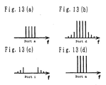
- Figs. 13 (a) to (d) shows frequency spectra of signals at the ports a, d, i and m.
- the frequency spectrum of the signal at the port a is composed of carrier frequency components .
- the frequency spectrum of the signal at the port d is composed of carrier frequency components and distortion components.
- the frequency spectrum of the signal at the port i is composed of only the distortion components with the carrier frequency components canceled out.
- the frequency spectrum of the signal from the port m is composed of only the carrier frequency components with the distortion components canceled out.
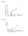
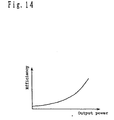
- Fig. 12 has a problem that a decrease in output power leads to a decrease in efficiency as shown in Fig. 14.
- the efficiency means the ratio of output power to consumption power.
- the invention has an object to provide a feedforward amplifier and a communication equipment of which efficiency does not decrease even in the event of the reduction of output power.
- the invention has another object to provide a feedforward amplifier and a communication equipment of which communication does not stop completely even in the event of the failure of the main amplifier.
- the 1st invention of the present invention is a feedforward amplifier comprising:
- the 2nd invention of the present invention is the feedforward amplifier according to 1st invention, further comprising:
- the 3rd invention of the present invention is the feedforward amplifier according to 1st invention, further comprising:
- the 4th invention of the present invention is the feedforward amplifier according to 1st invention, further comprising:
- the 5th invention of the present invention is the feedforward amplifier according to 1st invention, further comprising:
- the 6th invention of the present invention is the feedforward amplifier according to 1st invention, further comprising:
- the 7th invention of the present invention is the feedforward amplifier according to 4th or 5th inventions, wherein said distortion suppression power-combiner is a variable power-combiner that can have a tight coupling state and a loose coupling state, and when said first signal level is higher than a predetermined value, said control means controls said variable power-combiner to have said loose coupling state, and when said first signal level is not higher than the predetermined value, said control means controls said variable power-combiner to have said tight coupling state.
- said distortion suppression power-combiner is a variable power-combiner that can have a tight coupling state and a loose coupling state, and when said first signal level is higher than a predetermined value, said control means controls said variable power-combiner to have said loose coupling state, and when said first signal level is not higher than the predetermined value, said control means controls said variable power-combiner to have said tight coupling state.
- the 8th invention of the present invention is the feedforward amplifier according to 4th or 6th inventions, wherein said distortion suppression power-combiner is a variable power-combiner that can have a tight coupling state and a loose coupling state, when said first signal level is lower than a predetermined value, said control means controls said variable power-combiner to have said loose coupling state, and when said first signal level is not lower than the predetermined value, said control means controls said variable power-combiner to have said tight coupling state.
- said distortion suppression power-combiner is a variable power-combiner that can have a tight coupling state and a loose coupling state
- said control means controls said variable power-combiner to have said loose coupling state
- said control means controls said variable power-combiner to have said tight coupling state.
- the 9th invention of the present invention is the feedforward amplifier according to 4th or 5th inventions, wherein, when said first signal level is not higher than a predetermined value, said control means performs such control that the output signal of said error amplifier can be output without passing through said distortion suppression power-combiner.
- the 10th invention of the present invention is the feedforward amplifier according to 4th or 6th inventions, wherein, when said first signal level is not lower than a predetermined value, said control means performs such control that the output signal of said error amplifier can be output without passing through said distortion suppression power-combiner.
- the 11th invention of the present invention is the feedforward amplifier according to 1st invention, further comprising:
- the 12th invention of the present invention is the feedforward amplifier according to 1st invention, further comprising:
- the 13th invention of the present invention is the feedforward amplifier according to 1st invention, further comprising:
- the 14th invention of the present invention is the feedforward amplifier according to 1st invention, further comprising:
- the 15th invention of the present invention is the feedforward amplifier according to 1st invention, further comprising:
- the 16th invention of the present invention is the feedforward amplifier according to 1st invention, further comprising:
- the 17th invention of the present invention is the feedforward amplifier according to any one of 2nd, 4th, 5th, 11th, 13th, and 15th inventions; wherein said first signal level detection means is provided in an upstream stage of said first power splitter, or between said first power splitter and said first vector adjustor, or between said first vector adjustor and said main amplifier, or between said first power splitter and said first delay circuit, or between said first delay circuit and said distortion detection power-combiner, or at the input of said baseband signal generating portion, or at the output of said baseband signal generating portion, or in said baseband signal generating potion, or at the input of said transmitting circuit, or at the output of said transmitting circuit, or in said transmitting circuit.
- the 18th invention of the present invention is the feedback amplifier according to any one of 3rd, 4th, 6th, 12th, 14th, and 16th inventions, wherein said first signal level detection means is provided at the input of said receiving circuit, or at the output of said receiving circuit, or in said receiving circuit.
- the 19th invention of the present invention is the feedforward amplifier according to 4th ivnention, wherein said second signal level detection means is provided in a downstream stage of said distortion suppression power-combiner, or between said second power splitter and said second delay circuit, or between said second delay circuit and said distortion suppression power-combiner.
- the 20th invention of the present invention is the feedforward amplifier according to 17th ivention, wherein said first signal level is the signal level of said input signal, and when said first signal level detection means detects the signal level of said input signal,
- the 21st invention of the present invention is the feedforward amplifier according to 19th invention, wherein said second signal level detection means has a signal level detection power-splitter for splitting said output signal into two parts and detection means of detecting said signal level of one output signal of said signal level detection power-splitter, and the other output signal of said signal level detection power-splitter is supplied to a downstream stage.
- the 22nd invention of the present invention is the feedforward amplifier according to any one of 2nd, 3rd, 11th, 12th, 15th, and 16th inventions, wherein the stopping of the operation of said error amplifier is to perform such control that the power supply for said error amplifier can be turned off and/or to perform such control that the output signal of said second vector adjustor can not be input by said error amplifier.
- the 23rd invention of the present invention is the feedforward amplifier according to any one of 4th, 5th, 6th, 11th, 12th, 13th, 14th, 15th, and 16th inventions, wherein the stopping of the operation of said main amplifier is to perform such control that the power supply for said main amplifier can be turned off and/or to perform such control that the output signal of said first vector adjustor can not be input by said main amplifier.
- the 24th invention of the present invention is the feedforward amplifier according to any one of 13th, 14th, 15th, and 16th inventions, wherein the stopping of the operation of said second error amplifier is to perform such control that the power supply for said second error amplifier can be turned off and/or to perform such control that the output signal of said third vector adjustor can not be input by said secondary error amplifier.
- the 25th invention of the present invention is a communication equipment comprising:
- the error amplifier can be used to amplify and output the input signal, thereby allowing the improved reliability of the feedforward amplifier.
- equipping communication equipments such as mobile communication equipments with the feedforward amplifier according to the invention allows the higher efficiency and improved reliability of communication equipments such as mobile communication equipments.
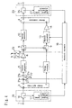
- Fig. 1 shows a configuration diagram of the feedforward amplifier according to the embodiment 1 of the invention.
- reference numeral 11 denotes a switch circuit, 12 a terminating resistor, 15 an error amplifier power switch, 16 a power splitter, 17 a signal level detection circuit, and 18 a control circuit for switching the switch circuit 11 and the error amplifier power switch circuit 15 depending on the signal level detected by the signal level detection circuit 17, respectively.
- the power splitter 16 and the signal level detection circuit 17 constitute a signal level detection portion 19. Further, a symbol n added to the power splitter 16 shows a port.
- the power splitter 3 of the present embodiment is an example of the first power splitter of the invention
- the vector adjustor 5 an example of the first vector adjustor
- the power splitter 8 an example of the second power splitter
- the delay circuit 7 an example of the first delay circuit
- the power-combiner 9 an example of the distortion detection power-combiner
- the delay circuit 10 an example of the second delay circuit
- the vector adjustor 13 an example of the second vector adjustor
- the power-combiner 4 an example of the distortion suppression power-combiner
- the control circuit 18 an example of the control means
- the signal level detection portion 19 an example of the first signal level detection means
- An input signal input from an input terminal 1 and including a plurality of carrier frequency components is input into a port a of the power splitter 3 through the power splitter 16. Then, part of the input signal is took out from the port n of the power splitter 16 and input into the signal level detection circuit 17.
- the signal input into the port a of the power splitter 3 is split into two parts, which are output through a port b and port c respectively.
- the signal output from the port b is amplified by the main amplifier 6 through the vector adjustor 5 and then input into a port j of the power-combiner 4 through the power splitter 8 and the delay circuit 10. At this time, signals including distortion components caused by intermodulation due to the non-linearity of the main amplifier 6 in addition to the carrier frequency components are input into the port j.
- part of the output signal of the main amplifier 6 is took out from a port f of the power splitter 8 and input into a port h of the power-combiner 9.
- the signal output from the port c is input into a port g of the power-combiner 9 through the delay circuit 7.
- the vector adjustor 5 and the delay circuit 7 are adjusted such that the carrier frequency components of the signals input into the port g and the port h may have the same amplitudes and opposite phases, thereby a signal having only the distortion components with the carrier frequency components canceled out being output from the port i.
- the signal output from the port i is input into a common terminal 11a of the switch circuit 11.
- the control circuit 18 connects the common terminal 11a to an output switching terminal 11b of the switch circuit 11, and further turns on the error amplifier power switch circuit 15.
- the control circuit 18 connects the common terminal 11a to an output switching terminal 11c of the switch circuit 11 and further turns off the error amplifier power switch circuit 15.
- the signal input into the common terminal 11a of the switch circuit 11 is amplified by the error amplifier 14 through the output switching terminal 11b and the vector adjustor 13, and then input into a port k of the power-combiner 4.
- the vector adjustor 13 and the delay circuit 10 are adjusted such that the distortion components of the signals input into the port j and the port k may have the same amplitudes and opposite phases, thereby a signal having only the carrier frequency components with the distortion components canceled out being output from a port m of the power-combiner 4 into an output terminal 2.
- the level of distortions caused by the main amplifier 6 decreases as its output power decreases as shown in Fig. 2.
- D1 e.g. - 60 dBc
- P1 dBm
- the input signal level is used to switch the switch circuit 11 and the error amplifier power switch circuit 15, it is apparent that the same operation can be also obtained by switching them depending on the level of signals output from the port b of the power splitter 3, the vector adjustor 5, the port f of the power splitter 8, the port c of the power splitter 3, or the delay circuit 7.
- the signal level detection portion 19 should be inserted in the position for the signal level to be detected.
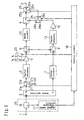
- Fig. 4 shows a configuration diagram of the feedforward amplifier according to the embodiment 2 of the invention.
- reference numeral 21 denotes a switch circuit, 22 a terminating resistor, 23 a main amplifier power-switch-circuit, 26 a power splitter, and 27 a signal level detection circuit, respectively.
- the power splitter 26 and the signal level detection circuit 27 constitute a signal level detection portion 29.
- the control circuit 18 switches the switch circuit 21 and the main amplifier power-switch-circuit 23 and adjusts the vector adjustor 13, depending on the signal level detected by the signal level detection circuits 17 and 27.
- the power splitter 3 of the present embodiment is an example of the first power splitter of the invention
- the vector adjustor 5 an example of the first vector adjustor
- the power splitter 8 an example of the second power splitter
- the delay circuit 7 an example of the first delay circuit
- the power-combiner 9 an example of the distortion detection power-combiner
- the delay circuit 10 an example of the second delay circuit
- the vector adjustor 13 an example of the second vector adjustor
- the power-combiner 4 an example of the distortion suppression power-combiner
- the control circuit 18 an example of the control means
- the signal level detection portion 19 an example of the first signal level detection means
- the signal level detection portion 29 an example of the second signal detection means
- the embodiment 2 provides a feedforward amplifier in which, when an abnormal event occurs in the main amplifier 6, the error amplifier 14 directly amplifies input signals for outputting.
- the main amplifier 6 normally operates, a difference between the output signal level detected by the signal level detection portion 29 and the input signal level detected by the signal level detection portion 19 (the gain of the feedforward amplifier) is kept constant. However, the signal level difference between the output signal and the input signal is out of the constant value, the main amplifier is then judged to be abnormal.
- the control circuit 18 directly connects a common terminal 21a to an output switching terminal 21b of the switch circuit 21 and also turns on the main amplifier power-switch-circuit 23.
- the feedforward amplifier according to the embodiment 2 of the invention performs the same operation as conventional feedforward amplifiers.
- control circuit 18 connects the common terminal 21a to an output switching terminal 21c of the switch circuit 21 and turns off the main amplifier power-switch-circuit 23.
- an input signal input from the input terminal 1 and including a plurality of carrier frequency components is split into two parts by the power splitter 3 through the power splitter 16 and the two parts are output from the port b and port c respectively.
- the signal output from the port b is absorbed by the terminating resistor 22.
- the signal output from the port c is amplified by the error amplifier 14 through the delay circuit 7, power-combiner 9, and vector adjustor 13.
- the signal input into the port g is output as-is from the port i.
- the signal amplified by the error amplifier 14 is output from the output terminal 2 through the power-combiner 4 and power splitter 26.
- the output terminal 2 outputs the as-is output signal of the error amplifier 14.
- the control circuit 18 adjusts the vector adjustor 13 to control the level of signals input into the error amplifier 14.
- the feedforward amplifier according to the embodiment 2 When the feedforward amplifier according to the embodiment 2 is used for a mobile communication equipment, even if the main amplifier 6 fails, the direct amplification by the error amplifier 14 allows the device to continue operating its function though with reduced maximum output power , thereby achieving the improved reliability of the whole mobile communication equipment.
- the present embodiment is described for the case where the signal level detection portion 29 is provided in a downstream stage of the power-combiner 4, the embodiment is not limited to this .
- the signal level detection portion 29 may be provided between the power splitter 8 and the delay circuit 10, or between the power circuit 10 and the power-combiner 4.
- Fig. 5 shows a configuration diagram of the feedforward amplifier according to the embodiment 3 of the invention.
- reference numeral 20 denotes a variable power-combiner.
- the control circuit 18 switches the switch circuit 21 and the main amplifier power-switch-circuit 23 and also adjusts the coupling amount of the variable power-combiner 20, depending on the signal level detected by the signal level detection circuit 17.
- the power splitter 3 of the present embodiment is an example of the first power splitter of the invention
- the vector adjustor 5 an example of the first vector adjustor
- the power splitter 8 an example of the second power splitter
- the delay circuit 7 an example of the first delay circuit
- the power-combiner 9 an example of the distortion detection power-combiner
- the delay circuit 10 an example of the second delay circuit
- the vector adjustor 13 an example of the second vector adjustor
- the variable power-combiner 20 an example of the distortion suppression power-combiner
- the control circuit 18 an example of the control means
- the signal level detection portion 19 an example of the first signal level detection means, respectively.
- the embodiment 3 provides the feedforward amplifier in which, when the output power reduces considerably lower than the nominal output power, the error amplifier 14 directly amplifies input signals for outputting.
- the control circuit 18 connects the common terminal 21a to the output switching terminal 21b of the switch circuit 21 and further turns on the main amplifier power-switch-circuit 23.
- the feedforward amplifier according to the embodiment 3 of the invention performs the same operation as conventional feedforward amplifiers.
- the control circuit 18 connects the common terminal 21a to the output switching terminal 21c of the switch circuit 21 and turns off the main amplifier power-switch-circuit 23, and further changes the variable power-combiner 20 from a loose coupling state (e.g. 10 dB) into a tight coupling state (e.g. 3 dB). That is, when the variable power-combiner 20 is in the tight coupling state, the degree of coupling between the port m and port k is 3 db, and when it is in the loose coupling state, the degree of coupling between the port k and the port m is 10 db.
- a loose coupling state e.g. 10 dB
- a tight coupling state e.g. 3 dB
- an input signal input from the input terminal 1 and including a plurality of carrier frequency components is split into two parts by the power splitter 3 through the power splitter 16, and the two parts are respectively output from the port b and port c.
- the signal output from the port b is absorbed by the terminating resistor 22. Further, the signal out put from the port c is amplified by the error amplifier 14 through the delay circuit 7, power-combiner 9, and vector adjustor 13. In this case, in the power-combiner 9, because no signal is input into the port h, the signal input into the port g is output as-is from the port i.
- the signal amplified by the error amplifier 14 is output from the output terminal 2 through the variable power-combiner 20.
- the variable power-combiner 20 because no signal is input into the port j, the signal input into the port k is output as-is from the port m. That is, the output signal of the error amplifier 14 is output as-is from the output terminal 2. Further, because the variable power-combiner 20 is put in a tight coupling state, the signal input into the port k is output from the port m with less attenuation than in a loose coupling state.
- the feedforward amplifiers amplifies input signals by the main amplifier 6, and detects and suppresses distortion components caused by the main amplifier 6 for outputting from the output terminal 2.
- the feedforward amplifiers amplifies input signals directly by the error amplifier 14, if the level of distortions included in the output signals of the error amplifier 14 is not higher than D1 (e.g. - 60dBc) (wherein the input signal level corresponds to P2 (dBm)), it is no problem to directly output the as-is output signal of the error amplifier 14 to the output terminal 2.
- D1 e.g. - 60dBc
- P2 dBm
- the feedforward amplifier according to the embodiment 3 when used for a mobile communication equipment, even if the main amplifier 6 fails, the direct amplification by the error amplifier 14 allows the device to continue operating its function though with reduced maximum output power, thereby achieving the improved reliability of the whole mobile communication equipment.
- the above embodiment 3 is described for the case where the switching of the switch circuit 21 and the main amplifier power-switch-circuit 23 and the adjusting of the variable power-combiner 20 are performed depending on the input signal level, it is apparent that the same operation can be achieved by performing the switching depending on the level of signals output from the port b of the power splitter 3, the port c of the power splitter 3, or the delay circuit 7.
- the signal level detection portion 19 should be inserted into the position for the signal level to be detected.
- Fig. 6 shows a configuration diagram of the feedforward amplifier according to the embodiment 4 of the invention.
- reference numerals 24 and 25 denote a switch circuit.
- the control circuit 18 switches the switch circuits 21, 24 and 25 and the main amplifier power-switch-circuit 23 depending on the signal level detected by the signal level detection circuit 17.
- the power splitter 3 of the present embodiment is an example of the first power splitter of the invention
- the vector adjustor 5 an example of the first vector adjustor
- the power splitter 8 an example of the second power splitter
- the delay circuit 7 an example of the first delay circuit
- the power-combiner 9 an example of the distortion detection power-combiner
- the delay circuit 10 an example of the second delay circuit
- the vector adjustor 13 an example of the second vector adjustor
- the power-combiner 4 an example of the distortion suppression power-combiner
- the control circuit 18 an example of the control means
- the signal level detection portion 19 an example of the first signal level detection means, respectively.
- the embodiment 4 according to invention provides a feedforward amplifier in which, when the output power reduces considerably lower than the nominal output power, the error amplifier 14 directly amplifies input signals for outputting.
- the control circuit 18 connects the common terminal 21a to the output switching terminal 21b of the switch circuit 21, a common terminal 24a to an output switching terminal 24b of the switch circuit 24, and a common terminal 25a to an output switching terminal 25b of the switch circuit 25, respectively, and further turns on the main amplifier power-switch-circuit 23.
- the feedforward amplifier according to the embodiment 4 of the invention performs the same operation as conventional feedforward amplifiers.
- the control circuit 18 connects the common terminal 21a to the output switching terminal 21c of the switch circuit 21, the common terminal 24a to an output switching terminal 24c of the switch circuit 24, and the common terminal 25a to an output switching terminal 25c of the switch circuit 25, respectively, and further turns off the main amplifier power-switch-circuit 23.
- an input signal input from the input terminal 1 and including a plurality of carrier frequency components is split into two parts by the power splitter 3 through the power splitter 16, and the two parts are output from the port b and port c respectively.
- the signal output from the port b is absorbed by the terminating resistor 22. Further, the signal output from the port c is amplified by the error amplifier 14 through the delay circuit 7, power-combiner 9, and vector adjustor 13. In this case, in the power-combiner 9, because no signal is input into the port h, the signal input into the port g is output as-is from the port i.
- the signal amplified by the error amplifier 14 is output from the output terminal 2 through the switch circuits 24 and 25. That is, the output signal of the error amplifier 14 is output as-is from the output terminal 2.
- the feedforward amplifier amplifies input signals by the main amplifier 6, and detects and suppresses distortion components caused by the main amplifier 6 for outputting from the output terminal 2.
- the feedforward amplifier amplifies input signals by the error amplifier 14 directly, if the level of distortions included in the output signals of the error amplifier 14 is not higher than D1 (e.g. - 60dBc) (wherein the input signal level corresponds to P2 (dBm)), it is no problem to output the as-is output signal of the error amplifier 14 to the output terminal 2.
- D1 e.g. - 60dBc
- P2 dBm
- the feedforward amplifier according to the embodiment 4 when used for a mobile communication equipment, even if the main amplifier 6 fails, the direct amplification by the error amplifier 14 allows the device to continue operating its function though with reduced maximum output power, thereby allowing the improved reliability of the whole mobile communication equipment.
- the above embodiment 4 is described for the case where the switching of the switch circuits 21, 24 and 25 and the main amplifier power-switch-circuit 23 is performed depending on the input signal level, it is apparent that the same operation can be achieved by performing the switching depending on the level of signals output from the port b of the power splitter 3, the port c of the power splitter 3, or the delay circuit 7.
- the signal level detection portion 19 should be inserted into the position for the signal level to be detected.
- Fig. 7 shows a configuration diagram of the feedforward amplifier according to the embodiment 5 of the invention, of which operation will be described with reference to the drawing hereinafter.
- the embodiment 5 according to the invention has a configuration combining the embodiments 1 and the embodiment 4.
- the power splitter 3 of the present embodiment is an example of the first power splitter of the invention
- the vector adjustor 5 an example of the first vector adjustor
- the power splitter 8 an example of the second power splitter
- the delay circuit 7 an example of the first delay circuit
- the power-combiner 9 an example of the distortion detection power-combiner
- the delay circuit 10 an example of the second delay circuit
- the vector adjustor 13 an example of the second vector adjustor
- the power-combiner 4 an example of the distortion suppression power-combiner
- the control circuit 18 an example of the control means
- the signal level detection portion 19 an example of the first signal level detection means, respectively.
- the control circuit 18 connects the common terminal 11a to the output switching terminal 11b of the switch circuit 11, the common terminal 21a to the output switching terminal 21b of the switch circuit 21, the common terminal 24a to the output switching terminal 24b of the switch circuit 24, and the common terminal 25a to the output switching terminal 25b of the switch circuit 25, respectively, and further turns on the main amplifier power-switch-circuit 23 and the error amplifier power switch circuit 15.
- the feedforward amplifier according to the embodiment 5 of the invention performs the same operation as conventional feedforward amplifiers.
- the control circuit 18 connects the common terminal 11a to the output switching terminal 11c of the switch circuit 11, the common terminal 21a to the output switching terminal 21b of the switch circuit 21, and the common terminal 25a to the output switching terminal 25b of the switch circuit 25, respectively, and further turns on the main amplifier power-switch-circuit 23 and turns off the error amplifier power switch circuit 15.
- the common terminal 24a may be connected to any one of the output switching terminals 24b and 24c. In this case, because the level of distortions included in the output signal of the main amplifier 6 is D1 (e.g. - 60 dBc), the output signal of the main amplifier 6 is output as-is from the output terminal 2.
- the control circuit 18 connects the common terminal 11a to the output switching terminal 11b of the switch circuit 11, the common terminal 21a to the output switching terminal 21c of the switch circuit 21, the common terminal 24a to the output switching terminal 24c of the switch circuit 24, and the common terminal 25a to the output switching terminal 25c of the switch circuit 25, respectively, and further turns on the error amplifier power switch circuit 15 and turns off the main amplifier power-switch-circuit 23.
- the input signal is directly amplified by the error amplifier 14 and the level of distortions included in the output signal of the error amplifier 14 is not higher than D1 (e.g. - 60dBc)
- the output signal of the error amplifier 14 is output as-is from the output terminal 2.
- Fig. 7 can improve the efficiency at low output power. Further, when the feedforward amplifier according to the embodiment 5 is used for amobile communication equipment, even if the main amplifier 6 fails, the direct amplification by the error amplifier 14 allows the device to continue operating its function though with reduced maximum output power, thereby allowing the improved reliability of the whole mobile communication equipment.
- the above embodiment 5 is described for the case where the switching of the switch circuits 11, 21, 24, and 25, the main amplifier power-switch-circuit 23 and the error amplifier power switch circuit 15 is performed depending on the input signal level, it is apparent that the same operation can be achieved by performing the switching depending on the level of signals output from the port b of the power splitter 3, the port c of the power splitter 3, or the delay circuit 7.
- the signal level detection portion 19 should be inserted into the position for the signal level to be detected.
- Fig. 8 shows a configuration diagram of the feedforward amplifier according to the embodiment 6 of the invention.
- reference numerals 31 and 36 denote power splitters, 32 and 37 power-combiners, 33 a switch circuit, 34 a terminating resistor, 35 and 38 delay circuits, 39 a vector adjustor, 40 a power amplifier, 41 a power amplifier power switch circuit, respectively.
- the power splitters 3, 8, and 31, the power-combiners 4 and 9, the vector adjustors 5 and 13, the main amplifier 6, the delay circuits 7 and 10, the error amplifier 14, the switch circuits 21 and 24, the main amplifier power-switch-circuit 23 and the terminating resistor 22 constitute a first feedforward amplifier circuit 42.
- the power splitters 31 and 36, the power-combiners 32 and 37, the vector adjustors 13 and 39, the error amplifier 14, the delay circuits 35 and 38, the power amplifier 40, the switch circuits 24 and 33, the power amplifier power switch circuit 41, and the terminating resistor 34 constitute a second feedforward amplifier circuit 43.
- the symbols o to z added to the power splitters 31 and 36 and the power-combiners 32 and 37 denotes each port.
- the power splitter 3 of the present embodiment is an example of the first power splitter of the invention
- the vector adjustor 5 an example of the first vector adjustor
- the power splitter 8 an example of the second power splitter
- the delay circuit 7 an example of the first delay circuit
- the power-combiner 9 an example of the distortion detection power-combiner
- the delay circuit 10 an example of the second delay circuit
- the vector adjustor 13 an example of the second vector adjustor
- the power-combiner 4 an example of the distortion suppression power-combiner
- the control circuit 18 an example of the control means
- the signal level detection portion 19 an example of the first signal level detection means
- the power splitter 36 an example of the third power splitter
- the delay circuit 38 an example of the third delay circuit
- the power splitter 31 an example of the fourth power splitter
- the delay circuit 35 an example of the fourth delay circuit
- the power-combiner 37 an example of the second distortion detection power-combiner
- the vector adjustor 39 an example of the third vector adjustor
- the power amplifier 40 an
- An input signal input from an input terminal 1 and including a plurality of carrier frequency components is input into the port a of the power splitter 3 through the power splitter 16. At this time, part of the input signal is took out from the port n of the power splitter 16 and input into the signal level detection circuit 17.
- the signal input into the port a of the power splitter 3 is split into two parts, which are output from the port b and port c respectively.
- the signal output from the port b is input into the common terminal 21a of the switch circuit 21.
- the control circuit 18 connects the common terminal 21a to the output switching terminal 21b of the switch circuit 21, the common terminal 24a to the output switching terminal 24b of the switch circuit 24, the common terminal 25a to the output switching terminal 25b of the switch circuit 25, and the common terminal 33a to the output switching terminal 33c of the switch circuit 33, respectively, and further turns on the main amplifier power-switch-circuit 23 and turns off the power amplifier power switch circuit 41.
- the control circuit 18 connects the common terminal 21a to the output switching terminal 21c of the switch circuit 21, the common terminal 24a to the output switching terminal 24c of the switch circuit 24, the common terminal 25a to the output switching terminal 25c of the switch circuit 25, and the common terminal 33a to the output switching terminal 33b of the switch circuit 33, respectively, and turns on the power amplifier power switch circuit 41 and further turns off the main amplifier power-switch-circuit 23.
- the signal input into the common terminal 21a of the switch circuit 21 is amplified by the main amplifier 6 through the output switching terminal 21b and the vector adjustor 5, and input into the port j of the power-combiner 4 through the power splitter 8 and the delay circuit 10.
- signals including distortion components caused by intermodulation due to the non-linearity of the main amplifier 6 in addition to the carrier frequency components are input into the port j .
- part of the output signal of the main amplifier 6 is took out from the port f of the power splitter 8, and input into the port h of the power-combiner 9.
- the signal output from the port c is input into the port g of the power-combiner 9 through the delay circuit 7.
- the vector adjustor 5 and the delay circuit 7 are adjusted such that the carrier frequency components of the signals input into the port g and the port h may have the same amplitudes and opposite phases, by which a signal having only the distortion components with the carrier frequency components canceled out is output from the port i.
- the signal output from the port i is split into two parts by the power splitter 31 and the two parts are output from a port p and port q respectively.
- the signal out put from the port q is absorbed by the terminating resistor 34 through the switch circuit 33.
- the signal output from the port p is amplified by the error amplifier 14 through the vector adjustor 13, and input into the port k of the power splitter 4 through the switch circuit 24.
- the vector adjustor 13 and the delay circuit 10 are adjusted such that the distortion components of the signals input into the port j and the port k may have the same amplitudes and opposite phases, thereby a signal having only the carrier frequency components with the distortion components canceled out being output from the port m of the power-combiner 4.
- the signal output from the port m is output from the output terminal 2 through the switch circuit 25.
- the signal input into the common terminal 21a of the switch circuit 21 is absorbed by the terminating resistor 22 through the output switching terminal 21c. Further, the signal output from the port c is input into a port o of the power splitter 31 through the delay circuit 7 and the power-combiner 9. At this time, in the power-combiner 9, because no signal is input into the port h, the signal input into the port g is output as-is from the port i.
- the signal input into the port o of the power splitter 31 is split into two parts, which are output from the port p and port q respectively.
- the signal output from the port p is amplified by the error amplifier 14 through the vector adjustor 13, and input into a port x of the power-combiner 32 through the switch circuit 24, power splitter 36 and delay circuit 38.
- signals including distortion components caused by intermodulation due to the non-linearity of the error amplifier 14 in addition to the carrier frequency components are input into the port x. Further, part of the output signal of the switch circuit 24 is took out from a port t of the power splitter 36, and input into a port v of the power-combiner 37. On the other hand, the signal output from the port q is input into a port u of the power-combiner 37 through the switch circuit 33 and the delay circuit 35.
- the vector adjustor 13 and the delay circuit 35 are adjusted such that the carrier frequency components of the signals input into the port u and the port v may have the same amplitudes and opposite phases. Thereby, a signal having only the distortion components with the carrier frequency components canceled out is output from a port w.
- the signal output from the port w is amplified by the power amplifier 40 through the vector adjustor 39 and input into a port y of the power-combiner 32.
- the vector adjustor 39 and the delay circuit 38 are adjusted such that the distortion components of the signals input into the port x and the port y may have the same amplitudes and opposite phases.
- a signal having only the carrier frequency components with the distortion components canceled out is output from a port z of the power-combiner 32.
- the signal output from the port z is output from the output terminal 2 through the switch circuit 25.
- the first feed forward amplifier circuit 42 amplifies the input signal
- the second feedforward amplifier circuit 43 amplifies the input signal.
- the power consumed by the power amplifier 40 is much less than that by the main amplifier 6. Further, because the error amplifier 14 is made for lower power when compared to the main amplifier 6, the power consumed by the error amplifier 14 is less than that by the main amplifier.
- Such a configuration of Fig. 8 can improve the efficiency, since, at low output power, the power consumed by the main amplifier becomes zero while the power consumed by the power amplifier 40 increases. Further, when the feedforward amplifier according to the embodiment 6 is used for a mobile communication equipment, even if the main amplifier 6 fails, the device can continue operating its function though with reduced maximum output power, thereby allowing the improved reliability of the whole mobile communication equipment.
- the above embodiment 6 is described for the case where the switching of the switch circuits 21, 24, 25 and 33, the main amplifier power-switch-circuit 23 and the power amplifier power switch circuit 41 are performed depending on the input signal level, it is apparent that the same operation can be achieved by performing the switching depending on the level of signals output from the port b of the power splitter 3, the port c of the power splitter 3, or the delay circuit 7.
- the signal level detection portion 19 should be inserted into the position for the signal level to be detected.
- Fig. 9 shows a configuration diagram of the feedforward amplifier according to the embodiment 7 of the invention, of which operation will be described with reference to the drawing hereinafter.
- the embodiment 7 according to the invention has a configuration combining the embodiments 1 and the embodiment 6.
- the power splitter 3 of the present embodiment is an. example of the first power splitter of the invention, the vector adjustor 5 an example of the first vector adjustor, the power splitter 8 an example of the second power splitter, the delay circuit 7 an example of the first delay circuit, the power-combiner 9 an example of the distortion detection power-combiner, the delay circuit 10 an example of the second delay circuit, the vector adjustor 13 an example of the second vector adjustor, the power-combiner 4 an example of the distortion suppression power-combiner, the control circuit 18 an example of the control means , the signal level detection portion 19 an example of the first signal level detection means, the power splitter 36 an example of the third power splitter, the delay circuit 38 an example of the third delay circuit, the power splitter 31 an example of the fourth power splitter, the delay circuit 35 an example of the fourth delay circuit, the power-combiner 37 an example of the second distortion detection power-combiner, the vector adjustor 39 an example of the third vector adjustor, the power amplifier 40 an example of the second error amplifier, and the power-
- the control circuit 18 connects the common terminal 11a to the output switching terminal 11b of the switch circuit 11, the common terminal 21a to the output switching terminal 21b of the switch circuit 21, the common terminal 24a to the output switching terminal 24b of the switch circuit 24, the common terminal 25a to the output switching terminal 25b of the switch circuit 25, and the common terminal 33a to the output switching terminal 33c of the switch circuit 33, respectively, and further turns on the main amplifier power-switch-circuit 23 and the error amplifier power switch circuit 15 and turns off the power amplifier power switch circuit 41.
- the input signal is amplified by the first feedforward amplifier circuit 42 and output from the output terminal 2.
- the control circuit 18 connects the common terminal 11a to the output switching terminal lib of the switch circuit 11, the common terminal 21a to the output switching terminal 21c of the switch circuit 21, the common terminal 24a to the output switching terminal 24c of the switch circuit 24, the common terminal 25a to the output switching terminal 25c of the switch circuit 25, and the common terminal 33a to the output switching terminal 33b of the switch circuit 33, respectively, and further turns on the error amplifier power switch circuit 15 and the power amplifier power switch circuit 41 and turns off the main amplifier power-switch-circuit 23.
- the input signal is amplified by the second feedforward amplifier circuit 43 and output from the output terminal 2.
- the control circuit 18 connects the common terminal 11a to the output switching terminal 11c of the switch circuit 11, the common terminal 21a to the output switching terminal 21b of the switch circuit 21, the common terminal 25a to the output switching terminal 25b of the switch circuit 25, and the common terminal 33a to the output switching terminal 33c of the switch circuit 33, respectively, and further turns on the main amplifier power-switch-circuit 23 and turns off the error amplifier power switch circuit 15 and the power amplifier power switch circuit 41.
- the common terminal 24a may be connected to any one of the output switching terminals 24b and 24c. In this case, because the level of distortions included in the output signal of the main amplifier 6 is not higher than D1 (e.g. - 60 dBc), the output signal of the main amplifier 6 is output as-is from the output terminal 2.
- Fig. 9 can improve the efficiency at low output power. Further, when the feedforward amplifier according to the embodiment 7 is used for a mobile communication equipment, even if the main amplifier 6 fails, the device can continue operating its function though with reduced maximum output power, thereby allowing the improved reliability of the whole mobile communication equipment.
- the above embodiment 7 is described for the case where the switching of the switch circuits 11, 21, 24, 25 and 33, the main amplifier power-switch-circuit 23, error amplifier power switch circuit 15, and the power amplifier power switch circuit 41 are performed depending on the input signal level, it is apparent that the same operation can be achieved by performing the switching depending on the level of signals output from the port b of the power splitter 3, the port c of the power splitter 3, or the delay circuit 7.
- the signal level detection portion 19 should be inserted into the position for the signal level to be detected.
- Fig. 10 shows a configuration diagram of the feedforward amplifier according to the embodiment 8 of the invention.
- Fig. 10 of the embodiment 8 is different from Fig. 7 of the embodiment 5 in the following points.
- the port k of the power-combiner 4 is connected to the output of the error amplifier 14, and the port j of the power amplifier is connected to the output of the delay circuit 10.
- a port p of an antenna-shared circuit 51 is connected to the port m of the power-combiner 4.
- a port r of the antenna-shared circuit 51 is connected to an antenna 50 and a port q of the antenna-shared circuit 51 is connected to the input of the receiving circuit 52.
- the output of the receiving circuit 52 is connected to a received-signal output terminal 55.
- a signal level detection circuit 53 is connected to the receiving circuit 52, and a control circuit 54 is connected to the output of the signal level detection circuit 53.
- the others are the same as the embodiment 5.
- the power splitter 3 of the present embodiment is an example of the first power splitter of the invention
- the vector adjustor 5 an example of the first vector adjustor
- the power splitter 8 an example of the second power splitter
- the delay circuit 7 an example of the first delay circuit
- the power-combiner 9 an example of the distortion detection power-combiner
- the delay circuit 10 an example of the second delay circuit
- the vector adjustor 13 an example of the second vector adjustor
- the power-combiner 4 an example of the distortion suppression power-combiner
- the control circuit 18 an example of the control means
- the signal level detection circuit 53 an example of the first signal level detection means, respectively.
- the signal detection circuit 17 detects the input signal level of an input signal input from the input terminal 1, and the control circuit 18 controls the switch circuit 11 and the like based on the detected input signal level.
- the signal level detection circuit 53 detects the level of a received signal of an incoming wave received by the antenna 50. Also, the control circuit 54 controls the switch circuit 11 and the like based on the level of the received signal detected.
- the antenna-shared circuit 51 introduces the incoming wave received by the antenna 50 as a received signal into the receiving circuit 52, and also introduces a transmitting signal output from the port m of the power-combiner 4 to the antenna 50.
- the receiving circuit 52 processes the received signal output from the port q of the antenna-shared circuit 51 for outputting to the received-signal output terminal 55, and also outputs the processed received-signal to the signal level detection circuit 53.
- the signal level detection circuit 53 detects the received-signal level of the received signal output from the receiving circuit 52.
- the partner device when the level of the received-signal received by the antenna 50 is low, the partner device is considered to exist at a distant place or at a place from which radio wave is difficult to reach the antenna. Therefore, it is necessary to transmit a transmitting wave of high power from the antenna 50 such that the partner device may receive satisfactorily the transmitting wave.
- the partner device when the received-signal level of the received-signal received by the antenna 50 is high, the partner device is considered to exist at a near place or at a place from which radio wave is easy to reach the antenna. Therefore, transmission of a transmitting wave of low power to the partner device still allows the partner device to receive satisfactorily the transmitting wave.
- the control circuit 54 connects the common terminal 11a to the output switching terminal 11b of the switch circuit 11 and the common terminal 21a to the output switching terminal 21b of the switch circuit 21, respectively, and further turns on the main amplifier power-switch-circuit 23 and the error amplifier power switch circuit 15.
- the feedforward amplifier according to the present embodiment operates in the same manner as conventional feedforward amplifiers.
- the control circuit 54 connects the common terminal 11a to the output switching terminal 11c of the switch circuit 11 and the common terminal 21a to the output switching terminal 21c of the switch circuit 21, respectively, and further turns on the main amplifier power-switch-circuit 23 and turns off the error amplifier power switch circuit 15.
- the level of distortions included in the output signal of the main amplifier 6 is not higher than D1 (e.g. - 60 dBc)
- the output signal of the main amplifier 6 is output as-is from the port m of the power-combiner 4.
- the control circuit 54 connects the common terminal 11a to the output switching terminal 11b of the switch circuit 11 and the common terminal 21a to the output switching terminal 21c of the switch circuit 21, respectively, and further turns on the error amplifier power switch circuit 15 and turns off the main amplifier power-switch-circuit 23.
- the input signal is amplified directly by the error amplifier 14 and the level of distortions included in the output signal of the error amplifier 14 is not higher than D1 (e.g. - 60 dBc)
- the output signal of the error amplifier 14 is output as-is from the port m of the power-combiner 4.
- the configuration of Fig. 10 can improve the efficiency at low output power. Further, when the feedforward amplifier according to the embodiment 8 is used for a mobile communication equipment, even if the main amplifier 6 fails, the direct amplification by the error amplifier 14 allows the device to continue operating its function though with reduced maximum output power, thereby allowing the improved reliability of the whole mobile communication equipment.
- the above embodiment 8 performs the switching of the switch circuits 11 and 21, the main amplifier power-switch-circuit 23, and the error amplifier power switch circuit 15 depending on the level of the received signal processed by the receiving circuit 52, it is apparent that the same operation can be achieved by performing the switching depending on the level of the received signal before being processed by the receiving circuit 52 or the level of the received signal in the course of being processed by the receiving circuit 52.
- the signal level detection circuit 52 may be used to detect the signal level of received signals from the receiving circuit 52 in the same manner as the embodiment 8, and then the control circuit may control each switch circuit and the like based on the detected signal level.
- the amplitude of the detected signal level is inverse to that in the case where the controlling is performed in the feedforward amplifiers described in each of the embodiments.
- the control circuit 18 when the detected signal level of the received signal from the receiving circuit 52 is not higher than P1 (dBm), the control circuit 18 should connect the common terminal 11a to the output switching terminal 11b of the switch circuit 11, and also turn on the error amplifier power switch circuit 15. On the other hand, when the input signal level is higher than P1 (dBm), the control circuit 18 should connect the common terminal 11a to the output switching terminal 11c of the switch circuit 11, and also turn off the error amplifier power switch circuit 15.
- the controlling should be performed such that the amplitude of the detected signal level may be inverse to that in the case where the controlling is performed by the feedforward amplifiers described in each of the embodiments.
- the others are the same as each of the embodiments.
- Fig. 11 shows a configuration diagram of the feedforward amplifier according to the embodiment 9 of the invention.
- Fig. 11 of the embodiment 9 is different from Fig. 7 of the embodiment 5 in the following points.
- a baseband signal generating portion 56 performs both functions of the signal level detection circuit and the control circuit of the embodiment 7. Further, the baseband signal generating portion 56 is connected to a transmitting circuit 57, which is connected to the port a of the power splitter 3.
- the power splitter 3 of the present embodiment is an example of the first power splitter of the invention
- the vector adjustor 5 an example of the first vector adjustor
- the power splitter 8 an example of the second power splitter
- the delay circuit 7 an example of the first delay circuit
- the power-combiner 9 an example of the distortion detection power-combiner
- the delay circuit 10 an example of the second delay circuit
- the vector adjustor 13 an example of the second vector adjustor
- the power-combiner 4 an example of the distortion suppression power-combiner
- the baseband signal generating portion 56 an example of the control means, respectively
- the baseband signal generating portion 56 also serves as an example of the first signal level detection means.
- the baseband signal generating portion 56 generates a baseband signal from signals input from a microphone and the like not shown, and outputs the baseband signal to a transmitting circuit 57.
- the transmitting circuit 57 modulates the baseband signal incoming from the baseband signal generating portion 56, converting the baseband signal into a modulated signal and a transmitting frequency which are output to the port a of the power splitter.
- the baseband signal generating portion 56 detects the signal level of the baseband signal.
- the baseband signal generating portion 56 connects the common terminal 11a to the output switching terminal 11b of the switch circuit 11 and the common terminal 21a to the output switching terminal 21b of the switch circuit 21, respectively, and further turns on the main amplifier power-switch-circuit 23 and the error amplifier power switch circuit 15.
- the feed forward amplifier according to the embodiment 9 operates in the same manner as conventional feedforward amplifiers.
- the baseband signal generating portion 56 connects the common terminal 11a to the output switching terminal 11c of the switch circuit 11 and the common terminal 21a to the output switching terminal 21b of the switch circuit 21, respectively, and further turns on the main amplifier power-switch-circuit 23 and turns off the error amplifier power switch circuit 15.
- the level of distortions included in the output signal of the main amplifier 6 is not higher than D1 (e.g. - 60 dBc)
- the output signal of the main amplifier 6 is output as-is from the output terminal 2.
- the baseband signal generating portion 56 connects the common terminal 11a to the output switching terminal 11b of the switch circuit 11 and the common terminal 21a to the output switching terminal 21c of the switch circuit 21, respectively, and further turns on the error amplifier power switch circuit 15 and turns off the main amplifier power-switch- circuit 23.
- the input signal is directly amplified by the error amplifier 14 and the level of distortions included in the output signal of the error amplifier 14 is not higher than D1 (e.g. - 60 dBc)
- the output signal of the error amplifier 14 is output as-is from the output terminal 2.
- the output signal of the output terminal 2 becomes of high power
- the output signal of the output terminal 2 becomes of low power
- the configuration of Fig. 11 can improve the efficiency at low output power. Further, when the feed forward amplifier according to the embodiment 9 is used for a mobile communication equipment, even if the main amplifier 6 fails, the direct amplification by the error amplifier 14 allows the device to continue operating its function though with reduced maximum output power, thereby allowing the improved reliability of the whole mobile communication equipment.
- the above embodiment 9 performs the switching of the switch circuits 11 and 21, the main amplifier power-switch-circuit 23 and the error amplifier power switch circuit 15 depending on the signal level of baseband signals from the baseband signal generating portion 56, it is apparent that the same operation can be obtained by performing the switching depending on the signal level of input signals input from a microphone and the like into the baseband signal generating portion 56 or the signal level of baseband signals in the course of being processed by the baseband signal generating portion 56 or the signal level of baseband signals output from the baseband signal generating portion 56. Further, it is apparent that the same operation can be obtained by performing the switching depending on the signal level of signals in the course of being processed by the transmitting circuit 57 or the signal level of transmitting signals output from the transmitting circuit 57.
- the signal level of baseband signals may be detected in the same manner as the embodiment 9 and each switch circuit and the like may be controlled based on the detected signal level.
- variable power-combiner 20 when it operates both the main amplifier 6 and error amplifier 13, the variable power-combiner 20 is in a loose coupling state and the main amplifier 6 is also stopped, and, when it operates the error amplifier 13 only, the variable power-combiner 20 is in a tight coupling state.
- the variable power-combiner 20 may be used for the feedforward amplifiers other than that of the embodiment 3 to perform the same operation. This can improve further the efficiency of the feedforward amplifier according to the present embodiment.
- the switch circuits 24 and 25 are used to output signals without passing through the power-combiner 4.
- the same operation may be applied to the feedforward amplifiers other than that of the embodiment 4. This can improve further the efficiency of the feedforward amplifier according to the present embodiment.
- the error amplifier can be used to amplify and output the input signal, thereby allowing the improved reliability of mobile communication equipments using the feedforward amplifier.
- communication equipments comprising a baseband signal generating portion for generating a baseband signal and a transmitting circuit for generating a transmitting signal from the baseband signal generated, in which the feedforward amplifiers according to the invention is used for the above described transmitting circuit is included in the invention.
- the communication equipments according to the invention refer to base station devices of mobile communication equipment such as portable telephones, PHS and car telephones.
- the invention can provide a feedforward amplifier and a mobile communication equipment of which efficiency does not reduce even at reduced output power.
- the invention can provide a feedforward amplifier and a mobile communication equipment of which communication does not stop completely even if the main amplifier fails.
Landscapes
- Physics & Mathematics (AREA)
- Nonlinear Science (AREA)
- Engineering & Computer Science (AREA)
- Power Engineering (AREA)
- Amplifiers (AREA)
Applications Claiming Priority (2)
| Application Number | Priority Date | Filing Date | Title |
|---|---|---|---|
| JP2000289539 | 2000-09-22 | ||
| JP2000289539 | 2000-09-22 |
Publications (3)
| Publication Number | Publication Date |
|---|---|
| EP1193861A2 true EP1193861A2 (fr) | 2002-04-03 |
| EP1193861A3 EP1193861A3 (fr) | 2004-05-26 |
| EP1193861B1 EP1193861B1 (fr) | 2006-11-15 |
Family
ID=18772918
Family Applications (1)
| Application Number | Title | Priority Date | Filing Date |
|---|---|---|---|
| EP01122758A Expired - Lifetime EP1193861B1 (fr) | 2000-09-22 | 2001-09-21 | Amplificateur à contre-réaction de type aval |
Country Status (3)
| Country | Link |
|---|---|
| US (1) | US6710652B2 (fr) |
| EP (1) | EP1193861B1 (fr) |
| DE (1) | DE60124485T2 (fr) |
Cited By (9)
| Publication number | Priority date | Publication date | Assignee | Title |
|---|---|---|---|---|
| WO2010120767A2 (fr) * | 2009-04-13 | 2010-10-21 | Viasat, Inc. | Amplificateur régénérateur actif |
| US8587492B2 (en) | 2009-04-13 | 2013-11-19 | Viasat, Inc. | Dual-polarized multi-band, full duplex, interleaved waveguide antenna aperture |
| US8693970B2 (en) | 2009-04-13 | 2014-04-08 | Viasat, Inc. | Multi-beam active phased array architecture with independant polarization control |
| US8699626B2 (en) | 2011-11-29 | 2014-04-15 | Viasat, Inc. | General purpose hybrid |
| US8737531B2 (en) | 2011-11-29 | 2014-05-27 | Viasat, Inc. | Vector generator using octant symmetry |
| US8817672B2 (en) | 2009-04-13 | 2014-08-26 | Viasat, Inc. | Half-duplex phased array antenna system |
| US10516219B2 (en) | 2009-04-13 | 2019-12-24 | Viasat, Inc. | Multi-beam active phased array architecture with independent polarization control |
| CN111413660A (zh) * | 2020-04-29 | 2020-07-14 | 云南电网有限责任公司电力科学研究院 | 一种电能表误差自检测功能的测试方法及系统 |
| US20230184889A1 (en) * | 2021-12-14 | 2023-06-15 | Infineon Technologies Ag | Receiver down-converter architecture including an hybrid coupler, a quadrature down-converter and a baseband signal linear combiner |
Families Citing this family (7)
| Publication number | Priority date | Publication date | Assignee | Title |
|---|---|---|---|---|
| US6590449B2 (en) * | 2000-05-30 | 2003-07-08 | Matsushita Electric Industrial Co., Ltd. | Predistortion circuit, low-distortion power amplifier, and control methods therefor |
| US6850115B2 (en) * | 2002-08-26 | 2005-02-01 | Powerwave Technologies, Inc. | Enhanced efficiency LDMOS based feed forward amplifier |
| US7126421B2 (en) * | 2003-09-23 | 2006-10-24 | Powerwave Technologies, Inc. | Method for aligning feed forward loops |
| US7541868B2 (en) * | 2007-05-31 | 2009-06-02 | Andrew, Llc | Delay modulator pre-distortion circuit for an amplifier |
| US20090243721A1 (en) * | 2008-03-28 | 2009-10-01 | Motorola, Inc. | Feedforward amplifier circuit and method for controlling a feedforward amplifier circuit |
| US8706062B1 (en) * | 2008-12-19 | 2014-04-22 | Scintera Networks, Inc. | Self-adaptive power amplification |
| CN102414996B (zh) * | 2010-03-02 | 2014-04-09 | 松下电器产业株式会社 | 无线通信装置和无线通信方法 |
Citations (6)
| Publication number | Priority date | Publication date | Assignee | Title |
|---|---|---|---|---|
| US3993961A (en) * | 1975-10-31 | 1976-11-23 | Bell Telephone Laboratories, Incorporated | Overcompensated feedforward method and apparatus using overdistorted main amplifiers |
| JPH09298424A (ja) * | 1996-05-08 | 1997-11-18 | Nec Corp | フィードフォワード増幅器 |
| US5986500A (en) * | 1996-12-30 | 1999-11-16 | Samsung Electronics Co., Ltd. | Combined linear power amplifying device and method |
| EP1003278A2 (fr) * | 1998-11-18 | 2000-05-24 | Lucent Technologies Inc. | Sytème de réaction du type aval imbriquées pour réduire la distorsion |
| US6069527A (en) * | 1998-03-10 | 2000-05-30 | Fujitsu Limited | Feed forward amplifier |
| US6255903B1 (en) * | 1999-12-06 | 2001-07-03 | Motorola | Linear power amplifier with configurable feedforward error correction circuits |
Family Cites Families (3)
| Publication number | Priority date | Publication date | Assignee | Title |
|---|---|---|---|---|
| US4617522A (en) * | 1984-03-20 | 1986-10-14 | General Instrument Corporation | Temperature regulated feedforward amplifier |
| US6069521A (en) * | 1997-06-27 | 2000-05-30 | Sun Microsystems | Voltage regulation method for attenuating inductance-induced on-chip supply variations |
| JP3533351B2 (ja) * | 1999-12-28 | 2004-05-31 | 日本無線株式会社 | フィードフォワード増幅器及びその制御回路 |
-
2001
- 2001-09-21 EP EP01122758A patent/EP1193861B1/fr not_active Expired - Lifetime
- 2001-09-21 DE DE60124485T patent/DE60124485T2/de not_active Expired - Lifetime
- 2001-09-21 US US09/961,144 patent/US6710652B2/en not_active Expired - Fee Related
Patent Citations (6)
| Publication number | Priority date | Publication date | Assignee | Title |
|---|---|---|---|---|
| US3993961A (en) * | 1975-10-31 | 1976-11-23 | Bell Telephone Laboratories, Incorporated | Overcompensated feedforward method and apparatus using overdistorted main amplifiers |
| JPH09298424A (ja) * | 1996-05-08 | 1997-11-18 | Nec Corp | フィードフォワード増幅器 |
| US5986500A (en) * | 1996-12-30 | 1999-11-16 | Samsung Electronics Co., Ltd. | Combined linear power amplifying device and method |
| US6069527A (en) * | 1998-03-10 | 2000-05-30 | Fujitsu Limited | Feed forward amplifier |
| EP1003278A2 (fr) * | 1998-11-18 | 2000-05-24 | Lucent Technologies Inc. | Sytème de réaction du type aval imbriquées pour réduire la distorsion |
| US6255903B1 (en) * | 1999-12-06 | 2001-07-03 | Motorola | Linear power amplifier with configurable feedforward error correction circuits |
Non-Patent Citations (1)
| Title |
|---|
| PATENT ABSTRACTS OF JAPAN vol. 1998, no. 03, 27 February 1998 (1998-02-27) & JP 09 298424 A (NEC CORP), 18 November 1997 (1997-11-18) * |
Cited By (34)
| Publication number | Priority date | Publication date | Assignee | Title |
|---|---|---|---|---|
| US8773219B2 (en) | 2009-04-13 | 2014-07-08 | Viasat, Inc. | Active hybrids for antenna system |
| US10305199B2 (en) | 2009-04-13 | 2019-05-28 | Viasat, Inc. | Multi-beam active phased array architecture with independent polarization control |
| US8030998B2 (en) | 2009-04-13 | 2011-10-04 | Viasat, Inc. | Active feed forward amplifier |
| US8160530B2 (en) | 2009-04-13 | 2012-04-17 | Viasat, Inc. | Multi-beam active phased array architecture |
| WO2010120767A2 (fr) * | 2009-04-13 | 2010-10-21 | Viasat, Inc. | Amplificateur régénérateur actif |
| US8289209B2 (en) | 2009-04-13 | 2012-10-16 | Viasat, Inc. | Active butler and blass matrices |
| US8289083B2 (en) | 2009-04-13 | 2012-10-16 | Viasat, Inc. | Active power splitter |
| US8817672B2 (en) | 2009-04-13 | 2014-08-26 | Viasat, Inc. | Half-duplex phased array antenna system |
| US8410980B2 (en) | 2009-04-13 | 2013-04-02 | Viasat, Inc. | Active phased array architecture |
| US12088016B2 (en) | 2009-04-13 | 2024-09-10 | Viasat, Inc. | Multi-beam active phased array architecture with independent polarization control |
| US8452251B2 (en) | 2009-04-13 | 2013-05-28 | Viasat, Inc. | Preselector amplifier |
| US8587492B2 (en) | 2009-04-13 | 2013-11-19 | Viasat, Inc. | Dual-polarized multi-band, full duplex, interleaved waveguide antenna aperture |
| US8639204B2 (en) | 2009-04-13 | 2014-01-28 | Viasat, Inc. | Multi-beam active phased array architecture |
| US8693970B2 (en) | 2009-04-13 | 2014-04-08 | Viasat, Inc. | Multi-beam active phased array architecture with independant polarization control |
| US11791567B2 (en) | 2009-04-13 | 2023-10-17 | Viasat, Inc. | Multi-beam active phased array architecture with independent polarization control |
| US11509070B2 (en) | 2009-04-13 | 2022-11-22 | Viasat, Inc. | Multi-beam active phased array architecture with independent polarization control |
| US8228232B2 (en) | 2009-04-13 | 2012-07-24 | Viasat, Inc. | Active phased array architecture |
| US8400235B2 (en) | 2009-04-13 | 2013-03-19 | Viasat, Inc. | Active hybrids for antenna systems |
| US8416882B2 (en) | 2009-04-13 | 2013-04-09 | Viasat, Inc. | Digital amplitude control of vector generator |
| US8995943B2 (en) | 2009-04-13 | 2015-03-31 | Viasat, Inc. | Multi-beam active phased array architecture with independent polarization control |
| US11038285B2 (en) | 2009-04-13 | 2021-06-15 | Viasat, Inc. | Multi-beam active phased array architecture with independent polarization control |
| US9094102B2 (en) | 2009-04-13 | 2015-07-28 | Viasat, Inc. | Half-duplex phased array antenna system |
| US9425890B2 (en) | 2009-04-13 | 2016-08-23 | Viasat, Inc. | Multi-beam active phased array architecture with independent polarization control |
| US9537214B2 (en) | 2009-04-13 | 2017-01-03 | Viasat, Inc. | Multi-beam active phased array architecture |
| US9843107B2 (en) | 2009-04-13 | 2017-12-12 | Viasat, Inc. | Multi-beam active phased array architecture with independent polarization control |
| WO2010120767A3 (fr) * | 2009-04-13 | 2011-01-20 | Viasat, Inc. | Amplificateur régénérateur actif |
| US10516219B2 (en) | 2009-04-13 | 2019-12-24 | Viasat, Inc. | Multi-beam active phased array architecture with independent polarization control |
| US10797406B2 (en) | 2009-04-13 | 2020-10-06 | Viasat, Inc. | Multi-beam active phased array architecture with independent polarization control |
| US9020069B2 (en) | 2011-11-29 | 2015-04-28 | Viasat, Inc. | Active general purpose hybrid |
| US8737531B2 (en) | 2011-11-29 | 2014-05-27 | Viasat, Inc. | Vector generator using octant symmetry |
| US8699626B2 (en) | 2011-11-29 | 2014-04-15 | Viasat, Inc. | General purpose hybrid |
| US8837632B2 (en) | 2011-11-29 | 2014-09-16 | Viasat, Inc. | Vector generator using octant symmetry |
| CN111413660A (zh) * | 2020-04-29 | 2020-07-14 | 云南电网有限责任公司电力科学研究院 | 一种电能表误差自检测功能的测试方法及系统 |
| US20230184889A1 (en) * | 2021-12-14 | 2023-06-15 | Infineon Technologies Ag | Receiver down-converter architecture including an hybrid coupler, a quadrature down-converter and a baseband signal linear combiner |
Also Published As
| Publication number | Publication date |
|---|---|
| DE60124485T2 (de) | 2007-03-01 |
| DE60124485D1 (de) | 2006-12-28 |
| US20020113648A1 (en) | 2002-08-22 |
| EP1193861A3 (fr) | 2004-05-26 |
| EP1193861B1 (fr) | 2006-11-15 |
| US6710652B2 (en) | 2004-03-23 |
Similar Documents
| Publication | Publication Date | Title |
|---|---|---|
| US6710652B2 (en) | Feedforward amplifier | |
| EP1476949B1 (fr) | Appareil d'amplification de puissance pour terminal portable | |
| US6242979B1 (en) | Linearization using parallel cancellation in linear power amplifier | |
| EP1959565A1 (fr) | Amplificateur à grande efficacité | |
| KR100957417B1 (ko) | 무선 통신 시스템에서 스위칭 구조를 이용한 전력 증폭 장치 및 제어 방법 | |
| JPWO2006082894A1 (ja) | 送信装置及び無線通信装置 | |
| US5797090A (en) | Radio receiving apparatus having current consumption reducing function | |
| US6342812B1 (en) | Power amplification system for low power radio frequency signals | |
| KR100442608B1 (ko) | 이동통신시스템의 수신단의 선형성 유지 장치 및 방법 | |
| US6066983A (en) | PCS multi-carrier linear power amplifier | |
| KR20060036098A (ko) | 무선 음성 및 데이터 송신 | |
| EP1353438B1 (fr) | Amplificateur a correction precursive, appareil de communication, procede d'amplification a correction precursive, programme et procede | |
| JPH08503594A (ja) | 高周波電力増幅器の動作を制御する方法およびシステム | |
| JP4539225B2 (ja) | 増幅器 | |
| US20230140184A1 (en) | Analog pre-distortion processing circuit and signal processing device | |
| KR100560129B1 (ko) | 송수신용 전력 증폭기 및 저잡음 증폭기를 이용한 이동통신 중계 시스템 | |
| JPH10256937A (ja) | 無線通信機の受信ゲイン切換回路 | |
| KR100313919B1 (ko) | 이득및위상보상기능을갖는선왜곡전력증폭기 | |
| KR100519700B1 (ko) | 선형 전력 증폭기의 최적 루프 제어 방법 | |
| JP2002171135A (ja) | フィードフォワード増幅器 | |
| JP3012607B1 (ja) | 送信機 | |
| JPH09107319A (ja) | 双方向中継増幅器 | |
| KR19990085913A (ko) | 히스테리시스 특성의 자동이득제어 기능을 갖는 휴대용 무선송신기 | |
| JP2011205712A (ja) | 高周波電力増幅器、および増幅方法 | |
| KR20010054252A (ko) | 이동통신시스템의 고선형 고출력 증폭장치 |
Legal Events
| Date | Code | Title | Description |
|---|---|---|---|
| PUAI | Public reference made under article 153(3) epc to a published international application that has entered the european phase |
Free format text: ORIGINAL CODE: 0009012 |
|
| AK | Designated contracting states |
Kind code of ref document: A2 Designated state(s): AT BE CH CY DE DK ES FI FR GB GR IE IT LI LU MC NL PT SE TR |
|
| AX | Request for extension of the european patent |
Free format text: AL;LT;LV;MK;RO;SI |
|
| PUAL | Search report despatched |
Free format text: ORIGINAL CODE: 0009013 |
|
| AK | Designated contracting states |
Kind code of ref document: A3 Designated state(s): AT BE CH CY DE DK ES FI FR GB GR IE IT LI LU MC NL PT SE TR |
|
| AX | Request for extension of the european patent |
Extension state: AL LT LV MK RO SI |
|
| RIC1 | Information provided on ipc code assigned before grant |
Ipc: 7H 03F 1/32 A Ipc: 7H 03F 3/72 B Ipc: 7H 03F 1/02 B |
|
| 17P | Request for examination filed |
Effective date: 20040625 |
|
| AKX | Designation fees paid |
Designated state(s): DE FR GB |
|
| 17Q | First examination report despatched |
Effective date: 20050622 |
|
| GRAP | Despatch of communication of intention to grant a patent |
Free format text: ORIGINAL CODE: EPIDOSNIGR1 |
|
| GRAS | Grant fee paid |
Free format text: ORIGINAL CODE: EPIDOSNIGR3 |
|
| GRAA | (expected) grant |
Free format text: ORIGINAL CODE: 0009210 |
|
| AK | Designated contracting states |
Kind code of ref document: B1 Designated state(s): DE FR GB |
|
| REG | Reference to a national code |
Ref country code: GB Ref legal event code: FG4D |
|
| REF | Corresponds to: |
Ref document number: 60124485 Country of ref document: DE Date of ref document: 20061228 Kind code of ref document: P |
|
| ET | Fr: translation filed | ||
| PLBE | No opposition filed within time limit |
Free format text: ORIGINAL CODE: 0009261 |
|
| STAA | Information on the status of an ep patent application or granted ep patent |
Free format text: STATUS: NO OPPOSITION FILED WITHIN TIME LIMIT |
|
| 26N | No opposition filed |
Effective date: 20070817 |
|
| PGFP | Annual fee paid to national office [announced via postgrant information from national office to epo] |
Ref country code: GB Payment date: 20090916 Year of fee payment: 9 |
|
| PGFP | Annual fee paid to national office [announced via postgrant information from national office to epo] |
Ref country code: DE Payment date: 20090917 Year of fee payment: 9 |
|
| PGFP | Annual fee paid to national office [announced via postgrant information from national office to epo] |
Ref country code: FR Payment date: 20091012 Year of fee payment: 9 |
|
| GBPC | Gb: european patent ceased through non-payment of renewal fee |
Effective date: 20100921 |
|
| REG | Reference to a national code |
Ref country code: FR Ref legal event code: ST Effective date: 20110531 |
|
| REG | Reference to a national code |
Ref country code: DE Ref legal event code: R119 Ref document number: 60124485 Country of ref document: DE Effective date: 20110401 |
|
| PG25 | Lapsed in a contracting state [announced via postgrant information from national office to epo] |
Ref country code: DE Free format text: LAPSE BECAUSE OF NON-PAYMENT OF DUE FEES Effective date: 20110401 Ref country code: FR Free format text: LAPSE BECAUSE OF NON-PAYMENT OF DUE FEES Effective date: 20100930 |
|
| PG25 | Lapsed in a contracting state [announced via postgrant information from national office to epo] |
Ref country code: GB Free format text: LAPSE BECAUSE OF NON-PAYMENT OF DUE FEES Effective date: 20100921 |