EP1193671A2 - Matrix-type display device - Google Patents
Matrix-type display device Download PDFInfo
- Publication number
- EP1193671A2 EP1193671A2 EP01308110A EP01308110A EP1193671A2 EP 1193671 A2 EP1193671 A2 EP 1193671A2 EP 01308110 A EP01308110 A EP 01308110A EP 01308110 A EP01308110 A EP 01308110A EP 1193671 A2 EP1193671 A2 EP 1193671A2
- Authority
- EP
- European Patent Office
- Prior art keywords
- frame
- matrix
- image data
- synchronization signal
- signal
- Prior art date
- Legal status (The legal status is an assumption and is not a legal conclusion. Google has not performed a legal analysis and makes no representation as to the accuracy of the status listed.)
- Granted
Links
Images





Classifications
-
- G—PHYSICS
- G09—EDUCATION; CRYPTOGRAPHY; DISPLAY; ADVERTISING; SEALS
- G09G—ARRANGEMENTS OR CIRCUITS FOR CONTROL OF INDICATING DEVICES USING STATIC MEANS TO PRESENT VARIABLE INFORMATION
- G09G5/00—Control arrangements or circuits for visual indicators common to cathode-ray tube indicators and other visual indicators
- G09G5/36—Control arrangements or circuits for visual indicators common to cathode-ray tube indicators and other visual indicators characterised by the display of a graphic pattern, e.g. using an all-points-addressable [APA] memory
- G09G5/39—Control of the bit-mapped memory
- G09G5/393—Arrangements for updating the contents of the bit-mapped memory
-
- G—PHYSICS
- G09—EDUCATION; CRYPTOGRAPHY; DISPLAY; ADVERTISING; SEALS
- G09G—ARRANGEMENTS OR CIRCUITS FOR CONTROL OF INDICATING DEVICES USING STATIC MEANS TO PRESENT VARIABLE INFORMATION
- G09G5/00—Control arrangements or circuits for visual indicators common to cathode-ray tube indicators and other visual indicators
- G09G5/003—Details of a display terminal, the details relating to the control arrangement of the display terminal and to the interfaces thereto
- G09G5/006—Details of the interface to the display terminal
-
- G—PHYSICS
- G09—EDUCATION; CRYPTOGRAPHY; DISPLAY; ADVERTISING; SEALS
- G09G—ARRANGEMENTS OR CIRCUITS FOR CONTROL OF INDICATING DEVICES USING STATIC MEANS TO PRESENT VARIABLE INFORMATION
- G09G2320/00—Control of display operating conditions
- G09G2320/02—Improving the quality of display appearance
- G09G2320/0261—Improving the quality of display appearance in the context of movement of objects on the screen or movement of the observer relative to the screen
-
- G—PHYSICS
- G09—EDUCATION; CRYPTOGRAPHY; DISPLAY; ADVERTISING; SEALS
- G09G—ARRANGEMENTS OR CIRCUITS FOR CONTROL OF INDICATING DEVICES USING STATIC MEANS TO PRESENT VARIABLE INFORMATION
- G09G5/00—Control arrangements or circuits for visual indicators common to cathode-ray tube indicators and other visual indicators
- G09G5/18—Timing circuits for raster scan displays
Definitions
- the present invention relates to a display device for displaying an image by using a display panel of the matrix type, with picture elements disposed in an array of matrix intersections, such as a matrix-type liquid-crystal panel or a matrix-type electroluminescent display panel; more particularly, it relates to a matrix-type display device for use in mobile information-terminal equipment, such as a mobile telephone set, that displays moving images.
- Display devices employing matrix-type liquid crystals and the like have hitherto been used in portable information-processing equipment such as mobile telephone sets and mobile information-terminal equipment.
- a basic requirement of recent mobile telephones for example, is a battery-driven operating time of several hundred hours in the state in which a so-called standby screen is displayed.
- a frame memory separate from the graphics memory that has the role of input buffering of image data, is often built into the circuit for driving the liquid-crystal display panel, to reduce power consumption by making image data transfer unnecessary when a still image is displayed. That is, when a still image is displayed, these devices do not consume power by transferring data to the circuit for driving the liquid-crystal display panel; large numbers of lower-power liquid-crystal matrix-type display devices configured in this way have been used in mobile telephones in recent years.
- active-matrix liquid-crystal panels such as TFT (Thin Film Transistor) liquid-crystal panels and MIM (Metal Insulator Metal) liquid-crystal panels, which have a high response speed and good image quality, will be primarily used.
- TFT Thin Film Transistor
- MIM Metal Insulator Metal
- the active-matrix liquid-crystal panels that are expected to be used in the future are not, in general, as low in power consumption as the STN liquid-crystal panels that have been used in the past.
- Active-matrix liquid-crystal panels with power consumption reduced to a level permitting use in mobile telephones have been developed in recent years, however.
- Organic electroluminescent (EL) panels which employ a display method in which the picture-element section itself is made to emit light, have a much faster response speed than liquid-crystal panels, and since these displays panels are of the self-luminous type, they do not require illumination such as back-lighting or front-lighting, so their power consumption is not very high. Accordingly, organic EL display panels are considered suitable as display panels for mobile telephones because they can be slimmed and lightened by the amount taken up by back-lighting or other illumination.
- the general response speeds of the display panels described above are about 300-500 msec for the STN liquid-crystal panels that have been used in mobile telephones, about 30-50 msec for an active-matrix liquid-crystal panel such as a TFT, about 70-80 msec for a fast-response STN liquid-crystal panel, and on the order of several microseconds for an organic EL panel.
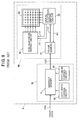
- FIG. 9 is a block diagram showing the structure of a conventional matrix-type display device with a built-in frame memory.
- reference numeral 70 denotes an input control section that controls the timing etc. of input image data
- reference numeral 80 denotes a display-panel module that displays the input image data.
- the input control section 70 has a graphics memory 11 that can temporarily store input image data at least in frame units, a data-write control circuit 12 comprising a microprocessor or the like with an address bus, a data bus, control signal lines, and the like, that carries out control when the input image data are written in the graphics memory 11, and a data-read control circuit 13 that reads the image data temporarily stored in the graphics memory 11 and transfers the data to the display-panel module 80.
- a graphics memory 11 that can temporarily store input image data at least in frame units
- a data-write control circuit 12 comprising a microprocessor or the like with an address bus, a data bus, control signal lines, and the like, that carries out control when the input image data are written in the graphics memory 11, and a data-read control circuit 13 that reads the image data temporarily stored in the graphics memory 11 and transfers the data to the display-panel module 80.
- the display-panel module 80 has: a frame memory 21 that can store image data transferred from the input control section 70 in at least frame units; a display panel 22 in which picture-element units are provided at intersections in a matrix formed by a plurality of signal lines laid out in parallel columns and a plurality of signal lines laid out in parallel rows; a signal-electrode driving circuit 23 that generates a clock signal as a reference for displaying an image on the display panel 22 and, based on the clock signal, generates control signals for reading image data from the frame memory 21 and driving the signal lines of the display panel 22, and generates a frame synchronization signal and a line synchronization signal of the display panel 22; and a scan-electrode driving circuit 24 that generates control signals based on the frame synchronization signal and line synchronization signal to drive the scanning lines of the display panel 22.
- the display panel 22 is, for example, a liquid-crystal display panel with liquid-crystal display elements disposed in a matrix array.
- the image data input to the matrix-type display device 9 from the outside and written in the graphics memory 11 are GD1; the image data read from the graphics memory 11 and transferred to the frame memory 21 are GD2; the image data read from the frame memory 21 and input to the signal-electrode driving circuit 23 are GD3.
- the frame synchronization signal output from the signal-electrode driving circuit 23 to the scan-electrode driving circuit 24 is FS; the line synchronization similarly output from the signal-electrode driving circuit 23 to the scan-electrode driving circuit 24 is LS; the read control signal likewise output from the signal-electrode driving circuit 23 to read the stored contents of the frame memory 21 is RC.
- the operation of the matrix-type display device 9 will be described with reference to the image-data transfer timing diagram in FIG. 10, as well as to FIG. 9.
- Image data GD1 are input to the input control section 70 of the matrix-type display device 9 from the outside by a communication function or the like and stored temporarily in the graphics memory 11 under control of the data-write control circuit 12.
- those image data are immediately read out by the data-read control circuit 13 and transferred to the frame memory 21 as image data GD2, as shown in FIG. 10.
- the image data stored in the frame memory 21 are read out periodically by the signal-electrode driving circuit 23 as image data GD3, in a refresh cycle based on an independently generated clock signal, as shown in FIG. 10, and are input to the signal-electrode driving circuit 23.
- the signal-electrode driving circuit 23 uses the independent clock to generate the read control signal RC and sends it to the frame memory 21, generates and outputs control signals for the signal electrodes of the matrix display panel 22, and generates a frame synchronization signal FS and line synchronization signal LS and sends them to the scan-electrode driving circuit 24.
- the scan-electrode driving circuit 24 generates and outputs control signals for the scanning electrodes of the matrix display panel 22, based on the frame synchronization signal FS and line synchronization signal LS.
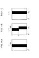
- FIGs. 11A to 11C are drawings showing a thick vertical line moving from the left edge toward the right edge on the matrix display panel 22 of the matrix-type display device 9.
- the frame frequency of the display panel 22 is generally about sixty frames per second, several times the frequency of data transfer from the graphics memory 11 to the frame memory 21.
- the transfer of image data GD2 is carried out asynchronously with respect to the readout of image data GD3 from the frame memory 21 to the matrix display panel 22. If the image data GD3 read from the frame memory 21 for each frame are, in proceeding temporal order, the n-th frame, the (n + 1)-th frame, and the (n + 2)-th frame, as shown in FIG. 10, then the image of the n-th frame, with the vertical line 100a, is first displayed continuously as in FIG. 11A.
- An object of the present invention is to improve the display of moving images in mobile information-terminal equipment.
- the invented matrix-type display device has a matrix display panel and a frame memory.
- a signal-electrode driving circuit generates a frame synchronization signal and a line synchronization signal, and generates control signals for reading the image data from the frame memory and driving the signal lines of the matrix display panel. From the frame synchronization signal and line synchronization signal, a scan-electrode driving circuit generates control signals that drive the scanning electrodes of the matrix display panel. Frames of image data read from the frame memory are thereby displayed on the matrix display panel.
- the invented matrix-type display device also has a graphics memory for temporary buffering of input image data, a data-write control circuit that controls the writing of image data into the graphics memory, and a data-read control circuit that transfers the image data from the graphics memory to the frame memory.
- the data-write control circuit outputs a write-end signal at the completion of the writing of a frame of image data into the graphics memory.
- the invented matrix-type display device further includes a synchronizing circuit that generates a read-start signal from the first frame synchronization signal occurring after a write-end signal.
- the read-start signal causes the read-control circuit to start transferring image data from the graphics memory to the frame memory.
- the writing of image data into the frame memory is thereby synchronized with the reading of image data out of the frame memory.
- the synchronization is arranged so that the write address never overtakes the read address during the reading of a frame of image data.
- the invented matrix-type display device may also have a delay circuit that delays the frame synchronization signal before input to the synchronizing circuit.
- the delay can be set to provide optimal read-write synchronization for the frame memory, for various different types of matrix display panels.
- the delay circuit preferably also receives the line synchronization signal, and delays the frame synchronization signal by a predetermined number of line synchronization pulses. Optimal read-write synchronization of the frame memory can then be maintained despite clock-signal frequency variations.
- the matrix display panel may be, for example, a liquid-crystal display panel of the reflective type, the reflective semi-transmissive type, the active-matrix type, or the fast-response super-twisted birefringent type.
- the matrix display panel may be an organic electroluminescent panel or an active-matrix organic electroluminescent panel.
- Matrix-type display devices according to the present invention will be described specifically below on the basis of drawings showing embodiments thereof.
- those parts having the same functions as in the conventional matrix-type display device 9 described above using FIGs. 9 to 11 are shown with the same reference characters, and redundant descriptions will be omitted.
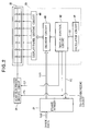
- FIG. 1 is a drawing showing a first matrix-type display device embodying the present invention.
- the principal way in which the matrix-type display device 1 of FIG. 1 differs from the matrix-type display device 9 of FIG. 9 is that, in the input control unit 10, there is a synchronizing circuit 14 that outputs a read-start signal to the data-read control circuit 13 in synchronization with the frame synchronization signal FS output from the signal-electrode driving circuit 23 in the display-panel module 20.
- the data-write control circuit 12 is adapted to be able to output a write-end signal WE to the synchronizing circuit 14
- the signal-electrode driving circuit 23 is adapted to be able to send the frame synchronization signal both to the scan-electrode driving circuit 24 and the synchronizing circuit 14.
- the rest of the structure it is the same as in the conventional matrix-type display device 9 shown in FIG. 11, so a description will be omitted.
- FIG. 2 is a block diagram showing the internal structure of the signal-electrode driving circuit 23 in the display-panel module 20 in FIG. 1.
- reference numeral 41 denotes an oscillator circuit that generates a clock signal (reference signal) SS, which becomes a reference for displaying images on the matrix display panel 22.
- Reference numeral 42 denotes a display control circuit that outputs the read control signal RC to the frame memory 21, outputs the frame synchronization signal FS and line synchronization signal LS to the scan-electrode driving circuit 24, and outputs a synchronization signal for decoding the image data to a decoder circuit 43, described below, based on the reference signal SS.
- the frame synchronization signal FS is also output from the display control circuit 42 to the synchronizing circuit 14.
- Reference numeral 43 denotes the decoder circuit, which converts (decodes) the coded image data GD3 to image-displayable image data, based on image data coding rules and the synchronization signal from the display control circuit 42.
- Reference numeral 44 denotes a display-panel driving circuit that drives the signal electrodes of the matrix display panel 22 by applying voltages thereto, on the basis of the decoded image data.
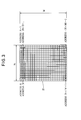
- FIG. 3 is a drawing showing the address structure of the frame memory 21 in FIG. 1.
- the data-read control circuit 13 writes one screen of image data read from the graphics memory 11 in sequence from address 0 to address N ⁇ M - 1 in the frame memory 21, which is an N ⁇ M frame memory, as shown in FIG. 3, N being the horizontal dot count and M the vertical line count in the matrix-type display device 1.
- the data-read control circuit 13 writes the image data in the first line from address 0 to address N - 1, then writes the image data in the second line from address N to address N ⁇ 2 - 1. Writing each line of image data in similar fashion, it completes the writing of one screen by writing the M-th line, which is the last line, from address N ⁇ (M - 1) to address N ⁇ M - 1.
- the data read out after being temporarily written in the frame memory 21 are not limited to image data, but may be, for example, data constituting characters or the like. Furthermore, in a mobile telephone supporting moving images according to the IMT-2000 standard, due to restrictions on data communication speed and the like, for the present, transfer speeds up to about fifteen screens per second are envisioned as the data transfer speed of the frame memory 21. It is expected, however, that this transfer speed will increase to about thirty screens per second in the future.
- the image data GD1 input to the input control unit 10 of the matrix-type display device 1 from the outside through a communication function or the like are temporarily stored in the graphics memory 11 under control of the data-write control circuit 12.
- the write-end signal WE is output from the data-write control circuit 12 to the synchronizing circuit 14.
- the synchronizing circuit 14 is reset by the input of this write-end signal WE, and then carries out the operations below.
- the synchronizing circuit 14 After receiving the write-end signal WE, the synchronizing circuit 14 waits for the next frame synchronization signal FS to be input, and outputs a read-start signal RK to the data-read control circuit 13 in synchronization of the input thereof, at timing t3 in FIG. 4. Thereupon, the image data GD1 temporarily stored in the graphics memory 11 are read, starting at timing t3, and transferred as image data GD2 to the frame memory 21 by the data-read control circuit 13.
- the image data stored in the frame memory 21 are read out periodically as image data GD3 by the signal-electrode driving circuit 23, in a refresh cycle based on the reference signal (clock signal) SS generated by the oscillator circuit 41, and input to the signal-electrode driving circuit 23.
- the frames of image data GD3 read from the frame memory 21 are numbered n, (n + 1), (n + 2), and so on, the frame number increasing in temporal order.
- n is a non-negative integer.
- the display control circuit 42 In the signal-electrode driving circuit 23, the display control circuit 42 generates the read control signal RC and outputs it to the frame memory 21, outputs a decoding synchronization signal to the decoder circuit 43, and generates the frame synchronization signal FS and line synchronization signal LS and outputs them to the scan-electrode driving circuit 24, based on the reference signal SS.
- the decoder circuit 43 decodes the input image data GD3 to image data that are image-displayable on the matrix display panel 22, based on the synchronization signal from the display control circuit 42 and the image data decoding rules.
- the display-panel driving circuit 44 generates control signals from the decoded image data and outputs them to the signal electrodes of the matrix display panel 22.
- the scan-electrode driving circuit 24 generates control signals for the scan electrodes of the matrix display panel 22 and outputs them, based on the frame synchronization signal FS and line synchronization signal LS.
- the transfer of image data GD2 from the graphics memory 11 to the frame memory 21 starts (at timing t3) before the reading of the image data GD3 for frame (n + 2) from the frame memory 21 starts (at timing t4), and ends before the reading of the image data GD3 for frame (n + 2) ends. Accordingly, it is always the newly transferred and stored image data GD2 that are read as the image data GD3 for frame (n + 2); no switchover from old to new image data occurs during the reading of frame (n + 2) from the frame memory 21.
- the transfer of the image data GD2 from the graphics memory 11 to the frame memory 21 also starts after the reading of the image data GD3 for frame (n + 1) starts, and ends after the reading of the image data GD3 for frame (n + 1) ends. Accordingly, it is always the previously transferred and stored image data that are read as the image data GD3 for frame (n + 1); no switchover from old to new image data occurs during the reading of frame (n + 1).
- FIGs. 5A to 5C are drawings showing a thick vertical line moving from the left edge toward the right edge on the matrix display panel 22 of the matrix-type display device 1. These drawings illustrate frames n, (n + 1), and (n + 2) in FIG. 4.
- the same image data GD3 are read again from the frame memory 21 and an identical vertical line 100b is displayed in frame (n + 1), as in FIG. 5B.
- the data-read control circuit 13 begins writing new image data GD2 into the frame memory 21, but the GD2 write address lags the GD3 read address, so the newly written image data GD2 are not read yet.
- the writing of new image data GD2 into the frame memory 21 continues during the next frame (n + 2).
- the GD3 read address now lags the GD2 write address, so a completely new image is displayed, with a new continuous vertical line 101b shifted to the right as in FIG. 5C.
- the process of transferring the image data GD2 into the frame memory 21 and the process of reading the image data GD3 from the frame memory 21 to the signal-electrode driving circuit 23 do not match up at the same address, and the data transfer is controlled so that during one frame of the image displayed on the matrix display panel 22, there is no switchover to the next frame, so when a moving image is displayed, situations in which the image content of the upper part and lower part of one screen are temporally out of step do not occur, and a smooth picture can be displayed.
- the first embodiment avoided the switching of the image to a newly written image midway through the image data GD3 read from the frame memory 21 by synchronizing the timing of the start of the transfer of image data GD2 from the graphics memory 11 to the frame memory 21 with the frame synchronization signal FS, with a delay time DT1 from the frame synchronization signal FS to the reading of the image data GD3 from the frame memory 21. If the delay time DT1 is increased, however, then the timing of the end of the transfer of image data GD2 approaches the timing of the end of the reading of the image data GD3 of frame (n + 1) in FIG.
- the second embodiment adjusts the delay time from the transfer of image data GE2 to the reading of image data GD3 so that it does not become too long.
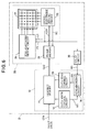
- FIG. 6 is a block diagram showing the structure of the matrix-type display device of the second embodiment of the present invention.
- a delay circuit 30 is provided to delay the frame synchronization signal FS output from the signal-electrode driving circuit 23 by a predetermined time to synchronize it with the timing of the end of the reading of the image data GD3 of an arbitrary frame, and output it as a read synchronization signal RS.
- a delay circuit 30 is provided to delay the frame synchronization signal FS output from the signal-electrode driving circuit 23 by a predetermined time to synchronize it with the timing of the end of the reading of the image data GD3 of an arbitrary frame, and output it as a read synchronization signal RS.
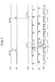
- the GD1, WE, FS, and GD3 waveforms in FIG. 7 are identical to the corresponding waveforms in FIG. 4.
- the waveform of the read synchronization signal RS is delayed from the frame synchronization signal FS by a predetermined amount DT2 by the delay circuit 30, so as to be synchronized with the timing t5 of the end of the reading of the image data GD3 of frame (n + 1).
- the transfer of the image data GD2 starts in synchronization with the read synchronization signal RS at timing t5.
- the frame synchronization signal FS is not input directly to the synchronizing circuit 14, but the read synchronization signal RS delayed in the delay circuit 30 is input to the synchronizing circuit 14, producing a delay time DT3 obtained by shortening delay time DT1 by the delay time DT2 of the delay circuit 30.
- the read synchronization signal RS is generated in synchronization with the timing t5 of the end of the reading of the image data GD3 of the (n + 1)-th frame, so a situation in which, midway through one frame of the image displayed on the matrix display panel 22, there is a switchover to the image of the next frame can be eliminated.
- the second embodiment can set an optimal delay quantity in the delay circuit 30 for matrix display panels having different response speeds, such as a TFT or other active-matrix liquid-crystal display panel with a response speed of about 30-50 msec, a fast-response STN liquid-crystal panel with a response speed of about 70-80 msec, or an organic EL panel with a response speed of a few microseconds;
- the delay time of the output read synchronization signal RS can be set so that it is not too long, regardless of the type of matrix display panel; the second embodiment can accordingly display smooth moving images even if the frame synchronization signal FS from the signal-electrode driving circuit 23 is inappropriate as the transfer timing of image data GD2.
- the second embodiment eliminated the situation in which, midway through one frame of the image displayed on the matrix display panel 22, there is a switchover to the image of the next frame by adding a delay circuit 30 to which the frame synchronization signal FS is input, and which outputs that signal FS as a read synchronization signal RS optimally delayed so as to synchronize with the timing t5 of the end of the reading of the image data GD3, as a pre-stage of the frame synchronization signal input section of the synchronizing circuit 14, but the clock signal used in the delay circuit 30 is not necessarily the same as the clock signal (reference signal SS) of the signal-electrode driving circuit 23.
- reference signal SS differs from the clock signal used in the delay circuit 30, then due to variations in their oscillator circuits, it may happen that the read synchronization signal RS cannot be set to the optimal delay quantity.
- the third embodiment synchronizes the read synchronization signal RS to the internal clock signal (reference signal SS) of the signal-electrode driving circuit 23, so that it is not easily affected by oscillator-circuit variations.
- FIG. 8 is a block diagram showing the structure of the matrix-type display device of the third embodiment of the present invention.
- the third embodiment is adapted to use the line synchronization signal LS as the clock signal of the delay circuit 31. As for the rest of the structure, it is the same as in the matrix-type display device 2 of the second embodiment, shown in FIG. 6, so a description will be omitted.
- the read synchronization signal RS in FIG. 7 fails to match the timing t5 of the end of the reading of the image data GD3 of frame (n + 1), for example. Then the transfer of image data GD2 synchronized with the read synchronization signal RS also fails to match the timing t5 of the end of the reading of image data GD3, and the possibility of the occurrence of a switchover, midway through one frame of the image displayed on the matrix display panel 22, to the image of the next frame arises once again.
- the frame synchronization signal FS and line synchronization signal LS output from the signal-electrode driving circuit 23 are generated on the basis of the same reference signal SS from the oscillator circuit 41, so even if variations between oscillator circuits occur, the synchronization between the frame synchronization signal FS and line synchronization signal LS does not vary.
- the third embodiment is therefore structured to input the line synchronization signal LS as the clock signal of the delay circuit 31, as shown in FIG. 8.
- a signal obtained by delaying the frame synchronization signal FS by a preset number of pulses of the line synchronization signal LS can then be output from the delay circuit 31 as the read synchronization signal RS.
- the amount by which the read synchronization signal RS is delayed from the frame synchronization signal FS does not vary, so the transfer of image data GD2 in synchronization with the read synchronization signal RS can be synchronized reliably with the timing t5 of the end of the reading of the image data GD3 of frame (n + 1). Accordingly, the situation in which, midway through one frame of the image displayed on the matrix display panel 22, there is a switchover to the image of the next frame can be eliminated.
- the third embodiment thus inputs the line synchronization signal LS, as well as the frame synchronization signal FS, to the delay circuit 31, and outputs the read synchronization signal RS by delaying the frame synchronization signal FS with the line synchronization signal LS as a clock, so the timing of the generation of the read synchronization signal RS does not vary due to variations in oscillator circuits or the like, a read synchronization signal RS having an optimal delay can be output, and a read synchronization signal RS of the optimal delay, delayed by a fixed phase quantity from the frame synchronization signal FS, can be set, so a smooth, stable moving image can be displayed regardless of the type of matrix display panel, whether it is an active-matrix liquid-crystal panel, a fast-response STN liquid-crystal panel, an organic EL panel, or the like, for example, without being affected by oscillator-circuit variations, even in conditions in which oscillator-circuit frequency drift etc. is likely to occur.
- the matrix display panel in the embodiments above is a liquid-crystal panel, it can be classified as being of the transmissive type, the reflective type, or the reflective semi-transmissive type.
- the transmissive type of liquid-crystal panel requires internal illumination such as back-lighting to make the content of the image display visible, and back-lighting requires electrical power, so it is difficult to use in mobile information-terminal equipment, such as a mobile telephone or the like, for which low power consumption is desired.
- the reflective type does not require electric power for back-lighting, because the content of the displayed image is made visible by external light reflected from a reflecting plate provided on the whole of the back surface, making it suitable for mobile information-terminal equipment, such as a mobile telephone or the like, for which low power consumption is desired.
- the reflective semi-transmissive type provides a semi-transmissive reflecting plate such as a mesh-type panel on the back surface, so that the content of the image display can be made visible by the reflection of external light and by internal illumination; normally, as in the reflective type, the electric power for back-lighting is unnecessary, but in addition, when the exterior surroundings are dark the display can be viewed by the use of internal illumination, so it is suitable for mobile information-terminal equipment, such as a mobile telephone or the like, for which low power consumption is desired, and is more convenient because visibility in dark places is improved.
- liquid-crystal display panel of the active-matrix type is used as the matrix display panel, compared with the conventional liquid-crystal display panel of the STN type with a slow response speed, the response speed and the contrast of the display section with respect to the surroundings are improved, so even when moving images with vigorous motion or moving images that move rapidly are displayed, a smooth, stable moving image can be displayed, and its visibility can be improved.
- a fast-response STN liquid-crystal display panel is used as the matrix display panel, compared with the conventional liquid-crystal display panel of the STN type with a slow response speed, the response speed is improved, so even when moving images with vigorous motion or moving images that move rapidly are displayed, a smooth, stable moving image can be displayed, while lower power consumption and low cost are maintained.
- an organic electroluminescent display panel is used as the matrix display panel, compared with the conventional liquid-crystal display panel of the STN type with a slow response speed, the response speed is improved as with a liquid-crystal display panel of the active-matrix type.
- the contrast of the display section with respect to its surroundings is improved through the emission of light by the display section itself, so not only can a smooth, stable moving image be displayed, but in addition, visibility can be improved even more than with a liquid crystal, so the image quality can be further improved, and the display can be slimmed because back-lighting is not required.
- an organic electroluminescent display panel of the active-matrix type is used as the matrix display panel, then a smooth, stable moving image can be displayed, even when moving images with vigorous motion or moving images that move rapidly are displayed, and visibility can be improved even more than with a liquid crystal, so the image quality can be further improved, and the display can be slimmed.
- the process of transferring the image data into the frame memory and the process of reading the image data from the frame memory to the signal-electrode driving circuit do not match up at the same address, and the data transfer is controlled so that during one frame of the image displayed on the matrix display panel, it does not switch to the next frame, so when a moving image is displayed, situations in which the image content of the upper part and lower part of one screen are temporally out of step do not occur, and a smooth picture can be displayed.
- a delay circuit that outputs a read synchronization signal, obtained by delaying the frame synchronization signal, as a pre-stage of the frame synchronization signal input section of the synchronizing circuit, it becomes possible to set an appropriate delay quantity in the delay circuit, not making the delay time too long, for matrix display panels having different response speeds, and output it as a read synchronization signal, so in addition to the above effects, regardless of the type of matrix display panel, it can display a smooth moving image even if the frame synchronization signal from the signal-electrode driving circuit is inappropriate as the transfer timing of image data.
- the line synchronization signal, as well as the frame synchronization signal is input to the delay circuit, and the read synchronization signal is output by delaying the frame synchronization signal with the line synchronization signal as a clock, so the timing of the generation of the read synchronization signal does not vary due to variations in oscillator circuits or the like, a read synchronization signal having the optimal delay can be output, and a read synchronization signal of the optimal delay, delayed by a fixed phase quantity from the frame synchronization signal, can be set, so in addition to the effects described above, a smooth, stable moving image can be displayed regardless of the type of matrix display panel, without being affected by oscillator-circuit variations, even in conditions in which oscillator-circuit frequency drift etc. is likely to occur.
- a liquid-crystal display panel is used as the display panel of the matrix-type display device, so in addition to the effects described above, a matrix-type display device satisfying the conditions of reduced power consumption and reduced thickness and weight, thus optimal for use in mobile information terminals such as mobile telephones and the like, can be provided.
- a reflective liquid-crystal panel not requiring internal illumination, is used as the display panel of the matrix-type display device, so in addition to the effects described above, a matrix-type display device with even lower power consumption can be provided.
- a reflective semi-transmissive liquid-crystal display panel not requiring internal illumination when external light can be used, but able to employ internal illumination when the exterior surroundings are dark, is used as the display panel of the matrix-type display device, so in addition to the effects described above, a convenient matrix-type display device can be provided.
- an active-matrix liquid-crystal display panel with a fast response speed is used as the display panel of the matrix-type display device, so a matrix-type display device can be provided that displays an image with good image quality and little motion blur, even when moving images with vigorous motion or moving images that move rapidly are displayed.
- a fast-response STN liquid-crystal display panel is used as the display panel of the matrix-type display device, so a matrix-type display device can be provided that is low in cost and power consumption, and displays an image with little motion blur, even when moving images with vigorous motion or moving images that move rapidly are displayed.
- an organic EL display panel is used as the display panel of the display panel of the matrix-type display device, so a matrix-type display device can be provided that is low in power consumption and has a thin structure, and displays an image with extremely good image quality, with almost no motion blur.
- an active-matrix organic EL display panel is used as the display panel of the matrix-type display device, so a matrix-type display device can be provided that is low in power consumption and has a thin structure, and displays an image with extremely good image quality, with almost no motion blur, even when moving images with vigorous motion or moving images that move rapidly are displayed.
- a liquid-crystal panel of the active-matrix type may have thin-film transistors or thin-film diodes.
- An organic EL panel of the active-matrix type may have thin-film transistors.
Landscapes
- Engineering & Computer Science (AREA)
- Physics & Mathematics (AREA)
- Computer Hardware Design (AREA)
- General Physics & Mathematics (AREA)
- Theoretical Computer Science (AREA)
- Control Of Indicators Other Than Cathode Ray Tubes (AREA)
- Control Of El Displays (AREA)
- Liquid Crystal Display Device Control (AREA)
- Controls And Circuits For Display Device (AREA)
- Transforming Electric Information Into Light Information (AREA)
Abstract
Description
Claims (11)
- A matrix-type display device (1) including:wherein said data-write control circuit (12) outputs a write-end signal at the completion of the writing of one frame of image data in the graphics memory (11);a display panel (22) provided with picture-element units at intersections in a matrix formed by a plurality of signal lines laid out in parallel columns and a plurality of scanning lines laid out in parallel rows;a frame memory (21) for storing image data to be displayed on the display panel (22) a frame at a time;a signal-electrode driving circuit (23) for generating a frame synchronization signal and a line synchronization signal, and generating control signals for reading the image data from said frame memory (21) and driving the signal lines of said display panel (22);a scan-electrode driving circuit (24) for generating control signals to drive the scanning lines of said display panel (22), according to said frame synchronization signal and said line synchronization signal;a graphics memory (11) for temporarily storing input image data a frame at a time;a data-write control circuit (12) for controlling writing of said input image data in the graphics memory (11); anda data-read control circuit (13) for transferring the image data written in said graphics memory (11) to the frame memory (21) ;
further including a synchronizing circuit (14) for generating a read-start signal from said frame synchronization signal following said write-end signal, the read-start signal causing the data-read control circuit (13) to start transferring the image data from the graphics memory (11) to the frame memory (21). - The matrix-type display device (2) of claim 1, further including a delay circuit (30) for delaying said frame synchronization signal by a predetermined amount and supplying the delayed frame synchronization signal to said synchronizing circuit (14), thereby adjusting the timing of the read-start signal so that the transfer of data from said graphics memory (11) to said frame memory (21) ends after said signal-electrode driving circuit (23) has read one frame of image data from said frame memory (21), and before said signal-electrode driving circuit (23) has finished reading the next frame of image data.
- The matrix-type display device (3) of claim 2, wherein said delay circuit (31) uses said line synchronization signal as a clock signal, and delays said frame synchronization signal by a predetermined number of pulses of said line synchronization signal.
- The matrix-type display device of claim 1, wherein said display panel (22) is a liquid-crystal display panel.
- The matrix-type display device of claim 4, wherein said liquid-crystal display panel is of a reflective type, enabling the display content to be seen by reflection of externally incident light.
- The matrix-type display device of claim 4, wherein said liquid-crystal display panel is of a reflective semi-transmissive type, enabling display content to be seen by reflection of externally incident light and by transmitted light.
- The matrix-type display device of claim 4, wherein said liquid-crystal display panel is of an active-matrix type.
- The matrix-type display device of claim 4, wherein said liquid-crystal display panel is of a fast-response super-twisted birefringent type.
- The matrix-type display device of claim 1, wherein said display panel (22) is an organic electroluminescent panel.
- The matrix-type display device of claim 9, wherein said organic electroluminescent panel is of an active-matrix type.
- A circuit for use with a matrix-type display device comprising a first frame memory (21) for storing frame data to be displayed on the display, a second memory (11) for storing frame data, and control means (10) for controlling the transfer of data from the second memory (11) to the first memory (21) in accordance with the frame cycle of the display.
Applications Claiming Priority (2)
| Application Number | Priority Date | Filing Date | Title |
|---|---|---|---|
| JP2000293760 | 2000-09-27 | ||
| JP2000293760A JP3611511B2 (en) | 2000-09-27 | 2000-09-27 | Matrix type display device, image data display method, and portable information terminal device |
Publications (3)
| Publication Number | Publication Date |
|---|---|
| EP1193671A2 true EP1193671A2 (en) | 2002-04-03 |
| EP1193671A3 EP1193671A3 (en) | 2003-04-23 |
| EP1193671B1 EP1193671B1 (en) | 2004-09-08 |
Family
ID=18776494
Family Applications (1)
| Application Number | Title | Priority Date | Filing Date |
|---|---|---|---|
| EP01308110A Expired - Lifetime EP1193671B1 (en) | 2000-09-27 | 2001-09-24 | Matrix-type display device |
Country Status (5)
| Country | Link |
|---|---|
| US (1) | US6700571B2 (en) |
| EP (1) | EP1193671B1 (en) |
| JP (1) | JP3611511B2 (en) |
| CN (1) | CN1157703C (en) |
| DE (1) | DE60105365T2 (en) |
Cited By (3)
| Publication number | Priority date | Publication date | Assignee | Title |
|---|---|---|---|---|
| WO2005073955A1 (en) * | 2004-01-28 | 2005-08-11 | Koninklijke Philips Electronics N.V. | Displaying on a matrix display |
| EP1600917A4 (en) * | 2003-02-25 | 2007-11-07 | Mitsubishi Electric Corp | MATRIX TYPE SCREEN AND METHOD OF USE |
| EP1665775B1 (en) * | 2003-09-22 | 2012-10-24 | Samsung Electronics Co., Ltd. | Display synchronization signal generation apparatus in digital broadcast receiver and decoder |
Families Citing this family (22)
| Publication number | Priority date | Publication date | Assignee | Title |
|---|---|---|---|---|
| FI115802B (en) * | 2000-12-04 | 2005-07-15 | Nokia Corp | Updating picture frames in a screen with memory |
| US7009604B2 (en) * | 2002-07-19 | 2006-03-07 | Sun Microsystems, Inc. | Frame detector for use in graphics systems |
| KR100490420B1 (en) * | 2002-12-26 | 2005-05-17 | 삼성전자주식회사 | Apparatus and method for generating programmable drive signal in display panel |
| JP2004226522A (en) * | 2003-01-21 | 2004-08-12 | Hitachi Displays Ltd | Display device and driving method thereof |
| JP4393106B2 (en) * | 2003-05-14 | 2010-01-06 | シャープ株式会社 | Display drive device, display device, and portable electronic device |
| JP2006030389A (en) * | 2004-07-13 | 2006-02-02 | Alpine Electronics Inc | Information processor, system, display method, and program |
| KR100582402B1 (en) * | 2004-09-10 | 2006-05-22 | 매그나칩 반도체 유한회사 | Memory read / write timing control method supporting flicker-free display in panel and TDC panel driving device using the method |
| JP2006174363A (en) * | 2004-12-20 | 2006-06-29 | Nec Electronics Corp | Frame synchronizer, optical disk drive, information recording/reproducing device, and signal synchronizing method |
| DE102006003531A1 (en) * | 2006-01-24 | 2007-08-02 | Schott Ag | Transporting, homogenizing and/or conditioning glass melt comprises adjusting residence time of melt in transporting and/or conditioning device using section of wall of device |
| JP2007248965A (en) * | 2006-03-17 | 2007-09-27 | Yazaki Corp | Graphic display device and graphic display method |
| KR100805610B1 (en) * | 2006-08-30 | 2008-02-20 | 삼성에스디아이 주식회사 | Organic electroluminescent display and its driving method |
| JP2008216362A (en) * | 2007-02-28 | 2008-09-18 | Optrex Corp | Driving device for display apparatus |
| JP5242076B2 (en) * | 2007-04-13 | 2013-07-24 | グローバル・オーエルイーディー・テクノロジー・リミテッド・ライアビリティ・カンパニー | Active matrix display device |
| JP5407137B2 (en) * | 2007-11-22 | 2014-02-05 | 日亜化学工業株式会社 | Lighting device, lighting unit |
| JP5399163B2 (en) | 2009-08-07 | 2014-01-29 | グローバル・オーエルイーディー・テクノロジー・リミテッド・ライアビリティ・カンパニー | Display device |
| JP5508836B2 (en) | 2009-12-24 | 2014-06-04 | 株式会社メガチップス | Setting control apparatus and operation method of setting control apparatus |
| JP5606746B2 (en) * | 2010-01-27 | 2014-10-15 | 京セラ株式会社 | Mobile terminal device |
| KR101861723B1 (en) | 2011-12-20 | 2018-05-30 | 삼성전자주식회사 | Devices and method of adjusting synchronization signal preventing tearing and flicker |
| JP2014052548A (en) * | 2012-09-07 | 2014-03-20 | Sharp Corp | Memory controller, portable terminal, memory control program and computer readable recording medium |
| KR102456654B1 (en) | 2014-11-26 | 2022-10-18 | 가부시키가이샤 한도오따이 에네루기 켄큐쇼 | Display device and electronic device |
| CN114281295B (en) * | 2020-09-18 | 2024-03-15 | 西安诺瓦星云科技股份有限公司 | Image processing method and device and LED display screen system |
| CN115457917B (en) * | 2022-09-28 | 2025-09-26 | 昆山龙腾光电股份有限公司 | Display device and signal transmission method thereof |
Family Cites Families (11)
| Publication number | Priority date | Publication date | Assignee | Title |
|---|---|---|---|---|
| US5095301A (en) * | 1985-11-06 | 1992-03-10 | Texas Instruments Incorporated | Graphics processing apparatus having color expand operation for drawing color graphics from monochrome data |
| DE69215155T2 (en) * | 1991-07-26 | 1997-06-19 | Sun Microsystems Inc | Device with fast copying between raster buffers in a display system with double buffer memories |
| DE4231158C5 (en) * | 1991-09-17 | 2006-09-28 | Hitachi, Ltd. | Method and device for the composition and display of images |
| JP3582082B2 (en) | 1992-07-07 | 2004-10-27 | セイコーエプソン株式会社 | Matrix display device, matrix display control device, and matrix display drive device |
| JPH06282643A (en) * | 1993-03-29 | 1994-10-07 | Matsushita Electric Ind Co Ltd | Picture synthesizing effect device |
| US5446496A (en) * | 1994-03-31 | 1995-08-29 | Hewlett-Packard Company | Frame rate conversion with asynchronous pixel clocks |
| AU3548095A (en) * | 1994-08-31 | 1996-03-22 | S3 Incorporated | Apparatus for correction of video tearing |
| JP3307807B2 (en) * | 1995-09-29 | 2002-07-24 | 三洋電機株式会社 | Video signal processing device |
| JPH1195728A (en) | 1997-09-25 | 1999-04-09 | Hitachi Ltd | Liquid crystal display controller |
| JP3811251B2 (en) | 1997-04-24 | 2006-08-16 | 旭硝子株式会社 | Driving device for liquid crystal display device |
| KR100613438B1 (en) * | 1999-11-17 | 2006-08-18 | 엘지.필립스 엘시디 주식회사 | Reflective type liquid crystal display device and manufacturing method thereof |
-
2000
- 2000-09-27 JP JP2000293760A patent/JP3611511B2/en not_active Expired - Fee Related
-
2001
- 2001-09-24 EP EP01308110A patent/EP1193671B1/en not_active Expired - Lifetime
- 2001-09-24 DE DE60105365T patent/DE60105365T2/en not_active Expired - Lifetime
- 2001-09-26 US US09/962,166 patent/US6700571B2/en not_active Expired - Lifetime
- 2001-09-27 CN CNB011411015A patent/CN1157703C/en not_active Expired - Fee Related
Cited By (4)
| Publication number | Priority date | Publication date | Assignee | Title |
|---|---|---|---|---|
| EP1600917A4 (en) * | 2003-02-25 | 2007-11-07 | Mitsubishi Electric Corp | MATRIX TYPE SCREEN AND METHOD OF USE |
| EP1665775B1 (en) * | 2003-09-22 | 2012-10-24 | Samsung Electronics Co., Ltd. | Display synchronization signal generation apparatus in digital broadcast receiver and decoder |
| WO2005073955A1 (en) * | 2004-01-28 | 2005-08-11 | Koninklijke Philips Electronics N.V. | Displaying on a matrix display |
| US8466924B2 (en) | 2004-01-28 | 2013-06-18 | Entropic Communications, Inc. | Displaying on a matrix display |
Also Published As
| Publication number | Publication date |
|---|---|
| DE60105365T2 (en) | 2005-09-29 |
| EP1193671A3 (en) | 2003-04-23 |
| CN1347069A (en) | 2002-05-01 |
| JP3611511B2 (en) | 2005-01-19 |
| US6700571B2 (en) | 2004-03-02 |
| CN1157703C (en) | 2004-07-14 |
| JP2002108268A (en) | 2002-04-10 |
| US20020041277A1 (en) | 2002-04-11 |
| EP1193671B1 (en) | 2004-09-08 |
| DE60105365D1 (en) | 2004-10-14 |
Similar Documents
| Publication | Publication Date | Title |
|---|---|---|
| US6700571B2 (en) | Matrix-type display device | |
| US7567092B2 (en) | Liquid crystal display driver including test pattern generating circuit | |
| US6795066B2 (en) | Display apparatus and driving method of same | |
| KR100445285B1 (en) | Display device | |
| KR100454993B1 (en) | Driver with built-in RAM, display unit with the driver, and electronic device | |
| JP4123711B2 (en) | Electro-optical panel driving method, electro-optical device, and electronic apparatus | |
| JP3578141B2 (en) | Display driver, display unit and electronic device | |
| EP1280127A2 (en) | Active matrix display device | |
| JP2002091396A (en) | Display device and its control method | |
| JP2001343928A (en) | Display device driving circuit, display device driving method, and image display device | |
| JP2009009018A (en) | Source driver, electro-optical device, projection display device, and electronic device | |
| JP2005326859A (en) | Dual panel drive system and drive method | |
| US7969427B2 (en) | Control device for display panel and display apparatus having same | |
| JPH11259053A (en) | Liquid crystal display | |
| JP2008185993A (en) | Electro-optical device, processing circuit, processing method, and projector | |
| US20030146911A1 (en) | Method for generating control signal, control-signal generation circuit, data-line driving circuit, element substrate, optoelectronic device, and electronic apparatus | |
| JP2001159883A (en) | Electro-optical device driving method, driving circuit, electro-optical device, and electronic apparatus | |
| JP3056631B2 (en) | Liquid crystal display | |
| CN112785980B (en) | Display driving device and method and OLED display device | |
| JP2003044008A (en) | Active matrix type display device and control device therefor | |
| JP4709371B2 (en) | Liquid crystal display device and method for stopping voltage supply of liquid crystal display device | |
| KR100741904B1 (en) | LCD and its driving method | |
| JP2002311905A (en) | Liquid crystal display device and image display application device using the same | |
| JP4179396B2 (en) | Electro-optical device and electronic apparatus | |
| KR100516065B1 (en) | High resolution liquid crystal display device and method thereof for enlarged display of low resolution image data |
Legal Events
| Date | Code | Title | Description |
|---|---|---|---|
| PUAI | Public reference made under article 153(3) epc to a published international application that has entered the european phase |
Free format text: ORIGINAL CODE: 0009012 |
|
| AK | Designated contracting states |
Kind code of ref document: A2 Designated state(s): AT BE CH CY DE DK ES FI FR GB GR IE IT LI LU MC NL PT SE TR |
|
| AX | Request for extension of the european patent |
Free format text: AL;LT;LV;MK;RO;SI |
|
| PUAL | Search report despatched |
Free format text: ORIGINAL CODE: 0009013 |
|
| AK | Designated contracting states |
Designated state(s): AT BE CH CY DE DK ES FI FR GB GR IE IT LI LU MC NL PT SE TR |
|
| AX | Request for extension of the european patent |
Extension state: AL LT LV MK RO SI |
|
| RIC1 | Information provided on ipc code assigned before grant |
Ipc: 7G 09G 5/18 B Ipc: 7G 09G 3/20 A Ipc: 7G 09G 1/16 B Ipc: 7G 09G 5/393 B |
|
| 17P | Request for examination filed |
Effective date: 20030917 |
|
| AKX | Designation fees paid |
Designated state(s): DE FR GB |
|
| GRAP | Despatch of communication of intention to grant a patent |
Free format text: ORIGINAL CODE: EPIDOSNIGR1 |
|
| GRAS | Grant fee paid |
Free format text: ORIGINAL CODE: EPIDOSNIGR3 |
|
| GRAA | (expected) grant |
Free format text: ORIGINAL CODE: 0009210 |
|
| AK | Designated contracting states |
Kind code of ref document: B1 Designated state(s): DE FR GB |
|
| REG | Reference to a national code |
Ref country code: GB Ref legal event code: FG4D |
|
| REG | Reference to a national code |
Ref country code: IE Ref legal event code: FG4D |
|
| REF | Corresponds to: |
Ref document number: 60105365 Country of ref document: DE Date of ref document: 20041014 Kind code of ref document: P |
|
| REG | Reference to a national code |
Ref country code: IE Ref legal event code: MM4A |
|
| PLBE | No opposition filed within time limit |
Free format text: ORIGINAL CODE: 0009261 |
|
| STAA | Information on the status of an ep patent application or granted ep patent |
Free format text: STATUS: NO OPPOSITION FILED WITHIN TIME LIMIT |
|
| ET | Fr: translation filed | ||
| 26N | No opposition filed |
Effective date: 20050609 |
|
| REG | Reference to a national code |
Ref country code: GB Ref legal event code: 746 Effective date: 20110513 |
|
| REG | Reference to a national code |
Ref country code: DE Ref legal event code: R084 Ref document number: 60105365 Country of ref document: DE Effective date: 20110704 Ref country code: DE Ref legal event code: R084 Ref document number: 60105365 Country of ref document: DE Effective date: 20110506 |
|
| PGFP | Annual fee paid to national office [announced via postgrant information from national office to epo] |
Ref country code: GB Payment date: 20120919 Year of fee payment: 12 |
|
| PGFP | Annual fee paid to national office [announced via postgrant information from national office to epo] |
Ref country code: FR Payment date: 20120926 Year of fee payment: 12 |
|
| GBPC | Gb: european patent ceased through non-payment of renewal fee |
Effective date: 20130924 |
|
| REG | Reference to a national code |
Ref country code: FR Ref legal event code: ST Effective date: 20140530 |
|
| PG25 | Lapsed in a contracting state [announced via postgrant information from national office to epo] |
Ref country code: GB Free format text: LAPSE BECAUSE OF NON-PAYMENT OF DUE FEES Effective date: 20130924 |
|
| PG25 | Lapsed in a contracting state [announced via postgrant information from national office to epo] |
Ref country code: FR Free format text: LAPSE BECAUSE OF NON-PAYMENT OF DUE FEES Effective date: 20130930 |
|
| PGFP | Annual fee paid to national office [announced via postgrant information from national office to epo] |
Ref country code: DE Payment date: 20150916 Year of fee payment: 15 |
|
| REG | Reference to a national code |
Ref country code: DE Ref legal event code: R119 Ref document number: 60105365 Country of ref document: DE |
|
| PG25 | Lapsed in a contracting state [announced via postgrant information from national office to epo] |
Ref country code: DE Free format text: LAPSE BECAUSE OF NON-PAYMENT OF DUE FEES Effective date: 20170401 |