CN1157703C - Array display device - Google Patents
Array display device Download PDFInfo
- Publication number
- CN1157703C CN1157703C CNB011411015A CN01141101A CN1157703C CN 1157703 C CN1157703 C CN 1157703C CN B011411015 A CNB011411015 A CN B011411015A CN 01141101 A CN01141101 A CN 01141101A CN 1157703 C CN1157703 C CN 1157703C
- Authority
- CN
- China
- Prior art keywords
- frame
- signal
- mentioned
- display device
- synchronizing signal
- Prior art date
- Legal status (The legal status is an assumption and is not a legal conclusion. Google has not performed a legal analysis and makes no representation as to the accuracy of the status listed.)
- Expired - Fee Related
Links
Images


Classifications
-
- G—PHYSICS
- G09—EDUCATION; CRYPTOGRAPHY; DISPLAY; ADVERTISING; SEALS
- G09G—ARRANGEMENTS OR CIRCUITS FOR CONTROL OF INDICATING DEVICES USING STATIC MEANS TO PRESENT VARIABLE INFORMATION
- G09G5/00—Control arrangements or circuits for visual indicators common to cathode-ray tube indicators and other visual indicators
- G09G5/36—Control arrangements or circuits for visual indicators common to cathode-ray tube indicators and other visual indicators characterised by the display of a graphic pattern, e.g. using an all-points-addressable [APA] memory
- G09G5/39—Control of the bit-mapped memory
- G09G5/393—Arrangements for updating the contents of the bit-mapped memory
-
- G—PHYSICS
- G09—EDUCATION; CRYPTOGRAPHY; DISPLAY; ADVERTISING; SEALS
- G09G—ARRANGEMENTS OR CIRCUITS FOR CONTROL OF INDICATING DEVICES USING STATIC MEANS TO PRESENT VARIABLE INFORMATION
- G09G5/00—Control arrangements or circuits for visual indicators common to cathode-ray tube indicators and other visual indicators
- G09G5/003—Details of a display terminal, the details relating to the control arrangement of the display terminal and to the interfaces thereto
- G09G5/006—Details of the interface to the display terminal
-
- G—PHYSICS
- G09—EDUCATION; CRYPTOGRAPHY; DISPLAY; ADVERTISING; SEALS
- G09G—ARRANGEMENTS OR CIRCUITS FOR CONTROL OF INDICATING DEVICES USING STATIC MEANS TO PRESENT VARIABLE INFORMATION
- G09G2320/00—Control of display operating conditions
- G09G2320/02—Improving the quality of display appearance
- G09G2320/0261—Improving the quality of display appearance in the context of movement of objects on the screen or movement of the observer relative to the screen
-
- G—PHYSICS
- G09—EDUCATION; CRYPTOGRAPHY; DISPLAY; ADVERTISING; SEALS
- G09G—ARRANGEMENTS OR CIRCUITS FOR CONTROL OF INDICATING DEVICES USING STATIC MEANS TO PRESENT VARIABLE INFORMATION
- G09G5/00—Control arrangements or circuits for visual indicators common to cathode-ray tube indicators and other visual indicators
- G09G5/18—Timing circuits for raster scan displays
Abstract
A matrix-type display device has a matrix display panel, a frame memory, and a graphics memory. Input image data are temporarily buffered in the graphics memory, then transferred to the frame memory and read out to drive the matrix display panel. Readout from the frame memory is cyclic, and is synchronized with a frame synchronization signal. A synchronizing circuit also synchronizes the transfer of data from the graphics memory to the frame memory with the frame synchronization signal, so that each displayed frame is generated from a single frame of image data, and not from parts of two different frames. Moving images can therefore be reproduced faithfully. This matrix-type display device is useful in mobile information-terminal equipment, such as mobile telephone sets.
Description
Technical field
The present invention relates to is to utilize the display board that pixel portions is set in matrix type LCD panel on the intersection point of rectangular arrangement and the glimmering luminescence display panel of matrix type electricity etc., the array display device of the mobile information terminal device of the display device during display image, the particularly relevant portable telephone device that is used for the show events image etc.
Prior art
Can carrying type signal conditioning package with before-image mobile phone and mobile information terminal device etc., used display device such as matrix type liquid crystal display.
For example, mobile phone in recent years, the most basic requirement, be with showing that so-called wait receives the state of picture, guarantees the driving time of hundreds of hours battery, for this reason, the array display device that is used for mobile phone, when showing still frame, owing to do not need view data to transmit, and power consumption is few.Therefore, imported the graphic memory of buffer action, in circuit, driven the frame memory of LCD panel mostly in addition except pair view data is arranged.That is to say when showing still frame, in the circuit that drives LCD panel, do not have power consumption when transmitting data.The liquid crystal matrix type display device of such low energy consumption is widely used in the mobile phone in recent years.
As mentioned above, the LCD panel that the prior mobile phone machine is used all is built-in with frame memory mostly, has also used low energy consumption, STN (super twist birefringence mode) liquid crystal board cheaply.Yet in future, when beginning with the corresponding to moving image distribution services of IMT-2000 standard, the TV telephony feature is added in expectation, and it is necessary that mobile image shows.Because the response speed deficiency of existing stn liquid crystal plate, so, will change the display board that shows the mobile telephone that adapts with mobile image.Particularly, will use TFT (the Thin Film Transistor) liquid crystal board that response speed is fast, image quality is good, and active array type liquid crystal board such as MIM (Metal Insulator Metal) liquid crystal board.
Generally speaking, the active array type liquid crystal board that anticipation will be used does not from now on resemble the low energy consumption the previously used stn liquid crystal plate.But in recent years, power consumption reduces to the active matrix liquid crystal plate that can use on mobile phone and grows up.
As for the stn liquid crystal plate, although because response speed is slow, following application is indeterminate, in the middle of the stn liquid crystal plate that response speed is increased to the high-speed response that is enough to show mobile image is being developed.
In addition, response speed is fast more than liquid crystal board, and with organic electrofluorescent (EL) plate that pixel region self illumination mode shows, owing to be the display board of emissive type, so do not need bias light or preceding optical illumination, power consumption is not so much.Therefore, OLED panel, because they no longer need bias light and other illumination, can attenuation and lightweight, and be considered to be suitable as the display board of mobile phone.
The general response speed of relevant above-mentioned each display board is as follows, the stn liquid crystal plate that was used for mobile phone in the past is 300~500msec, work matrix type liquid crystal boards such as TFT are 30~50msec, and high-speed response type stn liquid crystal plate is 70~80msec, and organic El plate is for counting about μ sec.
Fig. 9 shows the structure calcspar of the array display device of the frame memory that is built-in with existing usefulness.
In the array display device 9 of Fig. 9, the 70th, the control part, the 80th in control input image data time limit etc., the display panel module portion of demonstration input image data.
Input control part 70 is made up of graphic memory 11, data write control circuit 12, data read-out control circuit 13, wherein,
Data write control circuit 12 is made up of the microprocessor with address bus, data bus, control line etc., and carries out the control when the view data when input writes graphic memory 11;
Data read-out control circuit 13 is read the view data that temporarily is stored in graphic memory 11, and these data are sent in the display panel module portion 80.
There are frame memory 21, display board 22, signal electrode driving circuit 23 in display panel module portion 80, reach scan electrode driving circuit 24,
Signal electrode driving circuit 23 generates clock signal, as the benchmark of display image on display board 22.And, read view data from frame memory 21 according to this clock signal, and the control signal that generates the signal wire that drives display board 22, simultaneously, generate the frame synchronizing signal and the line synchronizing signal of display board 22.
Scan electrode driving circuit 24 based on frame synchronizing signal and line synchronizing signal, generates control signal, to drive the sweep trace of display board 22.As an example, display board 22 is the LCD panel that have with the liquid crystal display cells of arranged wiring.
Being input to view data array display device 9, that be written on the graphic memory 11 from the outside is GD1; View data that be read out from graphic memory 11 and that be sent to frame memory 21 is GD2; Read from frame memory 21, and the view data that is input to signal electrode circuit 23 is GD3.Is FS from signal electrode driving circuit 23 to the frame synchronizing signal of scan electrode driving circuit 24 outputs; Equally, be LS from signal electrode driving circuit 23 to the line synchronizing signal of scan electrode driving circuit 24 output, from 23 outputs of signal electrode driving circuit, for the control signal of reading of the memory contents of reading frame memory 21 be RC.
The operation of relevant array display device 9, the time limit figure that can transmit with reference to the view data of Fig. 9, Figure 10 is illustrated.
Utilize communication function etc., will be input to the input image data GD1 of the input control part 70 of array display device 9,, store on the graphic memory 11 by the control of data write control circuit 12 from the outside.As shown in figure 10, the stores processor of the view data GD1 of graphic memory 11, was read this view data, and is sent in the frame memory 21 as view data GD2 then at once by data read-out control circuit 13 at time limit t1 when the time limit, t1 was over.
Display panel module portion 80, as shown in figure 10, in update cycle based on the independent clock signal that generates, by signal electrode driving circuit 23, with the view data that is stored in the frame memory 21, as GD3, periodically read, and be input in the signal electrode driving circuit 23.Use independent clock signal, signal electrode driving circuit 23 generates reads control signal RC, and sends to frame memory 21.
When each signal electrode to matrix type display board 22 generates and sends control signal, go back delta frame synchronizing signal FS and line synchronizing signal LS, and give scan electrode driving circuit 24.Scan electrode driving circuit 24 is with frame synchronizing signal FS and line synchronizing signal LS, and the scan electrode of matrix type display board 22 is generated and sent control signal.
Figure 11 A~C shows the thick vertical curve that moves from left to right on the matrix type display board 22 of array display device 9.
The frame rate of display board 22 was generally about 60 frame/seconds, was from the several times of graphic memory 11 to the data transmitted frequency of frame memory 21.The data of view data GD2 transmit, and read to matrix type display board 22 from frame memory 21 that view data GD3 is asynchronous to carry out.As shown in figure 10, if the order of the per 1 frame image data GD3 that reads from frame memory 21 be, (n) frame, (n+1) frame, (n+2) frame, then the image of (n) frame vertical curve 100a is at first shown vertically continuously, shown in Figure 11 A.
Because view data GD2, GD3 is asynchronous, so, as shown in figure 10, on the time limit t2 of (n+1) frame, write that viewdata signal GD2 catch up with and surpass and read viewdata signal GD3, like this shown in Figure 11 B, under vertical sweep direction time limit t2, the image of (n+1) frame vertical curve 100b, become the image of the vertical curve 101a that writes again, on vertical curve, generate discontinuous skew, shown in Figure 11 C, this skew, on (n+2) frame, only become the vertical curve 101b that is written into again, then offset vanishes.
Existing array display device 9 shown in Figure 9, because view data GD2 transmits to frame memory 21 from graphic memory 11, asynchronous with the frame period of matrix type display board 22, the phenomenon that converts down 1 two field picture midway to of 1 frame of the image on the display board 22 then appears being presented at.
Above-mentioned phenomenon when using the slow stn liquid crystal plate of existing response speed, also can take place in matrix type display board 22.The liquid crystal response time of existing stn liquid crystal plate, with the delivery time of 1 frame image data on display board, compare, be oversize, to such an extent as to problem occurred: promptly, make view data by the transmission of 1 frame, 1 frame, to show the live image of motion, but liquid crystal can not in time respond, and can not generate appropriate display, so, even in 1 image, offset of vertical has taken place, because following 1 image, what 1 frame showed on liquid crystal board is transmitted midway, it is impossible that the demonstration of image has become usually, and therefore, this problem comparatively is difficult for arousing attention and being left in the basket.
Summary of the invention
For show events image as described above, for example when in portable telephone device, use response speeds such as active array type liquid crystal board, high-speed response STN plate or organic EL plate faster during display board, image because of the view data that moves at transverse direction shown in Figure 11 B, owing to there is not the problem of response aspect, therefore, convert following 1 image in the way of 1 frame, the problem that generates vertical skew on image has become obviously.The result has damaged the quality of the live image that is shown significantly.Therefore, when mobile phone etc. uses response speed than display board faster, generating the problem of vertical skew on image, is 1 problem can not ignoring.
The objective of the invention is to, can provide 1 can address the above problem, not damage the live image quality, and can show the array display device that the mobile information terminal device of level and smooth live image is used.
The objective of the invention is to improve the demonstration of the live image of mobile information terminal device.
Array display device of the present invention comprises matrix display panel, frame memory.Signal electrode driving circuit delta frame synchronizing signal and line synchronizing signal, and from frame memory, read in view data, and generate the control signal of the signal wire that drives matrix display panel.
Scan electrode driving circuit generates the control signal of the scan electrode that drives display board based on frame synchronizing signal and line synchronizing signal.The frame of the view data of reading in from frame memory is presented on the matrix display panel.
Array display device of the present invention, has graphic memory for the adhoc buffer input image data, control writes the data write control circuit of view data and view data is sent to the data read-out control circuit of frame memory from graphic memory to graphic memory.
The data write control circuit, after graphic memory writes view data, output writes the signal that is over.
Array display device of the present invention also comprises following content: by the 1st frame synchronizing signal that is taken place after writing the signal that is over, generate the circuit for synchronizing of reading commencing signal.Reading commencing signal begins from graphic memory to frame memory transmitted image data read-out control circuit.
With view data writing to frame memory with view data is synchronous from reading of frame memory.Synchronous adjustment is in order to make during reading the pictorial data frame, and the address of reading never surpasses the address that writes.Therefore the data of two successive frames can not mixed when the show events image, and each frame is all by correct demonstration.
The display device of matrix type of the present invention can also dispose 1 delay circuit again, and it is used to postpone to be input to circuit for synchronizing frame synchronizing signal before.The setting of delay is in order to make corresponding various dissimilar matrix type display board and frame memories, to obtain the synchronous of best read-write usefulness.
It is desirable to, delay circuit also receives line synchronizing signal, makes according to the horizontal synchronizing pulse deferred frame synchronizing signal of being fixed a number.Thus, no matter whether clock signal frequency changes, can both keep the best of frame memory and read and write the synchronous of usefulness.
The matrix type display board for example, can be the LCD panel of reflection-type, Transflective, active array type or high-speed response supertwist birefringence mode.Perhaps, matrix display panel can also be to have utilized the plate that dynamo-electric glimmering luminophor is arranged, or active array type has dynamo-electric glimmering luminous plaque.
Description of drawings
Fig. 1 illustrates the structure calcspar of the array display device of embodiment of the present invention 1.
Fig. 2 illustrates the inner structure calcspar of the signal electrode driving circuit of Fig. 1.
Fig. 3 illustrates the address structure figure of the frame memory of Fig. 1.
Fig. 4 is the time limit figure of the array display device of Fig. 1.
Fig. 5 illustrates A~C holds the thick ordinate that moves from left to right on the matrix type display board figure.
Fig. 6 illustrates the structure calcspar of the array display device of embodiment of the present invention 2.
Fig. 7 is the time limit figure of the array display device of Fig. 6.
Fig. 8 illustrates the structure calcspar of the array display device of embodiment of the present invention 3.
Fig. 9 illustrates the structure calcspar of the array display device of existing built-in frame memory.
Figure 10 is the time limit figure of the array display device of Fig. 9.
Figure 11 illustrates the figure that holds the thick ordinate that moves on existing matrix type display board from left to right of Fig. 9.
[explanation of symbol]
1: array display device
10: the input control part
11: graphic memory
12: digital write control circuit
13: the data read-out control circuit
14: circuit for synchronizing
20: display panel module portion
21: frame memory
22: the matrix type display board
23: the signal electrode driving circuit
24: scan electrode driving circuit
GD1, GD2, GD3: view data
FS: frame synchronizing signal
LS: line synchronizing signal
RC: read control signal
RK: read commencing signal
WE: write the signal that is over
Embodiment
Below, the figure according to 1 mode of the enforcement that illustrates comes array display device of the present invention is specifically described.In addition, have and the part of using Fig. 9~Figure 11 at existing array display device 9 identical functions of above-mentioned explanation, use same-sign to represent, and omit its repeat specification.
Fig. 1 illustrates the array display device figure of embodiment of the present invention 1.
The array display device 1 of Fig. 1 is to have following circuit for synchronizing 14 in input control part 10 with the main difference point of the array display device 9 of Fig. 9, i.e. this circuit for synchronizing 14, synchronous with the frame synchronizing signal FS that the signal electrode driving circuit 23 in the display panel module portion 20 is exported, read commencing signal to 13 outputs of data read-out control circuit.And, owing to added above-mentioned circuit for synchronizing 14, data write control circuit portion 12 can write the signal WE that is over to circuit for synchronizing 14 outputs, and signal electrode driving circuit 23 can be simultaneously to scan electrode driving circuit 24 and circuit for synchronizing 14 output frame synchronizing signals.As for other structure, identical with existing array display device 9 shown in Figure 11, will not give unnecessary details.
Fig. 2 shows the inner structure calcspar of the signal electrode driving circuit 23 in the display panel module portion 20 of Fig. 1.
In signal electrode driving circuit 23,41 expression oscillatory circuits, it generates clock signal (reference signal) SS, and this SS is the benchmark at matrix display panel 22 display images.42 expression display control circuits, it is based on reference signal SS, to frame memory 21 outputs read control signal RC, to scan electrode driving circuit 24 output frame synchronizing signal FS and line synchronizing signal LS and to the synchronizing signal of the following decoder circuit that will describe 43 output decoder view data.In addition, also export to circuit for synchronizing 14 about frame synchronizing signal FS from display control circuit 42.43 expression decoder circuits, it is image encoded data GD3 conversion (decoding) view data of displayable image based on coded image data rule with from the synchronizing signal of display control circuit 42.44 expression display panel drive circuits, it is based on decoded view data, and each the signal electrode impressed voltage by to matrix type display board 22 drives.
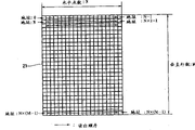
Fig. 3 illustrates the address structure figure of the frame memory 21 of Fig. 1.
As shown in Figure 3, level in array display device 1 is counted to the vertical line number of N/ is in the frame memory 21 of M, writes the pictorial data of 1 picture being read from graphic memory 11 by data read-out control circuit 13 by 0 order to address N * M-1 from the address in the frame memory 21.More particularly, data read-out control circuit 13,0 to address N-1 writes the initial the 1st pictorial data of going from the address, writes the view data of the 2nd row then from address N to address N * 2-1.Write view data of each row equally, write last 1 capablely from address N * (M-1) to address N * M-1, promptly the capable pictorial data of M is finished writing of 1 picture thus.
In addition, the data as once writing frame memory 21 and being read out are not limited to view data, for example, can also be the data that constitute literal etc.And, data transfer rate as frame memory 21, for the mobile phone of the corresponding live image of supporting the IMT-2000 standard, because the present anticipation transfer rate of restriction of data signaling rate etc. is about 15 pictures/second, may be increased to about 30 pictures/second future.
Below with reference to time limit of Fig. 1~3 and Fig. 4 figure, the operation of array display device 1 is described.
Utilize communication function etc. to be input to the view data GD1 of the input control part 10 of array display device 1 from the outside, under the control of data write control circuit 12, once be stored in the graphic memory 11.As shown in Figure 4, when to the process of the view data GD1 of graphic memory 11 storage 1 frame when the time limit, t1 was over, will write the signal WE that is at time limit t1, output to circuit for synchronizing 14 from data write control circuit 12.Write the signal WE circuit for synchronizing 14 that is over and be reset by importing this, and the operation below carrying out.
At circuit for synchronizing 14, receive write the signal WE that is over after, wait for the frame synchronizing signal FS that input is shown in Figure 4, and will read commencing signal RK synchronously with its input time limit t3 and output to data read-out control circuit 13.So by data read-out control circuit 13, be stored in the view data GD1 of graphic memory 11, t3 is read out in the time limit, and is sent to frame memory 21 as view data GD2 temporarily.
On the other hand, in display panel module portion 20, as shown in Figure 4, in refresh cycle based on the reference signal SS (clock signal) that generates by oscillatory circuit 41, be stored in the view data in the frame memory 21, as view data GD3, periodically read by signal electrode driving circuit 23 and be input to signal electrode driving circuit 23.The view data GD3 of per 1 frame of reading from frame memory 21 is numbered as (n) frame by order successively, (n+1) frame, (n+2) frame, later on same incremental value n.The n here is a positive integer.
Display control circuit 42 in the signal electrode driving circuit 23, based on reference signal SS, generation is read control signal RC and is outputed to frame memory 21, and the synchronizing signal of using to decoder circuit 43 output decoders, delta frame synchronizing signal FS and line synchronizing signal LS and output to scan electrode driving circuit 24 simultaneously.Decoder circuit 43 based on from the synchronizing signal of display control circuit 42 and the establishment rule of view data, is decoded into the view data GD3 of input the view data that can image shows with matrix type display board 22.Display panel drive circuit 44 generates and sends control signal to each signal electrode of matrix type display board 22 by decoded view data.Scan electrode driving circuit 24 based on frame synchronizing signal FS and line synchronizing signal LS, generates and sends the control signal to the scan electrode of matrix type display board 22.
As can be seen from Figure 4, the view data GD3 (at time limit t4) that begins to read frame (n+2) usefulness from frame memory 21 before, (at time limit t3) begun view data GD2 from the transmission of graphic memory 11 to frame memory 21, and reads the preceding end that is at the view data GD3 of frame (n+2) usefulness.So, be used as the view data GD3 of frame (n+2) usefulness and the view data GD that reads, always the content that newly is transmitted and stores can not take place from the phenomenon of old view data to the conversion of new view data during reading frame (n+2) from frame memory 21.
And, the time limit t3 that changes according to time limit of frame synchronizing signal FS shown in Figure 4 is to the length of the delay DT1 of time limit t4, the view data GD3 of frame (n+1) usefulness read beginning after, from graphic memory 11 also to the transmission of the view data GD2 of frame memory 21, and, finish in reading of the view data GD3 of frame (n+1) the usefulness back that is over.Therefore, as the view data GD3 of frame (n+1) usefulness and the view data of reading always be transmitted earlier and store, during reading frame (n+1), can not take place from the phenomenon of old view data to the conversion of new view data.
Fig. 5 A~C shows on the matrix type display board 22 in array display device 1, the thick ordinate that moves to right-hand member from left end.
Fig. 5 A~C shows (n) frame, (n+1) frame, (n+2) frame of Fig. 4 respectively.At first such shown in Fig. 5 A, the image of the ordinate 100a of (n) frame is indulged continuously and is shown.
Then, same image data GD3 is read from frame memory 21 once more, and same perpendicular line 100b shows with the frame (n+1) of Fig. 5 B.During reading this frame (n+1), data read-out control circuit 13, beginning writes new view data GD2 to frame memory 21, but because of the address that writes of GD2 lags behind than the address of reading of GD3, so the view data GD2 that newly writes is not read out yet.To writing of the new graph data GD2 of frame memory 21, during following 1 frame (n+2), continued.When GD3 read the address than the writing the address and also lag behind of GD2 the time, then as shown in Figure 5, the new continuous perpendicular line 101b of right shift, shown by new image fully.
Like this, in the array display device 1 of present embodiment 1, because it is synchronous with the frame period of matrix type display board 22, view data GD2 is transmitted to frame memory 21 from graphic memory 11, so that handle and differ as for same address to signal electrode driving circuit 23 reading of view data GD3 handled from frame memory 21 to the transmission of the view data GD2 of frame memory 21, and do not convert midway down at 1 frame of the shown image of matrix type display board 22 that the image control data of 1 frame transmits to for making, therefore, when the show events image, the picture material of the upper and lower of 1 picture can time of origin the displacement phenomenon, thereby can demonstrate level and smooth image.
In embodiment 1, by view data GD2 is synchronous to time limit and frame synchronizing signal FS that the transmission of frame memory 21 begins from graphic memory 11, make and reading view data GD3 midway from frame memory 21, image can not convert the image that newly writes to, but, by signal electrode driving circuit 23, based on frame synchronizing signal FS, when when frame memory 21 is read view data GD3, producing DT1 time delay.For example, when its time delay, DT1 was elongated, the view data GD3 of (n+1) frame among Fig. 4 reads the time limit that is over, be close with the transmission of view data GD2 time limit that is over, when the transmission of view data GD2 be over the time limit when surpassing reading of view data GD3 and being in limited time, 1 frame that image shown on matrix type display board 22 arranged again converts down the possibility of the image of 1 frame to midway.
So the embodiment 2 that below will illustrate will make from DT1 time delay that reads that is sent to image GD3 of view data GD2 not long by adjustment exactly.
Fig. 6 illustrates the structure calcspar of the array display device of embodiments of the present invention 2.
The key distinction of the array display device 2 of Fig. 6 and the array display device 1 of Fig. 1 is to have following delay circuit 30, it is used for the frame synchronizing signal FS that handle is sent by signal electrode driving circuit 23, for with the time limit synchronised that is over of reading of the view data GD3 of any 1 frame, and by the time delay of defined and read, and export as synchronizing signal RS.Other structure of relative assembly, identical with the array display device 1 of embodiment 1 shown in Figure 1, omit no longer explanation at this.
Below, the operation of relevant array display device 2, the time limit figure with reference to Fig. 6 and Fig. 7 does following explanation.
The waveform of GD1 among Fig. 7, WE, FS, GD3 is identical with the corresponding waveform of Fig. 4.Read the waveform of synchronizing signal RS, be by delay circuit 30 make frame synchronizing signal FS and (n+1) frame view data GD3 read the waveform that the time limit t5 that is over postpones the time D T2 of defined synchronously.At time limit t5 with to read synchronizing signal RS synchronous, the transmission of beginning view data GD2.
Because DT1 time delay that reads beginning time limit t4 of the view data GD3 from frame synchronizing signal FS to (n+2) frame is long, can not be directly inputted to circuit for synchronizing 14 to frame synchronizing signal FS, but the synchronizing signal RS that reads after postponing with delay circuit 30 is input to circuit for synchronizing 14, thereby, time delay DT1 become shortened delay circuit 30 time delay DT2 DT3 time delay.In addition, take place synchronously with (n+1) the time limit t5 that is over that reads of the view data GD3 of frame because of reading synchronizing signal RS, so, can avoid the image that on matrix type display board 22, shows 1 frame convert the generation of the phenomenon of 1 two field picture down midway to.
Like this in present embodiment 2, by adding the delay circuit of reading synchronizing signal RS 30 that output makes that frame synchronizing signal FS postpones at the front end of the frame synchronizing signal input part of circuit for synchronizing 14, for example, for response speed is the active array type liquid crystal board of the TFT etc. about 30~50mSec, response speed is the high-speed response type stn liquid crystal plate about 70~80mSec, the organic EL plate of response speed about for number μ Sec etc. has the matrix type display board of different response speeds, owing to can set also as reading the optimal retardation that synchronizing signal RS output delay time can not become oversize by enough delay circuits 30, so no matter be the matrix type display board of that kind, even under the transmission time limit unaccommodated situation of frame synchronizing signal FS, also can demonstrate level and smooth live image as view data GD2 from signal electrode driving circuit 23.
In embodiment 2, by front end at the frame synchronizing signal input part of circuit for synchronizing 14, add a delay circuit 30, be incoming frame synchronizing signal FS, and as make reading of its signal FS and view data GD3 be over time limit t5 synchronous and by optimal delay read the delay circuit that synchronizing signal RS exports, though can avoid image shown on matrix type display board 22 1 frame convert midway down that the phenomenon of the image of 1 frame takes place to, but the clock signal that delay circuit 30 is used might not be identical with signal electrode driving circuit 23 clock internal signals (reference signal SS).
When the used clock signal of reference signal SS and delay circuit 30 not simultaneously because the deviation of each oscillatory circuit can not be set at best retardation with reading synchronizing signal RS sometimes.
So, below in Shuo Ming the embodiment 3, make and read synchronizing signal RS and signal electrode driving circuit 23 clock internal signals (reference signal SS) are synchronous, thereby be not subjected to the influence of oscillatory circuit deviation.
Fig. 8 shows the structure calcspar of the array display device of embodiment of the present invention 3.
The array display device 3 among Fig. 8 and the difference of the array display device 2 among Fig. 6 are to import to delay circuit 31 from the basis increase line of input synchronizing signal LS of the frame synchronizing signal FS of signal electrode driving circuit 23 outputs.In present embodiment 3, be that line synchronizing signal LS is used as the clock signal of delay circuit 31.As for other structure, the same with the array display device 2 of embodiment among Fig. 62, so repeat no more.
Below, for the operation of array display device 3, describe with reference to the time limit figure of Fig. 7 of Fig. 8 and embodiment 2.
When the used clock signal of reference signal SS and delay circuit 30 not simultaneously, then for example the synchronizing signal RS that reads among Fig. 7 becomes inconsistent with (n+1) the time limit t5 that is over that reads of the view data GD3 of frame.So, owing to also become inconsistent, so might appear at the situation of the image that converts down 1 frame midway to of 1 frame of the image that shows on the matrix type display board 22 once more with reading of the view data GD3 time limit t5 that is over reading view data GD2 that synchronizing signal RS is transmitted synchronously.
But, the frame synchronizing signal FS and the line synchronizing signal LS that send from signal electrode driving circuit 23, the reference signal SS that is based on as shown in Figure 2 from identical oscillatory circuit 41 generates, therefore, even if each oscillatory circuit generation deviation does not have a deviation between frame synchronizing signal FS and the line synchronizing signal LS synchronously.
Therefore, in present embodiment 3, as shown in Figure 8, its structure is that line synchronizing signal LS is imported as the clock signal of delay circuit 31.So only come the signal of deferred frame synchronizing signal FS, can be used as and read synchronizing signal RS and from delay circuit 31, export with the umber of pulse of the line synchronizing signal LS of prior setting.At this moment, read synchronizing signal RS and do not have deviation from the retardation of frame synchronizing signal FS, thus (n+1) the view data GD3 of frame read be over time limit t5 and with read synchronizing signal RS synchronously and the view data GD2 that transmits, can be indeed fully synchronously.Therefore, can eliminate the phenomenon that converts following 1 two field picture midway to of 1 frame of the image that on matrix type display board 22, shows.
Like this in present embodiment 3, at line of input synchronizing signal LS on the basis of delay circuit 31 incoming frame synchronizing signal FS, and by coming deferred frame synchronizing signal FS and then output to read synchronizing signal RS as clock line synchronizing signal LS, deviation can not take place because of the deviation of oscillatory circuit etc. in the generation time limit of so reading synchronizing signal RS, can export have an optimal delay amount read synchronizing signal RS, and since can set from frame synchronizing signal FS postpone certain phase mass the optimal delay amount read synchronizing signal RS, so, no matter for example above-mentioned active array type liquid crystal board, high-speed response type stn liquid crystal plate, the kind of the matrix type liquid crystal board of organic EL plate etc., even under the situation that the frequency of oscillatory circuit is drifted about etc. easily, can not be subjected to the influence of the deviation of oscillatory circuit, and can show and stablize level and smooth live image.
And, be under the situation of liquid crystal board at the matrix type display board of each above-mentioned embodiment, can be categorized as transmission-type, reflection-type or Transflective.Transmissive liquid crystal panel needs the interior lighting of bias light etc. for the displaying contents of looking other image, because bias light needs electric power, so be difficult to expect in the mobile information terminal device of mobile phone etc. of low energy consumption.In contrast, reflection-type is owing to being provided with reflecting plate at the whole back side thereby can being used to look other image content displayed from the reflected light of exterior light, so do not need the electric power of bias light, thereby be expected to be used to expect the mobile information terminal device of the mobile phone etc. of low energy consumption.In addition, Transflective is owing to be provided with the reflecting plate of Semitransmissive such as net-point shape overleaf thereby can be used to the displaying contents that reflected light and backlighted both sides from exterior light look other image, so generally speaking, the same electric power that does not need bias light with reflection-type, and just look not in the time of can only externally environment is dark with interior lighting, so not only be expected to be used to expect the mobile information terminal device of the mobile phone etc. of low energy consumption, also owing to improved the degree of looking not in dark occasion, use makes it to be more convenient for.
When the matrix type display board uses the LCD panel of active array type, compare with the LCD panel of the slow STN type of existing response speed, improved response speed and at the contrast of the display part of surrounding environment, even if so live image of the live image of display action fierceness or high-speed mobile, also can demonstrate stable level and smooth live image, and can improve to look and Du not.
When the matrix type display board uses high-speed response type stn liquid crystal display board, compare with the LCD panel of the slow STN type of existing response speed, because improved response speed, so can keep low energy consumption and cheaply under the situation, even if the live image that action is fierce or the live image of high-speed mobile also can show stable, level and smooth image.
When the matrix type display board uses when dynamo-electric glimmering luminescence display panel is arranged, the same with the active array type LCD panel, compare with the LCD panel of the slow STN type of existing response speed, improved response speed.In addition, dynamo-electric glimmering luminescence display panel is arranged, because of the luminous contrast that has improved at the display part of surrounding environment of display part self, so can demonstrate stable, level and smooth live image, and increase because look not when degree compare with liquid crystal, so further improved picture quality, again because do not need bias light, so can realize slimming.
And, when the matrix type display board uses active array type that dynamo-electric glimmering luminescence display panel is arranged, even if when the live image of display action fierceness or the live image of high-speed mobile, also can demonstrate stable, level and smooth live image, and, also because look not when degree compare with liquid crystal and increase, thus picture quality further improved, and can realize slimming.
The invention effect
According to an aspect of the present invention, since with the frame period synchronous images data of matrix display panel from graphic memory, be sent to frame memory, thereby make view data handle to the transmission of frame memory, handle inconsistent in same address from frame memory to reading of signal electrode driving circuit with view data, and then control data transmits so that 1 frame of display image is not converted to the phenomenon of 1 frame down midway on the matrix type display board, therefore, when the show events image, the phenomenon of picture material time of occurrence skew of the upper and lower of one screen picture can not take place, thereby can demonstrate level and smooth image.
According to a further aspect in the invention, according to adding the delay circuit of reading synchronizing signal that output postpones frame synchronizing signal at the front end of the frame synchronizing signal input part of circuit for synchronizing, to various matrix type display boards with different response speeds, can both set also as the optimal delay amount of reading synchronizing signal output delay time length within reason with delay circuit, therefore, except that above-mentioned effect, no matter the kind of all right matrix type display board how, even when being not suitable for as transmission time limit of view data, also can demonstrate level and smooth live image from the frame synchronizing signal of signal electrode driving circuit.
According to a further aspect in the invention, in line of input synchronizing signal again on the basis of delay circuit incoming frame synchronizing signal, thereby feasible line synchronizing signal is exported as the clock delay frame synchronizing signal read synchronizing signal, like this, the generation time limit of reading synchronizing signal can deviation not occur because of the deviation of oscillatory circuit etc., and can export the synchronizing signal of reading with optimal delay amount, and can set from frame synchronizing signal postpone certain phase mass the optimal delay amount read synchronizing signal, therefore except above-mentioned effect, no matter kind that can also the matrix type display board how, even under the situation of easy occurrence frequency drift of pierce circuit etc., also can not be subjected to the deviation effects of oscillatory circuit, can demonstrate stable, level and smooth live image.
According to a further aspect in the invention, because the display board of array display device has used LCD panel, so except above-mentioned effect, can provide low energy consumption and the array display device slim lightweight requirements that satisfies the best that is used for personal digital assistant devices such as mobile phone.
According to a further aspect in the invention, because having used, the display board of array display device do not need backlighted reflective liquid crystal display board, so except that above-mentioned effect, can also provide energy consumption lower array display device.
According to a further aspect in the invention, because the display board of array display device has used and has not needed interior lighting when externally light can utilize, can utilize backlighted Transflective LCD panel when externally environment is dark, therefore, except that above-mentioned effect, also can provide energy consumption array display device lower and easy to use.
According to a further aspect in the invention, because the display board of array display device uses the fast active array type LCD panel of response speed, so except that above-mentioned effect, even if can also provide under the situation of the live image of the live image of display action fierceness or high-speed mobile, also can demonstrate the array display device of live image blur level image little, that image quality is good.
According to a further aspect in the invention, because the display board of array display device uses high-speed response type stn liquid crystal display board, so except that above-mentioned effect, the low-cost of low energy consumption can also be provided, even and under the situation of the live image of the live image of display action fierceness or high-speed mobile, also can demonstrate the array display device of the little image of live image blur level.
According to a further aspect in the invention, because the display board of array display device uses OLED panel, so except above-mentioned effect, can also provide low energy consumption and thin type structure, can demonstrate the array display device that does not almost have the image that moving frame is fuzzy, image quality is good.
According to a further aspect in the invention, because the display board of array display device uses the active matrix organic EL display board, so except that above-mentioned effect, low energy consumption and thin type structure can also be provided, even when the live image of the live image of display action fierceness or high-speed mobile, almost do not have moving frame fuzzy yet, can demonstrate the array display device of the extraordinary image of image quality.
In addition, the active array type liquid crystal board has thin film transistor (TFT) or thin film diode.The active matrix organic EL plate has thin film transistor (TFT).
And the present invention is not limited only to above-mentioned embodiment, in claim scope of the present invention, comprises the feasible more variation of colleague certainly.
Claims (10)
1. array display device, it is made up of following parts, promptly
Display board, it is set in pixel portions by the multiple row signal wire of parallel longitudinal wiring and the fine scanning line of horizontal parallel wiring and arranges on the rectangular point of crossing that forms;
Frame memory, being used for the frame is that the unit storage is presented at the view data on this display board;
The signal electrode driving circuit is used for delta frame synchronizing signal and line synchronizing signal, and, publish picture as data from above-mentioned frame memory read, thereby be generated as the control signal that drives above-mentioned display board signal wire;
Scan electrode driving circuit based on above-mentioned frame synchronizing signal and line synchronizing signal, is generated as the control signal of the sweep trace that drives above-mentioned display board;
Graphic memory is to be the view data that unit stores input temporarily with the frame;
The data write control circuit is control writes a view data from input to this graphic memory;
The data read-out control circuit is that the view data that will be written in the above-mentioned graphic memory is sent on the frame memory,
It is characterized in that:
Above-mentioned data write control circuit, when having write the view data of 1 frame to graphic memory, output writes the signal that is over,
Also comprise circuit for synchronizing, its be used for received above-mentioned write the signal that is over after, based on above-mentioned frame synchronizing signal, above-mentioned data read-out control circuit is output as the commencing signal of reading that the beginning view data transmits.
2. the array display device of record in claim 1 is characterized in that also comprising following delay circuit, promptly
For making from the time limit of above-mentioned graphic memory to the pictorial data transmission of above-mentioned frame memory, ending at above-mentioned signal electrode driving circuit also finishes to read down before 1 frame image data after above-mentioned frame memory is read 1 frame image data, quantitatively postpone above-mentioned frame synchronizing signal by institute, and provide the frame synchronizing signal that is delayed to above-mentioned synchronizing circuit, thus the time limit of reading commencing signal is adjusted.
In claim 2 record array display device, its feature also is:
Above-mentioned delay circuit is that above-mentioned line synchronizing signal is used as clock signal, and the above-mentioned frame synchronizing signal of the pulse daley of being fixed a number by the above line synchronizing signal.
In claim 1 record array display device, its feature also is:
Above-mentioned display board is the LCD panel that is made of liquid crystal display cells.
In claim 4 record array display device, its feature also is:
Above-mentioned LCD panel is the reflective liquid crystal plate by the visual other displaying contents of outside reflection of incident light light.
In claim 4 record array display device, its feature also is:
Above-mentioned LCD panel is the Transflective liquid crystal board by outside reflection of incident light light and the visual other displaying contents of transmitted light.
In claim 4 record array display device, its feature also is:
Above-mentioned LCD panel is the active array type liquid crystal board.
In claim 4 record array display device, its feature also is:
Above-mentioned LCD panel has been to use the liquid crystal board of high-speed response type supertwist birefringence mode element.
In claim 1 record array display device, its feature also is:
Above-mentioned display board is that dynamo-electric glimmering luminous plaque is arranged.
In claim 9 record array display device, its feature also is:
Described have a dynamo-electric glimmering luminous plaque, is that active array type has dynamo-electric glimmering luminous plaque.
Applications Claiming Priority (3)
| Application Number | Priority Date | Filing Date | Title |
|---|---|---|---|
| JP293760/2000 | 2000-09-27 | ||
| JP293760/00 | 2000-09-27 | ||
| JP2000293760A JP3611511B2 (en) | 2000-09-27 | 2000-09-27 | Matrix type display device, image data display method, and portable information terminal device |
Publications (2)
| Publication Number | Publication Date |
|---|---|
| CN1347069A CN1347069A (en) | 2002-05-01 |
| CN1157703C true CN1157703C (en) | 2004-07-14 |
Family
ID=18776494
Family Applications (1)
| Application Number | Title | Priority Date | Filing Date |
|---|---|---|---|
| CNB011411015A Expired - Fee Related CN1157703C (en) | 2000-09-27 | 2001-09-27 | Array display device |
Country Status (5)
| Country | Link |
|---|---|
| US (1) | US6700571B2 (en) |
| EP (1) | EP1193671B1 (en) |
| JP (1) | JP3611511B2 (en) |
| CN (1) | CN1157703C (en) |
| DE (1) | DE60105365T2 (en) |
Families Citing this family (24)
| Publication number | Priority date | Publication date | Assignee | Title |
|---|---|---|---|---|
| FI115802B (en) * | 2000-12-04 | 2005-07-15 | Nokia Corp | Refresh the photo frames on the memory display |
| US7009604B2 (en) * | 2002-07-19 | 2006-03-07 | Sun Microsystems, Inc. | Frame detector for use in graphics systems |
| KR100490420B1 (en) * | 2002-12-26 | 2005-05-17 | 삼성전자주식회사 | Apparatus and method for generating programmable drive signal in display panel |
| JP2004226522A (en) * | 2003-01-21 | 2004-08-12 | Hitachi Displays Ltd | Display device and driving method therefor |
| EP1600917A4 (en) * | 2003-02-25 | 2007-11-07 | Mitsubishi Electric Corp | Matrix type display device and display method thereof |
| JP4393106B2 (en) * | 2003-05-14 | 2010-01-06 | シャープ株式会社 | Display drive device, display device, and portable electronic device |
| KR100580177B1 (en) * | 2003-09-22 | 2006-05-15 | 삼성전자주식회사 | Display synchronization signal generation apparatus in the digital receiver, decoder and method thereof |
| US8466924B2 (en) | 2004-01-28 | 2013-06-18 | Entropic Communications, Inc. | Displaying on a matrix display |
| JP2006030389A (en) * | 2004-07-13 | 2006-02-02 | Alpine Electronics Inc | Information processor, system, display method, and program |
| KR100582402B1 (en) * | 2004-09-10 | 2006-05-22 | 매그나칩 반도체 유한회사 | Method and TDC panel driver for timing control to erase flickers on the display panel |
| JP2006174363A (en) * | 2004-12-20 | 2006-06-29 | Nec Electronics Corp | Frame synchronizer, optical disk drive, information recording/reproducing device, and signal synchronizing method |
| DE102006003531A1 (en) * | 2006-01-24 | 2007-08-02 | Schott Ag | Transporting, homogenizing and/or conditioning glass melt comprises adjusting residence time of melt in transporting and/or conditioning device using section of wall of device |
| JP2007248965A (en) * | 2006-03-17 | 2007-09-27 | Yazaki Corp | Graphic display device and graphic display method |
| KR100805610B1 (en) * | 2006-08-30 | 2008-02-20 | 삼성에스디아이 주식회사 | Organic light emitting display device and driving method thereof |
| JP2008216362A (en) * | 2007-02-28 | 2008-09-18 | Optrex Corp | Driving device for display apparatus |
| JP5242076B2 (en) * | 2007-04-13 | 2013-07-24 | グローバル・オーエルイーディー・テクノロジー・リミテッド・ライアビリティ・カンパニー | Active matrix display device |
| JP5407137B2 (en) * | 2007-11-22 | 2014-02-05 | 日亜化学工業株式会社 | Lighting device, lighting unit |
| JP5399163B2 (en) | 2009-08-07 | 2014-01-29 | グローバル・オーエルイーディー・テクノロジー・リミテッド・ライアビリティ・カンパニー | Display device |
| JP5508836B2 (en) | 2009-12-24 | 2014-06-04 | 株式会社メガチップス | Setting control apparatus and operation method of setting control apparatus |
| JP5606746B2 (en) * | 2010-01-27 | 2014-10-15 | 京セラ株式会社 | Mobile terminal device |
| KR101861723B1 (en) | 2011-12-20 | 2018-05-30 | 삼성전자주식회사 | Devices and method of adjusting synchronization signal preventing tearing and flicker |
| JP2014052548A (en) * | 2012-09-07 | 2014-03-20 | Sharp Corp | Memory controller, portable terminal, memory control program and computer readable recording medium |
| KR102456654B1 (en) | 2014-11-26 | 2022-10-18 | 가부시키가이샤 한도오따이 에네루기 켄큐쇼 | Display device and electronic device |
| CN114281295B (en) * | 2020-09-18 | 2024-03-15 | 西安诺瓦星云科技股份有限公司 | Image processing method and device and LED display screen system |
Family Cites Families (11)
| Publication number | Priority date | Publication date | Assignee | Title |
|---|---|---|---|---|
| US5095301A (en) * | 1985-11-06 | 1992-03-10 | Texas Instruments Incorporated | Graphics processing apparatus having color expand operation for drawing color graphics from monochrome data |
| EP0525986B1 (en) * | 1991-07-26 | 1996-11-13 | Sun Microsystems, Inc. | Apparatus for fast copying between frame buffers in a double buffered output display system |
| DE4231158C5 (en) * | 1991-09-17 | 2006-09-28 | Hitachi, Ltd. | Method and device for the composition and display of images |
| JP3582082B2 (en) | 1992-07-07 | 2004-10-27 | セイコーエプソン株式会社 | Matrix display device, matrix display control device, and matrix display drive device |
| JPH06282643A (en) * | 1993-03-29 | 1994-10-07 | Matsushita Electric Ind Co Ltd | Picture synthesizing effect device |
| US5446496A (en) * | 1994-03-31 | 1995-08-29 | Hewlett-Packard Company | Frame rate conversion with asynchronous pixel clocks |
| WO1996007175A1 (en) * | 1994-08-31 | 1996-03-07 | S3 Incorporated | Apparatus for correction of video tearing |
| JP3307807B2 (en) * | 1995-09-29 | 2002-07-24 | 三洋電機株式会社 | Video signal processing device |
| JPH1195728A (en) | 1997-09-25 | 1999-04-09 | Hitachi Ltd | Liquid crystal display controller |
| JP3811251B2 (en) | 1997-04-24 | 2006-08-16 | 旭硝子株式会社 | Driving device for liquid crystal display device |
| KR100613438B1 (en) * | 1999-11-17 | 2006-08-18 | 엘지.필립스 엘시디 주식회사 | Transflective liquid crystal display device and method for fabricating the same |
-
2000
- 2000-09-27 JP JP2000293760A patent/JP3611511B2/en not_active Expired - Fee Related
-
2001
- 2001-09-24 DE DE60105365T patent/DE60105365T2/en not_active Expired - Lifetime
- 2001-09-24 EP EP01308110A patent/EP1193671B1/en not_active Expired - Lifetime
- 2001-09-26 US US09/962,166 patent/US6700571B2/en not_active Expired - Lifetime
- 2001-09-27 CN CNB011411015A patent/CN1157703C/en not_active Expired - Fee Related
Also Published As
| Publication number | Publication date |
|---|---|
| US6700571B2 (en) | 2004-03-02 |
| DE60105365T2 (en) | 2005-09-29 |
| JP3611511B2 (en) | 2005-01-19 |
| EP1193671A2 (en) | 2002-04-03 |
| DE60105365D1 (en) | 2004-10-14 |
| JP2002108268A (en) | 2002-04-10 |
| EP1193671B1 (en) | 2004-09-08 |
| US20020041277A1 (en) | 2002-04-11 |
| CN1347069A (en) | 2002-05-01 |
| EP1193671A3 (en) | 2003-04-23 |
Similar Documents
| Publication | Publication Date | Title |
|---|---|---|
| CN1157703C (en) | Array display device | |
| CN1186757C (en) | Driving circuit and method for indicator and the indicator | |
| CN1197046C (en) | Electrooptical screen and its drive method, electrooptical apparatus and electronic equipment | |
| CN1261806C (en) | Liquid-crystal display device and driving method thereof | |
| TWI292899B (en) | Liquid crystal display device and driving method to be used in same | |
| CN1272654C (en) | LCD equipment having improved precharge circuit and method of driving same | |
| CN1159692C (en) | Digital driver circuit for electro-optical device and electro-optical device digital driver circuit | |
| CN101887197B (en) | Liquid crystal display | |
| CN1162831C (en) | Display control method, display controller, display unit and electronic device | |
| CN100538454C (en) | Liquid Crystal Display And Method For Driving | |
| CN1360297A (en) | Liquid crystal display, drive circuit, drive method and electronic apparatus | |
| CN101055359A (en) | Semi-penetration/ reflection liquid crystal display and its production method | |
| CN1740858A (en) | The panel of LCD that comprises gate drivers | |
| CN1577482A (en) | Display device and driving method thereof | |
| CN101046941A (en) | Apparatus and method for driving liquid crystal display device | |
| CN1847936A (en) | Display device | |
| CN102737602A (en) | Liquid crystal display device and display control method | |
| CN1655220A (en) | Electro-optical device, driving method of electro-optical device, driving circuit of electro-optical device and electronic apparatus | |
| KR20140127318A (en) | Display device, electronic device comprising same, and drive method for display device | |
| WO2013190912A1 (en) | Liquid crystal display device, electronic apparatus provided therewith, and method for driving liquid crystal display device | |
| TWI301258B (en) | Driving system for matrix type backlight module | |
| CN1280354A (en) | Display device and its driving method | |
| CN1732498A (en) | Semiconductor device, light-emitting display device and driving method thereof | |
| JP2004233932A (en) | Liquid crystal display | |
| JPH11194749A (en) | Liquid crystal display device and driving method therefor |
Legal Events
| Date | Code | Title | Description |
|---|---|---|---|
| C10 | Entry into substantive examination | ||
| SE01 | Entry into force of request for substantive examination | ||
| C06 | Publication | ||
| PB01 | Publication | ||
| C14 | Grant of patent or utility model | ||
| GR01 | Patent grant | ||
| CF01 | Termination of patent right due to non-payment of annual fee | ||
| CF01 | Termination of patent right due to non-payment of annual fee |
Granted publication date: 20040714 Termination date: 20180927 |