EP1192474B1 - Floating plate voltage monitor - Google Patents
Floating plate voltage monitor Download PDFInfo
- Publication number
- EP1192474B1 EP1192474B1 EP00930129A EP00930129A EP1192474B1 EP 1192474 B1 EP1192474 B1 EP 1192474B1 EP 00930129 A EP00930129 A EP 00930129A EP 00930129 A EP00930129 A EP 00930129A EP 1192474 B1 EP1192474 B1 EP 1192474B1
- Authority
- EP
- European Patent Office
- Prior art keywords
- voltage
- ion
- amplifier
- ion conducting
- conducting surface
- Prior art date
- Legal status (The legal status is an assumption and is not a legal conclusion. Google has not performed a legal analysis and makes no representation as to the accuracy of the status listed.)
- Expired - Lifetime
Links
- 238000007667 floating Methods 0.000 title claims abstract description 23
- 238000012544 monitoring process Methods 0.000 claims abstract description 34
- 238000000034 method Methods 0.000 claims abstract description 16
- 239000003990 capacitor Substances 0.000 claims description 31
- 239000004020 conductor Substances 0.000 claims description 13
- 239000011810 insulating material Substances 0.000 claims description 3
- 150000002500 ions Chemical class 0.000 description 133
- 238000012360 testing method Methods 0.000 description 24
- 238000005259 measurement Methods 0.000 description 17
- 239000004065 semiconductor Substances 0.000 description 16
- 239000000523 sample Substances 0.000 description 14
- 238000010586 diagram Methods 0.000 description 10
- 125000006850 spacer group Chemical group 0.000 description 7
- 238000004519 manufacturing process Methods 0.000 description 5
- 230000000694 effects Effects 0.000 description 4
- 229910052751 metal Inorganic materials 0.000 description 4
- 239000002184 metal Substances 0.000 description 4
- 238000009825 accumulation Methods 0.000 description 3
- 238000000429 assembly Methods 0.000 description 3
- 230000000712 assembly Effects 0.000 description 3
- 230000008859 change Effects 0.000 description 3
- 238000010276 construction Methods 0.000 description 3
- 230000006870 function Effects 0.000 description 3
- 230000008569 process Effects 0.000 description 3
- 230000004044 response Effects 0.000 description 3
- 230000008901 benefit Effects 0.000 description 2
- 230000008878 coupling Effects 0.000 description 2
- 238000010168 coupling process Methods 0.000 description 2
- 238000005859 coupling reaction Methods 0.000 description 2
- 238000013480 data collection Methods 0.000 description 2
- 230000001419 dependent effect Effects 0.000 description 2
- 239000003989 dielectric material Substances 0.000 description 2
- 230000009977 dual effect Effects 0.000 description 2
- 239000010408 film Substances 0.000 description 2
- 238000009413 insulation Methods 0.000 description 2
- 239000012774 insulation material Substances 0.000 description 2
- 238000012423 maintenance Methods 0.000 description 2
- 239000000463 material Substances 0.000 description 2
- 230000009467 reduction Effects 0.000 description 2
- 230000001105 regulatory effect Effects 0.000 description 2
- 229910001369 Brass Inorganic materials 0.000 description 1
- 229910052782 aluminium Inorganic materials 0.000 description 1
- XAGFODPZIPBFFR-UHFFFAOYSA-N aluminium Chemical compound [Al] XAGFODPZIPBFFR-UHFFFAOYSA-N 0.000 description 1
- 238000004458 analytical method Methods 0.000 description 1
- 238000013459 approach Methods 0.000 description 1
- 238000003491 array Methods 0.000 description 1
- 239000010951 brass Substances 0.000 description 1
- 238000004140 cleaning Methods 0.000 description 1
- 238000004891 communication Methods 0.000 description 1
- 230000006378 damage Effects 0.000 description 1
- 238000013500 data storage Methods 0.000 description 1
- 230000001934 delay Effects 0.000 description 1
- 238000000151 deposition Methods 0.000 description 1
- 238000001514 detection method Methods 0.000 description 1
- 230000005684 electric field Effects 0.000 description 1
- 230000005686 electrostatic field Effects 0.000 description 1
- 230000008030 elimination Effects 0.000 description 1
- 238000003379 elimination reaction Methods 0.000 description 1
- 230000005284 excitation Effects 0.000 description 1
- 239000004973 liquid crystal related substance Substances 0.000 description 1
- 230000004048 modification Effects 0.000 description 1
- 238000012986 modification Methods 0.000 description 1
- 230000003287 optical effect Effects 0.000 description 1
- 230000001681 protective effect Effects 0.000 description 1
- 230000003252 repetitive effect Effects 0.000 description 1
- 238000004088 simulation Methods 0.000 description 1
- 239000007787 solid Substances 0.000 description 1
- 239000010409 thin film Substances 0.000 description 1
- 230000007704 transition Effects 0.000 description 1
Images


Classifications
-
- G—PHYSICS
- G01—MEASURING; TESTING
- G01R—MEASURING ELECTRIC VARIABLES; MEASURING MAGNETIC VARIABLES
- G01R29/00—Arrangements for measuring or indicating electric quantities not covered by groups G01R19/00 - G01R27/00
- G01R29/24—Arrangements for measuring quantities of charge
-
- G—PHYSICS
- G01—MEASURING; TESTING
- G01R—MEASURING ELECTRIC VARIABLES; MEASURING MAGNETIC VARIABLES
- G01R19/00—Arrangements for measuring currents or voltages or for indicating presence or sign thereof
- G01R19/0046—Arrangements for measuring currents or voltages or for indicating presence or sign thereof characterised by a specific application or detail not covered by any other subgroup of G01R19/00
- G01R19/0061—Measuring currents of particle-beams, currents from electron multipliers, photocurrents, ion currents; Measuring in plasmas
Definitions
- This invention relates the art of electrical measurements, and more particularly to an electrical measuring method and apparatus which provides for the voltage measurement and pre-charging of an isolated and/or remote surface or structure such as the ion collecting plate element of a floating plate ion monitoring system.
- Floating plate ion monitoring systems are typically used to measure the effectiveness and efficiency of room air ionization systems employed in the semiconductor manufacturing process industry to reduce or eliminate charge accumulation on charge sensitive semiconductor or LCD (liquid crystal devices) during the manufacturing process.
- LCD liquid crystal devices
- charge accumulation on charge sensitive semiconductor elements such as mosfet gates arrays,, digital memory or logic elements, or LCD devices using TFT device (thin film transistors), if not controlled or eliminated will cause immediate destruction or early life field failure of the semiconductor junctions of these devices.
- TFT device thin film transistors
- Air ions both positive and negative, are typically used to flood areas where semiconductor devices are being processed to provide a pool of mobile air ion charges which can be attracted by the undesirable charges associated with the semiconductor devices under process to effectively cancel them to zero ,net charge.
- the typical floating plate ion monitoring system plays an important role in the air ion control system by providing a means of measuring the quantity of mobile air ions of each polarity being produced by an air ionization system, as well as providing a measure of the ability of the produced air ion field to hold various spatial areas associated with the semiconductor process line at a zero or near zero voltage level.
- the typical floating plate monitoring system provides two modes of operation, a "decay” mode and a "float” mode.
- the ion collecting plate or surface associated with the monitor is pre-charged to a positive or negative voltage level of typically 1000 volts or more.
- the time required for the collecting plate to be discharged to a level of 10% of the starting value, i.e. 100 volts, by ion impingement from the ion field is measured by a timer in the monitor to indicate the quantity of either polarity of air ion associated with the ion field.
- This measurement is done with a pre-charge level of positive 1000 volts to indicate the quantity of negative air ions or with a pre-charge level of negative 1000 volts to indicate the quantity of positive air ions. In either case the time required for the plate to be discharged to a 100 volt level by the attraction of the oppositely charged air ion to the ion collecting plate is measured and used to indicate the "richness" of the particular ion in the field.
- the ion collecting plate In the float mode the ion collecting plate is initially preset to a zero voltage level and then allowed to "float" to a voltage level dictated by the impingement of incident ions from the ion field.
- the float measurement indicates the effectiveness of the field in reducing the net charge on the semiconductor devices to a low value while also indicating to what voltage level all devices, even devices which were not initially charged, will be driven to by the ion field.
- Floating plate monitoring systems heretofore available suffer from many disadvantages.
- electrostatic voltmeter probes typically of the field "mill” or tuning fork chopper types, are expensive and require a large mounting space at the ion collecting plate assembly to effectively read the plate voltage.
- a relay or solenoid is typically used to momentarily connect the plate to a pre-charge level voltage source. This requires a low leakage relay scheme to maintain the plate at a high impedance level relative to ground thus typically requiring the relay to be positioned at the ion collecting plate structure itself.
- Another disadvantage is that to operate the ion collection plate assembly a large diameter connecting cable to the monitor electronic assembly is typically used to accommodate the wiring for the electrostatic probe device electronics, the HV relay device actuation wiring, the high voltage wiring for the pre-charge supply and the ground reference connection for the ground reference element. This results in a bulky ion collecting plate assembly cable which limits assembly position flexibility and easy placement of the assembly.
- a further disadvantage is that whereas it is desirable to construct an ion collection plate which is of the same relative size and thickness as the semiconductor devices which are placed within the ion field, the current art ion collecting elements, due to their required size to accommodate the required relay, electrostatic probe, and required measurement capacitance, cannot be constructed in the size desired.
- Another disadvantage is that to produce the required ion collecting plate capacitance relative to the ground referenced element precise manufacturing of the ion collecting plate is required while other mechanical components such as spacers to support the ion collecting plate element from the ground reference element must be of high precision, low leakage and high cost construction.
- a still further disadvantage is that the bandwidth (frequency response) of current art floating plate monitoring systems is limited to approximately 40 to 50Hz due to the use of the typical electrostatic probe system used to monitor the ion collecting plate. This is a serious limitation particularly where A.C. type air ion production equipment is employed. The A.C. type ion production equipment can induce damaging A.C. fields and voltages at the location of the semiconductor devices and cannot be accurately measured using current art type floating plate monitors.
- US-A-4370616 discloses a low impedance electrostatic detector comprising a detector electrode sensitive to electrostatic quantities, means for varying the capacitive coupling between the electrode and the electrostatic quantity to which the electrode is exposed, and an operational amplifier having an output and a pair of inputs, one of which is operationally associated with the amplifier summing mode.
- EP-A-0222950 discloses a non-contact auto-ranging electrostatic field meter with automatic distance indicator.
- Preferred embodiments eliminate the necessity and use of the typical electrostatic voltage probe in the ion plate assembly construction.
- Preferred embodiments eliminate the necessity and use of a high voltage relay or solenoid in the ion plate assembly construction.
- Preferred embodiments eliminate the requirement of providing an ion collecting plate structure which is dependent upon mechanical considerations such as plate area and plate spacing, both relative to the ground reference structure, to establish the specified ion plate capacitance to the ground reference, but to establish the specified capacitance using electrical means.
- Preferred embodiments reduce the connecting cable to the ion collecting plate structure to a highly flexible small diameter cable to allow easy positioning of the ion plate assembly to the areas of measurement by the use of a single conductor shielded cable.
- Preferred embodiments provide a high bandwidth capability floating plate voltage monitoring system to allow for the detection and measurement of A.C. electrical fields which are in the vicinity of the ion collector plate.
- Preferred embodiments provide a technique whereby an isolated surface or structure may be charged to a given voltage level during a "charge” sequence while the voltage level of the isolated surface or structure can be monitored during a "read” sequence using a single shielded conductor to the floating plate assembly to charge, discharge and monitor the ion collection surface or structure.
- Preferred embodiments provide a technique whereby an isolated surface or structure can be shielded from extraneous electrostatic charges, voltages, or fields on as many sides of the surface or structure as desired while maintaining very low capacitive loading or resistive loading due to leakage from the ion collecting surface to the shielding electrode or by the capacitance or leakage effects of the connecting cable.
- Preferred embodiments provide a technique which will allow the ion collector plate assembly to be operated without the use of an electrostatic probe device, a relay device, and/or a bulky cable so as to allow the assembly to be constructed in various sizes and thicknesses which are comparable to the size and thickness of various semiconductor devices which are being processed to provide for high accuracy simulation by the floating plate monitoring system of the response of the semiconductor devices to the ion field and/or A.C. field.
- Preferred embodiments provide a floating plate monitoring system which requires low maintenance and features high reliability by eliminating the use of mechanical devices such as electrostatic probes and relays or solenoids.
- the present invention provides a floating plate ion monitoring system as defined in claim 1 and a floating plate ion monitoring system as defined in claim 14.
- the system comprises : an ion collector assembly comprising an ion conducting surface and a shielding surface in spaced relation, the ion conducting surface being located to receive ion impingement thereon; and a voltage follower circuit electrically connected to the ion conducting surface and to the shielding surface for applying to the shielding surface a potential which duplicates and follows the voltage appearing on the ion conducting surface; a capacitance connected to the ion conducting surface so that the capacitance between the ion conducting surface and the shielding surface is established electrically and independent of the physical configuration of the ion collector assembly; and a circuit for applying an electrical reference to the connected capacitance so that the voltage rating thereof need not be equal to or greater than the limits of voltage appearing in operation on the ion conducting surface.
- the foregoing may be accomplished by providing a unity gain connected operational amplifier and connecting the positive input thereof to the ion conducting surface and the inverting input thereof to the shielding surface.
- An indicator connected to the amplifier output monitors the voltage on the ion conducting surface.
- a voltage reference is applied to the electrically established capacitance so that the voltage rating thereof need not be equal to or greater than the limits of voltage appearing on the ion conducting surface.
- the magnitude of the applied voltage reference can be varied in a manner varying the magnitude of the electrically established capacitance.
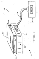
- Fig. 1 Shown in Fig. 1 is a pictorial representation of a typical current art floating plate ion monitoring system 10.
- the ion collecting plate assembly 12 is shown connected via cable 14 to the monitor electronics assembly 16.
- the ion collector plate 20 typically has 20 the dimensions of 15cm on a side for an area 225cm 2 and is spaced away from the ground referenced structure 22 by approximately 2.5cm as established by four low leakage spacers 24 to establish a capacitance between surface 20 and ground reference structure 22 of 20pf +/-10% as required by the measurement standard.
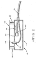
- FIG. 2 Shown in Fig. 2 is a pictorial representation of the ion collector plate assembly 12 with the ground reference structure 22 shown in cutaway to illustrate the electrostatic probe 30 supported by mounting means 32 so as to capacitively couple probe 30 to measure the voltage of the surface 34 ion collecting plate 20, through an aperture 36. Also shown is a solenoid 38 which, when energized, makes contact to surface 34 to apply a voltage to surface 34 to pre-charge the surface for decay mode operation measurements or discharge it to zero for float mode operation.
- Cable 14 contains the wiring for the electronics of probe 30 which includes the probe modulator excitation signals, the signal output and power supply connections. Cable 14 also includes wiring for the ground reference structure 22, the solenoid actuation signal, and the pre-charge bias level supply.
- Fig. 3A Shown in Fig. 3A is a schematic and pictorial representation of the ion collecting plate assembly 50.
- Fig. 3B is a plan view of the top of the assembly, i.e. the ion collection surface 52 on a supporting surface 54.
- the dimensions of surface 52 are shown as S1 and S2 which can be of any desired dimensions consistent with the desired application. Variations may include rectangular, circular, or any other combination of shapes or sizes.
- surface 52 does not have to be flat but can take various shapes such as spherical or conical.
- Surface 52 to perform as an ion collection surface, is preferably a conduction surface, such as metal or a semiconducting surface with a surface and/or volume resistivity ranging up to approximately 10 8 -10 10 ohm/square.
- Surface 52 therefore can be provided by the use of a metal plate of flat or formed conducting material such as aluminum or brass or it may be provided by a conductive or semi-conductive film either rigid or flexible which can be bonded, deposited or evaporated onto the support surface 54, an insulating material.
- the term "ion conducting surface” therefore includes the various forms of surface 52. In the case where surface 52 is a rigid surface or structure, no support surface 54 is required and discreet spacers may be employed.
- Assembly 50 also includes a shielding surface 62, preferably a conductive surface which functions to shield surface 52 from electrostatic influences, such as voltage, charge or fields which may attempt to couple to surface 52 from either the bottom or sides of the assembly.
- the size and shape of shielding surface 62 is consistent with the size and shape of surface 52 to allow surface 62 to shield surface 52 against extraneous coupling to undesired sources.
- shielding surface 62 does not connect to ground reference but has a voltage applied to it which duplicates and follows the voltage appearing on the ion collecting surface 52, the purpose of which will be explained presently.
- surface 52 has the capability to experience a voltage range of ⁇ 1000 volts or more, surface 62 will be driven to follow the same voltage extremes as may appear on ion collecting surface 52.
- Surface 62 therefore should be insulated on its bottom side to prevent arc-over to grounded or other surfaces which may come into close proximity to it. Therefore surface 64, shown in relation to surface 62, is an insulating surface, to provide the needed insulation. Insulating jacket 66 is used to cover shielded cable 68 to prevent arc-over from the cable shield 70 to grounded objects.
- the thickness dimension of the ion collecting assembly 50 can be of any desired value to accommodate many applications.
- the spacing between insulating surface 54, if used, and shielding surface 62 could be dictated by the thickness of surface 54 if, for example, surface 52 and surface 62 are made by depositing or bonding a metal film on each side of surface 54.
- This dual sided bonded metal structure could be constructed easily using standard dual sided printed circuit board material which is inexpensive and easily obtainable.
- two pieces of single sided printed circuit board material could be used to construct the entire assembly by using one piece of single sided printed circuit board to form insulating surface 64 and shielding surface 62 and the other piece used for insulating surface 54 and ion collecting surface 52.
- the two pieces could be either bonded together if very thin assemblies are required, or spaced apart relative to each other by discreet spacers or other insulating material if thicker assemblies are desired.
- a primary objective of the present invention is to eliminate the effect of the physical configuration of the ion collecting plate assembly 50 on the capacitance between ion collecting surface 52 and shielding surface 62 as well as the capacitive loading effect of the connecting cable 68.
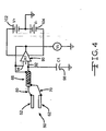
- the connection of the ion collecting plate assembly 50 via a cable 68 into the apparatus shown schematically in Fig. 4 will accomplish this objective.
- Fig. 4 there is a simplified representation of the ion collecting plate assembly 50 including the ion collecting surface 52 and the shielding surface 62 connected to a unity gain connected, i.e. buffer, operational amplifier 90.
- surface 52 is connected via the center conductor 80 of the shielded cable 68 to the input terminal 92, also designated (+) of amplifier/buffer 90.
- the shielding surface 62 and the shield of cable 70 are connected to the output and inverting input 94, also designated (-) of the amplifier/buffer 90.
- the output of amplifier 90 will be a voltage which will follow closely the voltage applied to the input 92 (+) with a gain which approaches unity (i.e. 0.99999).
- the capacitance between surface 52 and surface 62 is 100 picofarads, while the capacitance of cable 68 between its center conductor 80 and its shield 70, being nominally 25 picofarads per foot and, for example, for a 10 foot length of cable being 250 picofarads, the total physical capacitance would be 350 picofarads.
- the resistive leakage current between the ion collecting surface 52 and the shielding surface 62 and the resistive leakage current between the center conductor 80 and the shield 70 of shielded cable 68 are both driven to a very low value due to the zero voltage difference therebetween. Therefore, the use of expensive low leakage insulation material for insulating surface 54 and/or insulating spacers, if used, or cable dielectric material, is not required.
- Cl sets the capacitance of the ion collecting surface 52 to ground by electrical means and makes the mechanical capacitance of the ion collecting plate assembly (and the cable capacitance) negligible, which is an objective of this invention.
- the circuit of Fig. 4 also includes bias voltage sources 102 and 104 connected to amplifier 90 and an indicator, such as a voltmeter 106, connected between the output of amplifier 90 and ground.
- the voltage-follower technique provides virtually infinite impedance loading of the ion collecting plate assembly 50 while allowing the plate to be charged and monitored through the same small diameter cable. Therefore, the size and shape of the ion conducting plate assembly 50 and its capacitance to ground may be tailored to a particular requirement. For example, the plate capacitance can be matched to the capacitance of a particular ESD-sensitive device, or the plate dimensions can be made to permit placement of the plate assembly 50 in a remote or restricted place.
- the circuit of Fig. 4 is limited in monitoring voltages on ion collecting surface 52 to a range dictated by the voltage range capability of the amplifier/buffer 90 and is typically in the range of ⁇ 30 volts for monolithic structure amplifiers.
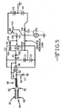
- the circuitry shown in Fig. 5 can be used to expand the ion plate voltage measurement range to cover high voltages up to the limits dictated by the capability of transistor Q1, also designated 110, with its supply voltages of V3 and V4.
- Other high voltage regulating schemes can also be applied such as the use of cascoded bipolar or F.E.T. devices, use of high voltage photocells, or step-up regulating switching transformers etc. to obtain voltages ranges into the kilovolt range as required.
- the particular voltage expanding scheme shown in Fig. 5 operates in the following manner.
- the voltage of the driven feedback line 120 is controlled by transistor Q1. For example, if Q1 turns fully off, the V4 supply pulls the driven feedback line 120 fully to the V4 supply through resistor 122, also designated R4. If Q1 turns fully on to a current equal to V3-V4 divided by R4, the driven feedback line 120 is pulled to the V3 supply value.
- Various degrees of current through Q1 cause various voltage levels of the driven feedback line 120 within the limits set by V3 and V4.
- An operational amplifier 128, also designated A2, compares the voltage difference between the driven feedback line 120 and the output of amplifier/buffer 90 at point A and controls the amount of current through Q1. Therefore, amplifier A2 controls the voltage level of the driven feedback line 120.
- the output of amplifier/buffer 90 at point A rises above the voltage on the driven feedback line 120
- the output of amplifier A2 integrates negatively to increase the emitter current of Q1 through resistor 130, also designated R3, to a value which causes the driven feedback voltage to increase to re-establish a zero voltage difference between the voltage at point A and the driven feedback line 120.
- This same process of nulling the voltage difference between the output voltage of amplifier/buffer 90 and the voltage of the driven feedback line 120 to zero will occur for any voltage output of amplifier/buffer 90 which is within the voltage limits established V3 and V4.
- V3 and V4 The connection of the center tap of supplies V1 and V2 to the driven feedback line 120 will provide the proper operating voltage supplies for amplifier/buffer 90 and operational amplifier A2.
- the limits of V3 and V4 would be in the order of 500 volts each with Q1 chosen to be capable of a 1000 volt VCE stress.
- Q1 would be cascaded to a 2000 volts VCE stress capability and both V3 and V4 increased to 1000 volts each.
- the value of R4 would be in the range of 1 to 10 megohms, R3 would be selected to provide up to approximately 2ma and would be 5 kilohms for a -10 volts output from A2.
- R1, C2, and R2 also designated 132, 134 and 136, respectively, are selected to provide high bandwidth with stable operation and are 10 kilohms, 1000 picofarads and 1 kilohms, respectively.
- Vo, the output indicator 140 could be connected to the driven feedback line 120, as shown, or to the output of amplifier/buffer 90 as previously shown in Fig. 4 due to the zero voltage between these points.
- the voltage expanding amplifier section could take many forms including the use of high voltage optical couplers, active semiconductor devices in place of R4, etc., the circuit of Fig. 5 being one of the simplest.
- Fig. 6 Shown in Fig. 6 , is the circuit as shown in Fig. 5 with added elements D1, D2, S1, and V B , a voltage supply.
- the purpose of the added components is to accomplish the objective of providing a means to eliminate the use of a relay or solenoid to change the ion collecting surface 52 to a pre-set level, say plus or minus 1 kilovolt, for operation of the monitor in the decay mode.
- Diodes D1 and D2, also designated 150 and 152 are low capacitance, low leakage types which will not allow the voltage difference between the input connection 92 (+input) of amplifier/buffer 90 (A1) and the driven feedback line 120 to exceed plus or minus approximately 0.5 volts.
- the voltage difference between the input of amplifier/buffer 90 (A1) (+) and the driven feedback line would normally be driven to zero. Therefore, for this normal operating case the diodes D1 and D2 are "transparent" and have no function in the circuit except to provide protection for the input of amplifier/buffer 90 (A1) if a voltage were applied to the ion collecting surface 52 which exceeded the linear operating voltage of the monitor as established by V3 and V4. For this over voltage situation D1 and D2 would conduct current from surface 52 into the driven feedback line to protect the input circuit of amplifier/buffer 90 (A1).
- switch S1 When switch S1, also designated 156, is in the "read” position the circuit of Fig. 6 is identical to the circuit of Fig. 5 except for the addition of diodes D1 and D2.
- V B a voltage supply, also designated 158, is connected into the input of amplifier (A2) at point A while disconnecting the output of amplifier/buffer (A1) from the amplifier/buffer (A2) input circuit. This will cause the driven feedback line 120 to be driven to the potential of V B rather than to the potential of the output of amplifier/buffer (A1).
- V B may be chosen to be plus or minus any voltage within the linear voltage range of the monitor as established by V3 and V4.
- switch S1 is returned to the "read” position to again monitor the output voltage of amplifier/buffer (A1) and therefore the ion collecting surface 52. If V B is equal to zero volts, the charge sequence will operate to discharge surface 52 to zero volts plus or minus 0.5 volts. If in some applications the +/-0.5 volts error from V B due to the D1 or D2 forward voltage drop cannot be tolerated, it can be eliminated by several techniques such as placing a second switch across D1 and D2 at the amplifier/buffer (A1) input terminal (+) to the driven feedback line 120 so that upon actuation of S1 into the charge mode, the second switch would short across the diodes D1 and D2 to eliminate the forward voltage drop. Switch S1 and also the second switch (if used) could be semiconductor type solid state switches rather than mechanical switches, as conventionally known.
- Fig. 7 Shown in Fig. 7 is another example which allows the pre-charging (or zeroing) of ion collecting surface 52 through conductor 80.
- the forward voltage drop of diodes D1 and D2 would be "inside" of a pre-charge voltage control loop and therefore would not contribute an error voltage.
- an operational amplifier (A3) also -designated 170, is used to compare a reference current (ic), derived from a reference voltage (Vc) through a resistance (R6), also designated 172, to a current (ig) derived from the resistance (R5), also designated 174, connected to ground reference.
- the resistance ratio between R6 and R5 is chosen to be a value which will allow Vc, a plus or minus voltage derived from the V1 or V2 supplies, to generate a reference current (ic) which can be matched by (ig), a ground reference current. For example if Vc is equal to - 10 volts and R6 is 1 megohm, a -lOua value of ic will appear.
- the resistance ratio is 100 to 1, that is, if R5 is equal to 100 megohm, and the value of (ic) and (ig) are equal, (both lOua) then -1000 volts will appear across R5 in reference to ground.
- the operation of the pre-charge function for this example system is as follows. Suppose the present value of voltage on the ion collecting surface 52 is 0 volts and we wish to charge Cl and surface 52 to - 1000 volts. If Vc is at - 10 volts to generate an ic value of - lOua, the positive terminal of operational amplifier A3 will be pulled negatively in reference to the negative input terminal. This will cause the amplifier A3 output to be driven negatively. If switch S1 is now placed into the "charge” position, the negative voltage at the A3 output will forward bias diode D1 and charge capacitor Cl negatively until the voltage across R5 reaches 1000 volts to produce a voltage at the positive input of amplifier A1 at very close to zero volts.
- diodes D1 and D2 are returned to the output circuit of (Al) amplifier/buffer 90 as shown in Fig. 8 .
- R9 also designated, 186, a low value resistor of approximately 100 ohm to 1 kilohm. This will allow lower cost, higher capacitance and higher leakage type diodes to be employed over those which would be used in the connections of Figs. 6 and 7 .
- amplifier/buffer (A1) has greater bandwidth than the throwing high voltage enhancement amplifier A2 and transistor Ql and therefore can keep the voltage across diodes D1 and D2 constant even in the event that a very fast voltage transition occurs on the ion collecting surface 52.
- resistor R9 will allow the introduction of the pre-charge signals into diodes D1 and D2 without over loading the output of amplifier/ buffer (Al).
- Fig. 9A Shown in Fig. 9A is an embodiment whereby Cl, the capacitor between the ion collecting plate 52 and ground reference, is connected to a circuit which will eliminate the necessity for a voltage rating for the Cl capacitor to be equal or greater than the limits of voltage appearing on the ion collecting surface 52. This is desirable due to the cost of low leakage capacitors which have a high voltage rating.
- the capacitor instead of the capacitor being connected between ion collecting plate 52 and ground reference, the capacitor is connected between ion collecting plate 52 and an interval electrical reference which is provided by the circuit which now will be described.
- the circuit which provides for a reduction of voltage rating is shown in fragmentary form in Fig. 9A .
- Amplifier (A4) also designated 190, connected as an unity gain buffer amplifier, monitors the voltage at the resistive voltage divider of R10 and R11, also designated 192 and 194, respectively.
- the resistance ratio is chosen to reduce the voltage stress across capacitor ClA, also designated 198, by any,desired ratio which is within the linear voltage operation of amplifier A4. For example, if the divider ratio is 100 to 1 by making R10, for example, 101 kilohms and R11 10 megohms, a divider ratio of 100 to 1 is produced.
- Both Cl and ClA must hold the same charge in reference to voltage changes occurring on the ion collecting surface 52. To do this, we need to multiply the value of ClA over the value of Cl by the same divider ratio of 100 to 1, as established by R11 and R10, thus making the value of ClA equal to 2,000 picofarads. With ClA at 2,000 picofarads (0.002 microfarads) the apparent capacitance as seen by the ion collecting surface 52 will be 20 picofarads as it was previously in the examples of Figs. 4-8 . As low leakage 0.002 microfarad capacitors having a 10 volt rating are of small size, and easily obtainable at low cost, the embodiment of Fig. 9A is preferred. The provision of buffer amplifier 190 prevents draining of the batteries in the circuit connected to driven feedback line 120.
- the magnitude of the capacitance seen by the ion conducting surface 52 is obtained by the following relationship patterned after the relationship previously given in the description of Fig. 4 : where the term corresponds to A in the relationship between CD and Cp given in connection with the example of Fig. 4 .
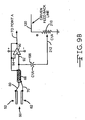
- Fig. 9B illustrates a basic form of the embodiment of Fig. 9A wherein the value of capacitor ClA may be varied electrically. While current measurement standards specify 20 pf. as the value for the capacitance seen by ion conducting surface 52, there may be situations where it is desired to change that value.
- Resistors 192 and 194 are replaced by a potentiometer 210 connected between the driven feedback line 120 and ground reference.
- the wiper arm 212 of potentiometer 210 is connected to the one terminal of capacitor C1A, the other terminal of which is operatively connected to ion conducting surface 52 as,in the embodiment of Fig. 9 .
- the adjustable range of potentiometer 210 from zero resistance to maximum resistance varies the value of capacitor ClA seen by surface 52 from zero to the actual value of ClA as indicated in the diagram.
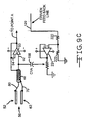
- Fig. 9C illustrates a preferred form of the embodiment of Fig. 9A for electrically varying the value of capacitor C1A.
- the series combination of resistors 220 and 222 is connected between driven feedback line 120 and ground reference.
- the junction of resistors 220, 222 is connected to the positive input of a buffer amplifier 224 similar to buffer amplifier 190 in the circuit of Fig. 9A .
- a potentiometer 226 is connected between the output of amplifier 224 and ground reference.
- the wiper arm 228 of potentiometer 226 is connected to the one terminal of capacitor ClA, the other terminal of which is operatively connected to ion conducting surface 52 as in the embodiment of Fig. 9A .
- buffer amplifier 224 prevents draining of the batteries in the circuit connected to driven feedback line 120.
- Potentiometer 226 varies the value of capacitor ClA. Typical values in an illustrative circuit would be 100K for resistor 220, 1M for resistor 222 and 10K for the maximum value of potentiometer 226. In an illustrative apparatus, the wiper arm of potentiometer 226 would be controlled by a manually operated knob provided with a dial showing the range of adjustable values of capacitor C1A.
- Potentiometer 226 can be replaced by a series combination of two resistors connected between the output of amplifier 224 and ground reference and with the junction of the two resistors connected to capacitor C1A.
- a digital to analog connector in combination with a microprocessor can be employed to change the ratio of the two resistors.
- potentiometer can be replaced by a digital potentiometer. In either event, the foregoing enables the value of capacitor ClA to be varied electrically by a computer operatively connected to the apparatus.
- Figs. 7 , 8 , and 9 can be easily combined as shown in the embodiment of Fig. 10 .
- the combination of the concepts of Figs. 7 , 8 , and 9 as shown in Fig. 10 provides a preferred embodiment.
- the resistance divider ratio as established by R5 and R6 in Fig. 7 when used in the embodiment of Fig. 10 can be reduced to a ratio of 1 to 1. This can be done because R5, shown connected to ground reference in Fig. 7 , is returned to the output of A4 in Fig. 10 .
- amplifier A4 has a resistance ratio connected to its input of 100 to 1, the A4 output has a 100 to 1 ratio which can be used directly by the A3 circuitry.
- indicator Vo can be a D.C. responding device or A.C. responding device, or preferable both.
- Indicator Vo may also be connected to point A instead of the driven feedback line 120 because the voltage range enhancement circuitry A2 and Q1 drives the driven feedback line 120 to match the signals at point (A).
- the value of Cl or ClA may be different values than those indicated to provide an ion collecting surface 52 capacitance which is different than the 200pf provided.
- the value of ClA may be varied electrically as previously described. Other variations may include the connection of the shield 68 to the driven feedback line 120 rather than to the output of amplifier/buffer (Al) because, here again, they are at the same signal level.
- a pair of series connected opposing zener diodes or other protective devices may be connected between the junction point of the cathode of diode D1, anode of diode D2 and the driven feedback line 120.
- the bandwidth of the monitor is not limited to a low frequency but extends to tens or hundreds of kilohertz depending on the components used, thus achieving high bandwidth capability, an objective of this invention.
- the ion collecting plate When the monitor of the present invention is used in the decay mode, the ion collecting plate is pre-charged to a voltage level above a predetermined start voltage for a decay timer. The time required for the incident air ion flow to discharge the ion collecting plate from the predetermined start voltage to a predetermined stop voltage is measured by the monitor.
- the monitor of the present invention When the monitor of the present invention is used in the float mode, the ion collecting plate initially is discharged to zero volts and then allowed to float to the voltage level dictated by incident air ion flow to the ion collecting plate.
- the monitor of the present invention has the capability of including a computer interface whereby a serial communications port and an applications software program enable the monitor to be operated from a computer.
- This advantageously allows for automation of data collection and data storage, accumulation of statistical information, graphic display of the plate voltage in the time domain, report generation, higher resolution of the decay time and the ability to adjust the start and stop voltage set points in one volt increments. Ion balance tests and decay tests can be performed and run in a series to automate repetitive tests and data collection, and data can be acquired and displayed in graphical form to greatly enhance the interpretation of test results.
- positive and negative decay tests can be performed to evaluate the ability of the ionizer to neutralize charges on surfaces in the work location.
- the decay waveform is observable and the decay time is given with ten millisecond resolution when the plate voltage reaches the programmed stop voltage.
- ion balance tests can be performed to evaluate the balance of positive and negative air ions.
- the test period can be of any specified length. The average, minimum and maximum plate voltages are recorded and displayed for each test period and the changes in plate voltage over time are graphed.
- Computer operation of the monitor also enables a series of tests to be programmed and run. It is often necessary to repeat the same series of balance and decay tests on a number of ionizers and to record the test results. It is highly advantageous to automate this by the computer capability of the monitor of the present invention.
- This is accomplished by entering a test sequence mode to program and execute a series of test steps. The procedure is begun by building a series of ion balance and decay test steps. For each step, one specifies the test type (balance or decay) and then is prompted by the program to specify the parameters for each test step.
- Programming and running a test series is further enhanced with provisions for looping and for programming time delays between test steps. Editing a series of tests is done by identifying the test step to be edited whereupon the program gives a prompt to enter new parameters for that step. Unwanted test steps are deleted using a similar method.
- Test data is saved as tab-delineated text files that are easily opened using spreadsheet software. One is able to record additional notes with the test data. From there, one can manipulate the data as needed for analysis. Test data also can be retrieved and displayed within the applications program.
Landscapes
- Physics & Mathematics (AREA)
- General Physics & Mathematics (AREA)
- Measurement Of Current Or Voltage (AREA)
Applications Claiming Priority (3)
| Application Number | Priority Date | Filing Date | Title |
|---|---|---|---|
| US13033199P | 1999-04-21 | 1999-04-21 | |
| US130331P | 1999-04-21 | ||
| PCT/US2000/010791 WO2000063707A1 (en) | 1999-04-21 | 2000-04-21 | Floating plate voltage monitor |
Publications (3)
| Publication Number | Publication Date |
|---|---|
| EP1192474A1 EP1192474A1 (en) | 2002-04-03 |
| EP1192474A4 EP1192474A4 (en) | 2006-08-09 |
| EP1192474B1 true EP1192474B1 (en) | 2012-05-23 |
Family
ID=22444187
Family Applications (1)
| Application Number | Title | Priority Date | Filing Date |
|---|---|---|---|
| EP00930129A Expired - Lifetime EP1192474B1 (en) | 1999-04-21 | 2000-04-21 | Floating plate voltage monitor |
Country Status (5)
| Country | Link |
|---|---|
| US (1) | US6433552B1 (enExample) |
| EP (1) | EP1192474B1 (enExample) |
| JP (1) | JP4990435B2 (enExample) |
| CN (1) | CN1184485C (enExample) |
| WO (1) | WO2000063707A1 (enExample) |
Families Citing this family (18)
| Publication number | Priority date | Publication date | Assignee | Title |
|---|---|---|---|---|
| US6985346B2 (en) * | 2003-01-29 | 2006-01-10 | Credence Technologies, Inc. | Method and device for controlling ionization |
| CN101437602B (zh) * | 2004-10-29 | 2011-04-06 | 特瑞克股份有限公司 | 离子平衡监视器 |
| US7439746B2 (en) * | 2006-10-27 | 2008-10-21 | Trek, Inc. | Electrostatic voltmeter |
| ES2338975B1 (es) * | 2008-11-12 | 2011-03-11 | Instituto De Tecnologia Electrica, Ite | Sensor de campo electrico. |
| CN104237620B (zh) * | 2009-04-30 | 2017-04-12 | 日置电机株式会社 | 电压检测装置 |
| CN101881791B (zh) * | 2009-04-30 | 2015-08-05 | 日置电机株式会社 | 电压检测装置 |
| JP2012103056A (ja) * | 2010-11-09 | 2012-05-31 | Hugle Electronics Inc | チャージプレートモニタ |
| JP5909785B2 (ja) * | 2010-12-07 | 2016-04-27 | デスコ インダストリーズ, インコーポレイテッド | イオン平衡測定及び調整のための遮蔽されたコンデンサ回路を有する電離平衡装置 |
| WO2013085952A1 (en) * | 2011-12-08 | 2013-06-13 | 3M Innovative Properties Company | An ionization monitoring device and method |
| CN104237605B (zh) * | 2014-09-04 | 2018-01-09 | 兰州空间技术物理研究所 | 一种高压静电电压测量装置 |
| CN104267064A (zh) * | 2014-09-04 | 2015-01-07 | 兰州空间技术物理研究所 | 一种用于航天器表面电位在轨监测的传感器 |
| JP6296965B2 (ja) * | 2014-11-28 | 2018-03-20 | 株式会社アドバンテスト | 電流測定回路および塩基配列解析装置 |
| CN105445526B (zh) * | 2015-11-20 | 2018-10-12 | 国家电网公司 | 一种运行条件下单芯电缆绝缘泄漏电流的测量结构 |
| FR3045160A1 (fr) * | 2015-12-09 | 2017-06-16 | Teqoya | Dispositif de mesure de charges electriques faibles, notamment ions. |
| CN105785246B (zh) * | 2016-04-25 | 2018-08-03 | 国网江苏省电力公司电力科学研究院 | 用于超高压电力电缆绝缘诊断的带电检测及在线监测装置 |
| CN206583996U (zh) * | 2016-11-25 | 2017-10-24 | 上海荣威塑胶工业有限公司 | 接地检测装置及水池系统 |
| US10548206B2 (en) * | 2017-09-05 | 2020-01-28 | International Business Machines Corporation | Automated static control |
| CN111404505B (zh) * | 2020-04-24 | 2023-05-26 | 北京卫星环境工程研究所 | 一种用于空间低能等离子体探测器的电压放大器装置 |
Family Cites Families (12)
| Publication number | Priority date | Publication date | Assignee | Title |
|---|---|---|---|---|
| US4370616A (en) * | 1980-08-15 | 1983-01-25 | Williams Bruce T | Low impedance electrostatic detector |
| US4433297A (en) * | 1981-06-22 | 1984-02-21 | Xerox Corporation | Time averaged amplitude comparison electrometer |
| US4835461A (en) * | 1984-04-13 | 1989-05-30 | Xerox Corporation | Microdeflector probe for electrostatic voltmeter |
| US4716371A (en) | 1985-07-22 | 1987-12-29 | The Simco Company, Inc. | Non-contact autoranging electrostatic fieldmeter with automatic distance indicator |
| US4928057A (en) * | 1986-10-28 | 1990-05-22 | Williams Bruce T | High speed D.C. non-contacting electrostatic voltage follower |
| US4740862A (en) * | 1986-12-16 | 1988-04-26 | Westward Electronics, Inc. | Ion imbalance monitoring device |
| US4809127A (en) * | 1987-08-11 | 1989-02-28 | Ion Systems, Inc. | Self-regulating air ionizing apparatus |
| US5016136A (en) * | 1989-02-17 | 1991-05-14 | Semtronics Corporation | Charge build-up and decay monitor |
| DE4231905C2 (de) * | 1992-09-18 | 1999-05-20 | Stiehl Hans Henrich Dr | Vorrichtung zur Messung von Ionen in einem Gas |
| JPH09280806A (ja) * | 1996-04-09 | 1997-10-31 | Nissan Motor Co Ltd | 静電容量式変位計 |
| US5886528A (en) * | 1996-09-10 | 1999-03-23 | Monroe Electronics, Inc. | Electrostatic voltage metering apparatus |
| US6130815A (en) * | 1997-11-10 | 2000-10-10 | Ion Systems, Inc. | Apparatus and method for monitoring of air ionization |
-
2000
- 2000-04-21 JP JP2000612761A patent/JP4990435B2/ja not_active Expired - Lifetime
- 2000-04-21 US US09/556,922 patent/US6433552B1/en not_active Expired - Lifetime
- 2000-04-21 CN CNB008092389A patent/CN1184485C/zh not_active Expired - Lifetime
- 2000-04-21 WO PCT/US2000/010791 patent/WO2000063707A1/en not_active Ceased
- 2000-04-21 EP EP00930129A patent/EP1192474B1/en not_active Expired - Lifetime
Also Published As
| Publication number | Publication date |
|---|---|
| JP2003508725A (ja) | 2003-03-04 |
| EP1192474A4 (en) | 2006-08-09 |
| US6433552B1 (en) | 2002-08-13 |
| WO2000063707A1 (en) | 2000-10-26 |
| CN1375061A (zh) | 2002-10-16 |
| HK1050566A1 (en) | 2003-06-27 |
| EP1192474A1 (en) | 2002-04-03 |
| JP4990435B2 (ja) | 2012-08-01 |
| WO2000063707A9 (en) | 2002-06-06 |
| CN1184485C (zh) | 2005-01-12 |
Similar Documents
| Publication | Publication Date | Title |
|---|---|---|
| EP1192474B1 (en) | Floating plate voltage monitor | |
| Collins | Measurement of charge distribution in electrets | |
| US4370616A (en) | Low impedance electrostatic detector | |
| Secker | The desing of simple instruments for measurement of charge on insulating surfaces | |
| US3866114A (en) | Electrostatic measurement system | |
| WO2008052177A2 (en) | Electrostatic voltmeter | |
| KR100329359B1 (ko) | 미소용량측정 시스템 및 프로빙 시스템 | |
| CA1113580A (en) | Displacement current sensor | |
| US7427864B2 (en) | Ion balance monitor | |
| Kumar et al. | Capacitive sensor for the measurement of VFTO in GIS | |
| JP2607858Y2 (ja) | 静電容量形音響トランスデューサを試験するためのシステム | |
| US4673885A (en) | Devices for reading the quantities of electrical charges borne by a dielectric | |
| Vosteen | A review of current electrostatic measurement techniques and their limitations | |
| Brodie et al. | Measurement of charge transfer in electrographic processes | |
| CN114965660A (zh) | 一种介质材料静电衰减时间一体化测试装置 | |
| US5016136A (en) | Charge build-up and decay monitor | |
| Chubb et al. | Comparative studies on methods of charge decay measurement | |
| HK1050566B (en) | Floating plate voltage monitor | |
| KR20000071474A (ko) | 전극 배열을 위한 시험 장치 및 관련된 방법 | |
| Horenstein et al. | Measurement of electrostatic fields, voltages, and charges | |
| SU1744656A1 (ru) | Бесконтактный датчик поверхностных зар дов и потенциалов | |
| Mazo et al. | A low cost current follower for voltammetric measurements with ultramicroelectrodes | |
| JP3196974B2 (ja) | 検電器 | |
| SU1144059A1 (ru) | Способ определени удельной проводимости высокоомных микрообразцов | |
| Ehrmaier et al. | Some results in measuring static decay |
Legal Events
| Date | Code | Title | Description |
|---|---|---|---|
| PUAI | Public reference made under article 153(3) epc to a published international application that has entered the european phase |
Free format text: ORIGINAL CODE: 0009012 |
|
| 17P | Request for examination filed |
Effective date: 20011121 |
|
| AK | Designated contracting states |
Kind code of ref document: A1 Designated state(s): AT BE CH CY DE DK ES FI FR GB GR IE IT LI LU MC NL PT SE |
|
| A4 | Supplementary search report drawn up and despatched |
Effective date: 20060711 |
|
| 17Q | First examination report despatched |
Effective date: 20071228 |
|
| REG | Reference to a national code |
Ref country code: DE Ref legal event code: R079 Ref document number: 60047196 Country of ref document: DE Free format text: PREVIOUS MAIN CLASS: G01R0019000000 Ipc: G01R0029240000 |
|
| GRAP | Despatch of communication of intention to grant a patent |
Free format text: ORIGINAL CODE: EPIDOSNIGR1 |
|
| RIC1 | Information provided on ipc code assigned before grant |
Ipc: G01R 29/24 20060101AFI20111028BHEP |
|
| GRAS | Grant fee paid |
Free format text: ORIGINAL CODE: EPIDOSNIGR3 |
|
| GRAA | (expected) grant |
Free format text: ORIGINAL CODE: 0009210 |
|
| RIN1 | Information on inventor provided before grant (corrected) |
Inventor name: WILLIAMS, BRUCE |
|
| AK | Designated contracting states |
Kind code of ref document: B1 Designated state(s): AT BE CH CY DE DK ES FI FR GB GR IE IT LI LU MC NL PT SE |
|
| REG | Reference to a national code |
Ref country code: GB Ref legal event code: FG4D |
|
| REG | Reference to a national code |
Ref country code: DE Ref legal event code: R082 Ref document number: 60047196 Country of ref document: DE Representative=s name: PATENTANWAELTE FREISCHEM, DE Ref country code: CH Ref legal event code: EP Ref country code: DE Ref legal event code: R082 Ref document number: 60047196 Country of ref document: DE Representative=s name: FREISCHEM & PARTNER PATENTANWAELTE MBB, DE |
|
| REG | Reference to a national code |
Ref country code: AT Ref legal event code: REF Ref document number: 559316 Country of ref document: AT Kind code of ref document: T Effective date: 20120615 |
|
| REG | Reference to a national code |
Ref country code: IE Ref legal event code: FG4D |
|
| REG | Reference to a national code |
Ref country code: NL Ref legal event code: T3 |
|
| REG | Reference to a national code |
Ref country code: DE Ref legal event code: R096 Ref document number: 60047196 Country of ref document: DE Effective date: 20120726 |
|
| PG25 | Lapsed in a contracting state [announced via postgrant information from national office to epo] |
Ref country code: SE Free format text: LAPSE BECAUSE OF FAILURE TO SUBMIT A TRANSLATION OF THE DESCRIPTION OR TO PAY THE FEE WITHIN THE PRESCRIBED TIME-LIMIT Effective date: 20120523 Ref country code: CY Free format text: LAPSE BECAUSE OF FAILURE TO SUBMIT A TRANSLATION OF THE DESCRIPTION OR TO PAY THE FEE WITHIN THE PRESCRIBED TIME-LIMIT Effective date: 20120523 Ref country code: FI Free format text: LAPSE BECAUSE OF FAILURE TO SUBMIT A TRANSLATION OF THE DESCRIPTION OR TO PAY THE FEE WITHIN THE PRESCRIBED TIME-LIMIT Effective date: 20120523 |
|
| REG | Reference to a national code |
Ref country code: AT Ref legal event code: MK05 Ref document number: 559316 Country of ref document: AT Kind code of ref document: T Effective date: 20120523 |
|
| PG25 | Lapsed in a contracting state [announced via postgrant information from national office to epo] |
Ref country code: PT Free format text: LAPSE BECAUSE OF FAILURE TO SUBMIT A TRANSLATION OF THE DESCRIPTION OR TO PAY THE FEE WITHIN THE PRESCRIBED TIME-LIMIT Effective date: 20120924 Ref country code: GR Free format text: LAPSE BECAUSE OF FAILURE TO SUBMIT A TRANSLATION OF THE DESCRIPTION OR TO PAY THE FEE WITHIN THE PRESCRIBED TIME-LIMIT Effective date: 20120824 |
|
| PG25 | Lapsed in a contracting state [announced via postgrant information from national office to epo] |
Ref country code: BE Free format text: LAPSE BECAUSE OF FAILURE TO SUBMIT A TRANSLATION OF THE DESCRIPTION OR TO PAY THE FEE WITHIN THE PRESCRIBED TIME-LIMIT Effective date: 20120523 |
|
| PG25 | Lapsed in a contracting state [announced via postgrant information from national office to epo] |
Ref country code: DK Free format text: LAPSE BECAUSE OF FAILURE TO SUBMIT A TRANSLATION OF THE DESCRIPTION OR TO PAY THE FEE WITHIN THE PRESCRIBED TIME-LIMIT Effective date: 20120523 Ref country code: AT Free format text: LAPSE BECAUSE OF FAILURE TO SUBMIT A TRANSLATION OF THE DESCRIPTION OR TO PAY THE FEE WITHIN THE PRESCRIBED TIME-LIMIT Effective date: 20120523 |
|
| PG25 | Lapsed in a contracting state [announced via postgrant information from national office to epo] |
Ref country code: IT Free format text: LAPSE BECAUSE OF FAILURE TO SUBMIT A TRANSLATION OF THE DESCRIPTION OR TO PAY THE FEE WITHIN THE PRESCRIBED TIME-LIMIT Effective date: 20120523 |
|
| PLBE | No opposition filed within time limit |
Free format text: ORIGINAL CODE: 0009261 |
|
| STAA | Information on the status of an ep patent application or granted ep patent |
Free format text: STATUS: NO OPPOSITION FILED WITHIN TIME LIMIT |
|
| PG25 | Lapsed in a contracting state [announced via postgrant information from national office to epo] |
Ref country code: ES Free format text: LAPSE BECAUSE OF FAILURE TO SUBMIT A TRANSLATION OF THE DESCRIPTION OR TO PAY THE FEE WITHIN THE PRESCRIBED TIME-LIMIT Effective date: 20120903 |
|
| 26N | No opposition filed |
Effective date: 20130226 |
|
| REG | Reference to a national code |
Ref country code: DE Ref legal event code: R097 Ref document number: 60047196 Country of ref document: DE Effective date: 20130226 |
|
| PG25 | Lapsed in a contracting state [announced via postgrant information from national office to epo] |
Ref country code: MC Free format text: LAPSE BECAUSE OF FAILURE TO SUBMIT A TRANSLATION OF THE DESCRIPTION OR TO PAY THE FEE WITHIN THE PRESCRIBED TIME-LIMIT Effective date: 20120523 |
|
| REG | Reference to a national code |
Ref country code: CH Ref legal event code: PL |
|
| REG | Reference to a national code |
Ref country code: IE Ref legal event code: MM4A |
|
| PG25 | Lapsed in a contracting state [announced via postgrant information from national office to epo] |
Ref country code: CH Free format text: LAPSE BECAUSE OF NON-PAYMENT OF DUE FEES Effective date: 20130430 Ref country code: LI Free format text: LAPSE BECAUSE OF NON-PAYMENT OF DUE FEES Effective date: 20130430 |
|
| PG25 | Lapsed in a contracting state [announced via postgrant information from national office to epo] |
Ref country code: IE Free format text: LAPSE BECAUSE OF NON-PAYMENT OF DUE FEES Effective date: 20130421 |
|
| PG25 | Lapsed in a contracting state [announced via postgrant information from national office to epo] |
Ref country code: LU Free format text: LAPSE BECAUSE OF NON-PAYMENT OF DUE FEES Effective date: 20130421 |
|
| REG | Reference to a national code |
Ref country code: FR Ref legal event code: PLFP Year of fee payment: 17 |
|
| REG | Reference to a national code |
Ref country code: FR Ref legal event code: PLFP Year of fee payment: 18 |
|
| REG | Reference to a national code |
Ref country code: FR Ref legal event code: PLFP Year of fee payment: 19 |
|
| PGFP | Annual fee paid to national office [announced via postgrant information from national office to epo] |
Ref country code: NL Payment date: 20180410 Year of fee payment: 19 |
|
| PGFP | Annual fee paid to national office [announced via postgrant information from national office to epo] |
Ref country code: DE Payment date: 20180625 Year of fee payment: 19 |
|
| PGFP | Annual fee paid to national office [announced via postgrant information from national office to epo] |
Ref country code: GB Payment date: 20180426 Year of fee payment: 19 |
|
| PGFP | Annual fee paid to national office [announced via postgrant information from national office to epo] |
Ref country code: FR Payment date: 20190313 Year of fee payment: 20 |
|
| REG | Reference to a national code |
Ref country code: DE Ref legal event code: R119 Ref document number: 60047196 Country of ref document: DE |
|
| REG | Reference to a national code |
Ref country code: NL Ref legal event code: MM Effective date: 20190501 |
|
| GBPC | Gb: european patent ceased through non-payment of renewal fee |
Effective date: 20190421 |
|
| PG25 | Lapsed in a contracting state [announced via postgrant information from national office to epo] |
Ref country code: DE Free format text: LAPSE BECAUSE OF NON-PAYMENT OF DUE FEES Effective date: 20191101 Ref country code: NL Free format text: LAPSE BECAUSE OF NON-PAYMENT OF DUE FEES Effective date: 20190501 Ref country code: GB Free format text: LAPSE BECAUSE OF NON-PAYMENT OF DUE FEES Effective date: 20190421 |