EP1190322B1 - Semiconductor parallel tester - Google Patents
Semiconductor parallel tester Download PDFInfo
- Publication number
- EP1190322B1 EP1190322B1 EP00944961A EP00944961A EP1190322B1 EP 1190322 B1 EP1190322 B1 EP 1190322B1 EP 00944961 A EP00944961 A EP 00944961A EP 00944961 A EP00944961 A EP 00944961A EP 1190322 B1 EP1190322 B1 EP 1190322B1
- Authority
- EP
- European Patent Office
- Prior art keywords
- pogo
- tester
- pin
- assembly
- semiconductor
- Prior art date
- Legal status (The legal status is an assumption and is not a legal conclusion. Google has not performed a legal analysis and makes no representation as to the accuracy of the status listed.)
- Expired - Lifetime
Links
Images



Classifications
-
- G—PHYSICS
- G01—MEASURING; TESTING
- G01R—MEASURING ELECTRIC VARIABLES; MEASURING MAGNETIC VARIABLES
- G01R31/00—Arrangements for testing electric properties; Arrangements for locating electric faults; Arrangements for electrical testing characterised by what is being tested not provided for elsewhere
- G01R31/28—Testing of electronic circuits, e.g. by signal tracer
- G01R31/317—Testing of digital circuits
- G01R31/3181—Functional testing
- G01R31/319—Tester hardware, i.e. output processing circuits
- G01R31/31903—Tester hardware, i.e. output processing circuits tester configuration
- G01R31/31905—Interface with the device under test [DUT], e.g. arrangements between the test head and the DUT, mechanical aspects, fixture
-
- G—PHYSICS
- G01—MEASURING; TESTING
- G01R—MEASURING ELECTRIC VARIABLES; MEASURING MAGNETIC VARIABLES
- G01R31/00—Arrangements for testing electric properties; Arrangements for locating electric faults; Arrangements for electrical testing characterised by what is being tested not provided for elsewhere
- G01R31/28—Testing of electronic circuits, e.g. by signal tracer
- G01R31/2851—Testing of integrated circuits [IC]
-
- G—PHYSICS
- G01—MEASURING; TESTING
- G01R—MEASURING ELECTRIC VARIABLES; MEASURING MAGNETIC VARIABLES
- G01R31/00—Arrangements for testing electric properties; Arrangements for locating electric faults; Arrangements for electrical testing characterised by what is being tested not provided for elsewhere
- G01R31/28—Testing of electronic circuits, e.g. by signal tracer
- G01R31/2851—Testing of integrated circuits [IC]
- G01R31/2886—Features relating to contacting the IC under test, e.g. probe heads; chucks
- G01R31/2889—Interfaces, e.g. between probe and tester
Definitions
- the invention relates generally to automatic test equipment for testing semiconductor devices, and more particularly a semiconductor tester capable of simultaneously testing a relatively large number of semiconductor devices in parallel.
- One of the more critical processes involves electronically testing each and every chip according to predetermined criteria. This generally involves stimulating the inputs of the device to generate expected output signals, and monitoring the actual output signals to verify that the actual and expected outputs match. The test procedure is often conducted first at the wafer level to weed out devices early in the production process, and later at the packaged-device level.
- ATE automatic test equipment
- testers To carry out the test process, semiconductor manufacturers typically utilize sophisticated machines commonly referred to as automatic test equipment (ATE) or testers. ATE designed for a production environment is often fairly costly, thereby contributing to the overall unit cost for each semiconductor device. Semiconductor manufacturers have thus realized that in order to minimize device unit costs, and remain competitive, the ATE must provide significant cost savings to warrant its high cost.
- ATE One way that ATE contributes to lower fabrication costs is by simultaneously testing groups of devices-under-test (DUTs) in parallel. This is commonly done for relatively low pin count memory devices and dramatically improves device throughput. This consequently reduces unit costs.
- Conventional parallel testers typically include a computer-driven test controller or mainframe unit that couples to a separately disposed testhead via a fairly large cable bundle. The bundle includes several hundred signal cables that collectively terminate in a first backplane assembly.
- the testhead generally includes a plurality of circuit boards that mount the pin electronics necessary to electronically interface with the pins of each DUT. Connections from the pin electronics are routed to a second backplane assembly, and carried through to individual double-sided pogo pins installed in a pogo or probe ring.
- the second backplane assembly is often constructed with relatively long trace patterns that tend to require sophisticated and expensive impedance control schemes in an effort to optimize signal quality. Interface schemes similar to that described above are disclosed in U.S. Patents Nos. 5,546,405 to Golla, and 5,907,245 to Fredrickson.
- the dimensions of the probe ring is generally dependent on the size of a semiconductor wafer and the probe card that engages the wafer.
- Semiconductor wafers are often around 200 mm in diameter that dictates a 300-350 mm diameter probe card for signal routing purposes.
- the wafer in turn, collectively comprises tens of DUTs having contact points accessible by finely tipped probes.
- Each signal path through the tester corresponding to a DUT contact point or "pin" must generally comprise a 50 ohm transmission line for optimal signal quality. This often involves surrounding each probe ring signal path with ground paths.
- MTBF mean time before failure
- MTTR mean time to repair
- afects unit costs in much the same way as the MTBF.
- the signal path connections are often routed through various areas in the cable bundle, the respective backplane assemblies, and the pogo ring with little regard for quick troubleshooting and repair or replacement. This often results in a relatively long MTTR for a tester should a problem arise in one of the connections.
- the semiconductor parallel tester of the present invention provides the capability of simultaneously testing groups of DUTs without compromising on the signal integrity for each tester signal path.
- the tester also substantially improves the mean time between failures by minimizing the complexity of the signal interconnections. Further, the mean time to repair is dramatically minimized by modularizing many of the tester components.
- the invention in one form comprises a semiconductor tester for testing a plurality of DUTs secured to a handling apparatus, said tester includes a system controller for initiating system test signals, and a pin electronics assembly responsive to said system test signals for generating test pattern signals for application to said plurality of DUTs, said semiconductor tester characterized by a signal interface adapted for defining a plurality of direct signal paths, when said tester is coupled to said handling apparatus, between said handling apparatus and said pin electronics assembly, wherein said signal interface includes, a substantially circular probe ring formed with a plurality of axially opening cavities, said cavities disposed in a spaced-apart annular configuration; and a plurality of modular harness assemblies, each of said plurality of modular harness assemblies including respective proximal and distal ends, said proximal end including a pogo module for nesting in one of said plurality of axially opening cavities and said distal end including at least one connector for engaging said pin electronics assembly, said pogo module formed with an array of closely spaced throughbores,
- the pogo pin assembly for high-density integration in a semiconductor tester prober interface, includes a coaxial cable having a center conductor and a shield.
- the shield terminates at a distal end with the center conductor projecting axially from the distal end and defining a distal tip.
- a pogo pin is fixed in close-spaced axial relationship to the distal tip via a pogo receptacle.
- An impedance compensation element couples to the cable and pogo pin.
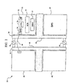
- a semiconductor tester according to one embodiment of the present invention, and generally designated 10, includes a system controller 12 and pin electronics 20 responsive to the system controller to generate test signals for application to a plurality of devices-under-test (DUTs) 16 disposed in a handling apparatus 140.
- a signal interface 150 defines a plurality of direct signal paths to couple the pin electronics to the handling apparatus, thereby maximizing the density of a plurality of signal paths, minimizing the number of connections for each signal path, and correspondingly improving tester reliability.
- the tester 10 including the system controller 12 and the associated pin electronics 20, is housed in a self-supporting frame (not shown) defining an integrated test cell.
- the integrated test cell frame minimizes clean-room floorspace with a relatively small footprint.
- the system controller 12 preferably comprises a Windows NT platform-based computer including, for example, a Pentium class processor running at several hundred MHz. Peripherals such as a 4GB hard drive memory, 64 MB of RAM memory, and a SVGA controller/monitor round out the computer.
- local processors 56 Figure 2 are disposed in the pin electronics 20 as more fully explained below to provide asynchronous test control capabilities between DUTs 16. This substantially improves tester throughput because of the unique and somewhat unpredictable electrical characteristics of flash memory devices.
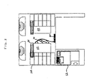
- the pin electronics 20 ( Figure 1) comprises a plurality of modularized board assemblies 30 mounted in a pair of oppositely disposed card cages 24 and 26 ( Figure 3).
- each card cage preferably includes five DC power modules 28 ( Figure 3), a power controller module (not shown), a calibration board (not shown), and one backplane assembly 29.
- the backplane assembly differs somewhat from a conventional backplane assembly in that relatively short signal traces (not shown) are employed to minimize any undesirable impedance problems.
- each channel board assembly 30 includes a rigid metallic board frame split into respective members 32 and 34.
- the frame members are formed respectively with T-shaped borders that sandwich the edges of the respective channel cards 40 and 42.
- a pair of hinges 44 and 46 defining a hinge assembly join the rear edges 48 and 50 of both frame members to form a spine.
- the hinge assembly allows the frame members, when plugged into the backplane assembly 29, to fold in a substantially 180 degree open relationship. Fully assembled, the preferred board frame assembly dimensions are approximately 20 X 20 inches.
- the two channel cards 40 and 42 in the channel board assembly 30 preferably comprise respective copies of a thirty-two channel channel card (for a total of sixty-four channels).
- Each channel card is formed similar to those employed in the Teradyne Model J750 Integra tester, manufactured by Teradyne, Inc., Boston, Mass.
- a precision force/measuring instrument (PMU) mounts to the channel cards.
- the third board 52 Disposed opposite the channel cards 40 and 42 in each board assembly 30 is a third board 52.
- the third board preferably comprises a memory test module assembly configured with an arithmetic pattern generator (APG) 54 and a station controller or local processor 56 for asynchronous control of a particular DUT with respect to the other simultaneously tested DUTs 16.
- APG arithmetic pattern generator
- SBA error catch ram
- DBM data buffer memory
- DUT power supply (DPS) 59 modules are mounted on the board assembly 30.
- the channel cards 40 and 42 and the memory test module 52 are interconnected with a series of flexible ribbon cables 58, and additionally coupled to the backplane assembly 29 ( Figure 1).
- each board frame assembly substantially includes sufficient tester resources necessary to test one DUT 16. Consequently, to test thirty-two DUTs in parallel, a total of thirty-two board frame assemblies are implemented in the two card cages 24 and 26.
- the calibration board plugs into the backplane assembly 29 for each card cage 24 adjacent the channel board assemblies 30 and includes a system crystal clock (not shown), and a loadboard ID communications device (not shown).
- a plurality of timing calibration master driver/compare circuits are also provided.
- the ability to minimize the backplane assembly trace paths arises from the implementation of a plurality of modular harness assemblies 70 that route the signal paths from the pin electronics 20 to a probe ring 60. This also provides a compact mechanism for distributing tester signals in an organized manner.
- the probe ring and the harness assemblies collectively comprise the signal interface 150 ( Figure 1).
- the probe ring 60 comprises a substantially circular-shaped aluminum casting including a radially projecting peripheral flange 62.
- a plurality of open-ended cavities 64 are formed in an annular configuration in the ring for nesting respective pogo modules 80 ( Figure 6).
- Two additional reduced-in-size cavities 66 are formed on opposite sides of the probe ring for receiving respective calibration modules (not shown).
- the casting is formed approximately fourteen inches in diameter and three inches thick, with a total of ten formed cavities.
- a centrally disposed rectangular opening 68 is formed in the ring to provide clearance for a pivot connection to a self-alignment mechanism (not shown). A more detailed description of the self-alignment mechanism is found in previously referenced copending U.S. Patent Application Serial Number 09/410857, entitled "Integrated Test Cell.”
- each harness assembly includes a cable bundle 65 of signal and power supply cables that collectively terminate proximally at a pogo module 80.
- the bundle includes a plurality of branches 69, 71, 73, 75 and 77 that include respective HDM connectors 81, 83, 85, 87, and 89 for coupling to respective first through fourth board frame assemblies 72, 74, 76, 78 ( Figure 1) and a DUT power supply board (not shown).
- Each harness conveniently supports the testing of four DUTs, and is easily serviceable and replaceable.
- the pogo module 80 comprises an aluminum housing formed with an upper mounting flange 84 that projects outwardly from a polygonal wall 86.
- the wall is formed integral with and surrounds a cylindrical engagement interface 88 having a high-density array of closely-spaced throughbores 90.
- the throughbores are configured to receive approximately ninety signal pogo pin assemblies 110 having respective signal pogo pins 130.
- Interposed between the throughbores is a high-density array of downwardly opening blind bores 92 for receiving ground pogo pins 94.
- Each signal pogo pin is substantially surrounded by a group of the ground pogo pins to maintain a substantially ideal fifty ohm transmission line environment for optimal signal quality.
- a polygonal pogo pin protector 96 Disposed concentrically around the engagement surface 88 of the pogo module 80 is a polygonal pogo pin protector 96 formed with a plurality of seats 98.
- the seats are constructed to align opposite similarly formed bores 102 disposed in the polygonal wall 86, and cooperate therewith to house respective springs 106.
- a self-aligning snap retainer (not shown) secures the pogo pin protector to the pogo module 80.
- the calibration modules are formed substantially similar to the pogo modules 80 but in reduced dimensions commensurate with the reduced number of connections required between the calibration boards (not shown) and the probe ring 60.
- each signal pogo pin assembly 110 includes a high fidelity RG-type coaxial cable including a shield conductor 112 and a center conductor 114. Each cable is approximately 37 inches long for bundling in a harness assembly 70 as previously described above.
- the center conductor of each cable terminates in the crimped portion 117 of a metallic pogo receptacle 118 available from Rika Denshi of Tokyo, Japan.
- the crimped termination between the center conductor and the pogo pin creates a gas-tight cavity 119.
- One of the more significant features of the present invention involves the use of an insulator assembly 120 that substantially surrounds the center conductor 114 and the crimped portion 117 to compensate for any impedance mismatching caused by pogo component junctions, terminations and the like. Compensating for any adverse effects to the fifty ohm transmission line impedance is especially important to ensure the optimal signal quality for each signal path through the densely packed probe ring.
- the insulator assembly 120 includes a first cylindrical insulator 122 formed to entirely surround a portion of the center conductor 114 and abut a ground ferrule 124, the ground ferrule is soldered to the shield and snugly fits within a throughbore 90 to establish a ground path between the shield and the pogo module 80.
- a second insulator 126 is disposed adjacent the first insulator, and is formed with a C-shaped configuration and a distal taper 128 to complementally engage the crimped portion 117 of the pogo receptacle 118.
- a signal pogo pin 130 available also from Rika Denshi, nests within the pogo receptacle and includes a retractable tip 132 for contacting a probe card contact (not shown).
- the probe card ranges from between 300 to 350 mm in diameter to support 2048 signal channels and includes contacts (not shown) that couple to the pins of from one to thirty-two DUTs, providing a relatively high level of parallelism to maximize tester throughput.
- a preferred prober is the TEL Model P8XL prober, manufactured by Tokyo Electron Ltd. of Tokyo, Japan.
- the handling apparatus 140 comprises a handler (not shown), such as the Galileo Model handler, available from Kinetrix, Inc. of Bedford, New Hampshire.
- handlers provide the capability of testing packaged-devices mounted on loadboards (not shown) that interface with the probe ring.
- the semiconductor manufacturer installs a semiconductor wafer (not shown) formed with up to several hundred devices into the prober 140, and secures the probecard 134 thereover.
- the probecard generally includes an engagement mechanism that contacts the individual "pins" of each device to enable subsequent coupling to the probe ring 60 via the signal and ground pogo pins 130 and 94.
- One of the unique features of the preferred prober involves a quick change mechanism (not shown) that provides for swapping of wafers or probe cards without the need for undocking the prober 140 from the tester 10.
- the prober and tester collectively define a test system 200.
- the tester 10 system controller 12 provides a convenient operator interface for a user to monitor the progress and results of the parallel tests.
- each DUT 16 is subjected to a plurality of tests that verify the functional operation of the device according to manufacturing specifications. To provide clarity in the operation of the test system, the following description addresses the signal routing during test for a single DUT.
- the test generally involves the generation of pattern signals by each APG 54 according to software carried out by each local processor 56.
- the signals are distributed by the channel cards 40 and 42 and define individual channels or signal paths corresponding to separate pins of the DUT. Signals propagating along channels associated with a single device are routed from the channel cards to the backplane assembly 29, and thereupon transferred through a corresponding HDM connector to the separate coax cables that comprise a branch portion of one harness assembly 70.
- the signals reach the high density pogo module 80 and propagate along the center conductor/pogo pin connection, a slight degradation to the fifty-ohm transmission line impedance occurs at the proximal tip of the ground ferrule 90. The degradation is immediately compensated by an inverse effect generated by the insulator assembly 120.
- the crimped portion 117 of the pogo receptacle causes an additional impedance mismatch that is conveniently compensated for by the effects of the C-shaped second insulator 126.
- the propagating signals then conduct along the respective signal pogo pins, with a relatively high quality pulse-shape made possible by the surrounding ground pogo pins 94 around each signal path.
- the signals are then routed along the probe card 134, and translated along fine electrical probes (not shown) that engage the semiconductor wafer (not shown), and the particular DUT 16 of interest.
- the signals may be written to specific addresses within the DUT, and subsequently read back for comparison to expected values.
- MTBF mean-time-between-failures
- the modular construction of the present invention provides a quick troubleshooting capability to locate entire signal paths, reducing the time required in isolating a potential problem. Even more importantly, the modularity of the invention allows an efficient and straightforward replacement of a channel board assembly 30, or a harness assembly 70, or even a pogo pin assembly 110 with minimal effort and stand down time. This dramatically minimizes the "mean-time-for-repair (MTFR) parameter for the tester which also substantially contributes to overall lower semiconductor production costs.
- MTFR mean-time-for-repair
- the signal interface of the present invention provides a way of carrying out fairly large-scale parallel testing on conventionally sized wafers or loadboards without sacrificing signal integrity through the probe ring. This is accomplished through the implementation of the unique pogo pin assembly that provides impedance compensation for any transmission line degradations.
- DUTs having relatively small pin counts may be tested by combining more than one sixty-four channel board.
- the parallelism aspect of the present invention has been described with reference primarily to wafer-level probe testing, the invention is applicable also to packaged-level devices manipulated by a handler, and interfaced through a loadboard rather than a probecard. Consequently, for purposes of the invention, the term handling apparatus is used broadly to denote either the use of a handler or a prober.
Landscapes
- Engineering & Computer Science (AREA)
- General Engineering & Computer Science (AREA)
- Physics & Mathematics (AREA)
- General Physics & Mathematics (AREA)
- Computer Hardware Design (AREA)
- Microelectronics & Electronic Packaging (AREA)
- Tests Of Electronic Circuits (AREA)
- Testing Or Measuring Of Semiconductors Or The Like (AREA)
- Test And Diagnosis Of Digital Computers (AREA)
- Measuring Leads Or Probes (AREA)
Description
Claims (6)
- A semiconductor tester (10) for testing a plurality of DUTs (16) secured to a handling apparatus (140), said tester includes a system controller (12) for initiating system test signals, and a pin electronics assembly (20) responsive to said system test signals for generating test pattern signals for application to said plurality of DUTs, said semiconductor tester characterized by:a signal interface (150) adapted for defining a plurality of direct signal paths (70), when said tester is coupled to said handling apparatus, between said handling apparatus and said pin electronics assembly, wherein said signal interface includes,a substantially circular probe ring (60) formed with a plurality of axially opening cavities (64), said cavities disposed in a spaced-apart annular configuration; anda plurality of modular harness assemblies (70), each of said plurality of modular harness assemblies including respective proximal and distal ends, said proximal end including a pogo module (80) for nesting in one of said plurality of axially opening cavities and said distal end including at least one connector (81-89) for engaging said pin electronics assembly, said pogo module formed with an array of closely spaced throughbores (90), each of said throughbores configured to receive a pogo pin assembly (110).
- A semiconductor tester (10) according to claim 1 wherein said probe ring (60) is formed of a casting and includes a radially projecting peripheral flange (62), said probe ring further including a centrally formed and open-ended slot (68) for receiving a pivot arm.
- A semiconductor tester (10) according to claim 1 wherein:said pogo module (80) comprises an aluminum housing.
- A semiconductor tester (10) according to claim 1, wherein:said pogo module (80) includes a retractable spring-loaded pogo pin protector (96).
- A semiconductor tester (10) according to claim 1 wherein:each of said plurality of modular harness assemblies (70) includes a cable bundle strain relief.
- A semiconductor tester (10) according to claim 1 wherein said pogo pin assembly (110) includes:a coaxial cable having a center conductor (114) and a shield (112), said shield terminating at a distal end, and said center conductor projecting axially from said distal end and defining a distal tip;a pogo pin (130) fixed in close-spaced axial relationship to said distal tip via a pogo receptacle (118); andan impedance compensation element (120) coupled to said cable and pogo pin.
Applications Claiming Priority (3)
| Application Number | Priority Date | Filing Date | Title |
|---|---|---|---|
| US09/340,832 US6476628B1 (en) | 1999-06-28 | 1999-06-28 | Semiconductor parallel tester |
| US340832 | 1999-06-28 | ||
| PCT/US2000/017792 WO2001001247A2 (en) | 1999-06-28 | 2000-06-28 | Semiconductor parallel tester |
Publications (2)
| Publication Number | Publication Date |
|---|---|
| EP1190322A2 EP1190322A2 (en) | 2002-03-27 |
| EP1190322B1 true EP1190322B1 (en) | 2003-06-11 |
Family
ID=23335115
Family Applications (1)
| Application Number | Title | Priority Date | Filing Date |
|---|---|---|---|
| EP00944961A Expired - Lifetime EP1190322B1 (en) | 1999-06-28 | 2000-06-28 | Semiconductor parallel tester |
Country Status (8)
| Country | Link |
|---|---|
| US (1) | US6476628B1 (en) |
| EP (1) | EP1190322B1 (en) |
| JP (1) | JP5173097B2 (en) |
| KR (1) | KR100696321B1 (en) |
| DE (1) | DE60003312T2 (en) |
| MY (1) | MY119234A (en) |
| TW (1) | TW469485B (en) |
| WO (1) | WO2001001247A2 (en) |
Families Citing this family (37)
| Publication number | Priority date | Publication date | Assignee | Title |
|---|---|---|---|---|
| US6671844B1 (en) * | 2000-10-02 | 2003-12-30 | Agilent Technologies, Inc. | Memory tester tests multiple DUT's per test site |
| US6988232B2 (en) * | 2001-07-05 | 2006-01-17 | Intellitech Corporation | Method and apparatus for optimized parallel testing and access of electronic circuits |
| US7009381B2 (en) * | 2002-03-21 | 2006-03-07 | Agilent Technologies, Inc. | Adapter method and apparatus for interfacing a tester with a device under test |
| JP3621938B2 (en) * | 2002-08-09 | 2005-02-23 | 日本電子材料株式会社 | Probe card |
| US6842022B2 (en) * | 2002-09-20 | 2005-01-11 | Agilent Technologies, Inc. | System and method for heterogeneous multi-site testing |
| US7437261B2 (en) * | 2003-02-14 | 2008-10-14 | Advantest Corporation | Method and apparatus for testing integrated circuits |
| KR20060019552A (en) * | 2003-05-22 | 2006-03-03 | 테세다 코포레이션 | Tester Structure for Semiconductor Integrated Circuit Test |
| US7053648B2 (en) * | 2003-06-09 | 2006-05-30 | Credence Systems Corporation | Distributed, load sharing power supply system for IC tester |
| KR100498509B1 (en) * | 2003-11-12 | 2005-07-01 | 삼성전자주식회사 | Flash memory test system capable of test time reduction and electrical test Method thereof |
| US7464287B2 (en) * | 2004-03-31 | 2008-12-09 | Intel Corporation | Strategy to verify asynchronous links across chips |
| US7913002B2 (en) * | 2004-08-20 | 2011-03-22 | Advantest Corporation | Test apparatus, configuration method, and device interface |
| US7543200B2 (en) * | 2005-02-17 | 2009-06-02 | Advantest Corporation | Method and system for scheduling tests in a parallel test system |
| US20060214679A1 (en) * | 2005-03-28 | 2006-09-28 | Formfactor, Inc. | Active diagnostic interface for wafer probe applications |
| US7292059B2 (en) * | 2005-03-31 | 2007-11-06 | Credence Systems Corporation | Power supply assembly for a semiconductor circuit tester |
| JP2006343146A (en) * | 2005-06-07 | 2006-12-21 | Advantest Corp | Testing device |
| JP2006343182A (en) * | 2005-06-08 | 2006-12-21 | Renesas Technology Corp | Manufacturing method of semiconductor integrated circuit device |
| JP5021924B2 (en) * | 2005-09-27 | 2012-09-12 | 株式会社アドバンテスト | Performance board, test apparatus and test method |
| KR100748663B1 (en) * | 2005-12-19 | 2007-08-10 | 현대자동차주식회사 | How Elpia Monitors Fuel Meters in Vehicles |
| WO2007080644A1 (en) * | 2006-01-13 | 2007-07-19 | Advantest Corporation | Connector housing block, interface member, and electronic part tester |
| US7458837B2 (en) | 2006-01-13 | 2008-12-02 | Advantest Corporation | Connector housing block, interface member and electronic device testing apparatus |
| US7475164B2 (en) * | 2006-02-28 | 2009-01-06 | International Business Machines Corporation | Apparatus, system, and method for automated device configuration and testing |
| US7552370B2 (en) * | 2006-03-31 | 2009-06-23 | Robert Pochowski | Application specific distributed test engine architecture system and method |
| US7598728B2 (en) * | 2006-08-04 | 2009-10-06 | Suckheui Chung | System and method for utilizing an automatic circuit tester system having multiple automatic circuit tester platforms |
| US7825650B2 (en) * | 2006-12-15 | 2010-11-02 | Verigy (Singapore) Ptd. Ltd. | Automated loader for removing and inserting removable devices to improve load time for automated test equipment |
| US7821254B2 (en) * | 2006-12-15 | 2010-10-26 | Verigy (Singapore) Pte. Ltd. | Method and apparatus for improving load time for automated test equipment |
| US7768278B2 (en) * | 2007-02-14 | 2010-08-03 | Verigy (Singapore) Pte. Ltd. | High impedance, high parallelism, high temperature memory test system architecture |
| US8305098B2 (en) * | 2007-04-26 | 2012-11-06 | Advantest (Singapore) Pte Ltd | Element usable with the method, and a standalone probe card tester formable using the method |
| JPWO2008136301A1 (en) * | 2007-04-27 | 2010-07-29 | 株式会社アドバンテスト | Test apparatus and test method |
| US7739070B2 (en) * | 2007-08-28 | 2010-06-15 | Agilent Technologies, Inc. | Standardized interfaces for proprietary instruments |
| US20090134898A1 (en) * | 2007-11-26 | 2009-05-28 | Carlsen Richard D | Coaxial Spring Probe Grounding Method |
| US7680615B2 (en) * | 2008-01-25 | 2010-03-16 | Azurewave Technologies, Inc. | Parallel testing system with shared golden calibration table and method thereof |
| TWI461712B (en) * | 2009-01-21 | 2014-11-21 | King Yuan Electronics Co Ltd | A parallel test switching device, a parallel test system and a parallel test method |
| KR101534163B1 (en) * | 2009-04-01 | 2015-07-06 | 삼성전자주식회사 | Main board applicable to real test, memory real test system having the same |
| JP5528539B2 (en) * | 2009-04-09 | 2014-06-25 | テラダイン、 インコーポレイテッド | Automatic test equipment using test signal transmission channel with built-in series insulation resistor |
| CN102360064A (en) * | 2011-08-01 | 2012-02-22 | 上海宏力半导体制造有限公司 | Chip test system |
| JP7170494B2 (en) * | 2018-10-15 | 2022-11-14 | 東京エレクトロン株式会社 | Intermediate connection member and inspection device |
| KR102520852B1 (en) * | 2022-10-14 | 2023-04-13 | 주식회사 유니밴스 | Top Reinforcement Plate for Probe Card |
Family Cites Families (25)
| Publication number | Priority date | Publication date | Assignee | Title |
|---|---|---|---|---|
| EP0382264B1 (en) * | 1984-06-29 | 1994-06-15 | Advantest Corporation | IC test equipment |
| JP2537892Y2 (en) * | 1990-06-08 | 1997-06-04 | 株式会社アドバンテスト | IC test equipment |
| JP2641816B2 (en) * | 1991-07-23 | 1997-08-20 | 三菱電機株式会社 | Measurement method for semiconductor integrated circuits |
| JPH0792479B2 (en) * | 1993-03-18 | 1995-10-09 | 東京エレクトロン株式会社 | Parallelism adjustment method for probe device |
| JPH0732579U (en) * | 1993-11-22 | 1995-06-16 | 株式会社アドバンテスト | Device interface leak prevention mechanism |
| JPH0732955U (en) * | 1993-12-01 | 1995-06-16 | 株式会社アドバンテスト | Semiconductor test equipment motherboard |
| JPH07318587A (en) * | 1994-05-27 | 1995-12-08 | Tokyo Electron Ltd | Probe card |
| JP3401713B2 (en) * | 1994-09-13 | 2003-04-28 | 富士通株式会社 | Integrated circuit test equipment |
| US5546405A (en) * | 1995-07-17 | 1996-08-13 | Advanced Micro Devices, Inc. | Debug apparatus for an automated semiconductor testing system |
| JP2720146B2 (en) * | 1995-08-29 | 1998-02-25 | ミナトエレクトロニクス株式会社 | Connection ring for wafer prober |
| US5907247A (en) * | 1995-10-06 | 1999-05-25 | Texas Instruments Incorporated | Test system and process with microcomputers and serial interface |
| US5705932A (en) * | 1995-10-10 | 1998-01-06 | Xilinx, Inc. | System for expanding space provided by test computer to test multiple integrated circuits simultaneously |
| US5729150A (en) | 1995-12-01 | 1998-03-17 | Cascade Microtech, Inc. | Low-current probe card with reduced triboelectric current generating cables |
| JPH10213628A (en) * | 1996-02-19 | 1998-08-11 | Ando Electric Co Ltd | Semiconductor test device |
| JPH09251053A (en) * | 1996-03-13 | 1997-09-22 | Ando Electric Co Ltd | Semiconductor testing device |
| JPH10227830A (en) * | 1996-07-31 | 1998-08-25 | Ando Electric Co Ltd | Test board for IC tester |
| JP3302576B2 (en) * | 1996-09-30 | 2002-07-15 | アジレント・テクノロジー株式会社 | Probe card with connector and DUT connection device |
| JP3730340B2 (en) * | 1996-11-20 | 2006-01-05 | 株式会社アドバンテスト | Semiconductor test equipment |
| JPH1183935A (en) * | 1997-09-05 | 1999-03-26 | Advantest Corp | Semiconductor testing apparatus |
| US5794175A (en) * | 1997-09-09 | 1998-08-11 | Teradyne, Inc. | Low cost, highly parallel memory tester |
| US6028439A (en) * | 1997-10-31 | 2000-02-22 | Credence Systems Corporation | Modular integrated circuit tester with distributed synchronization and control |
| JP3833370B2 (en) * | 1997-11-21 | 2006-10-11 | 株式会社アドバンテスト | IC test equipment |
| US6166553A (en) * | 1998-06-29 | 2000-12-26 | Xandex, Inc. | Prober-tester electrical interface for semiconductor test |
| US6204679B1 (en) * | 1998-11-04 | 2001-03-20 | Teradyne, Inc. | Low cost memory tester with high throughput |
| JP5907245B2 (en) * | 2014-12-01 | 2016-04-26 | 株式会社三洋物産 | Game machine |
-
1999
- 1999-06-28 US US09/340,832 patent/US6476628B1/en not_active Expired - Lifetime
-
2000
- 2000-06-27 MY MYPI20002889A patent/MY119234A/en unknown
- 2000-06-27 TW TW089112574A patent/TW469485B/en not_active IP Right Cessation
- 2000-06-28 JP JP2001507193A patent/JP5173097B2/en not_active Expired - Lifetime
- 2000-06-28 DE DE60003312T patent/DE60003312T2/en not_active Expired - Fee Related
- 2000-06-28 KR KR1020017016669A patent/KR100696321B1/en not_active Expired - Fee Related
- 2000-06-28 WO PCT/US2000/017792 patent/WO2001001247A2/en not_active Ceased
- 2000-06-28 EP EP00944961A patent/EP1190322B1/en not_active Expired - Lifetime
Also Published As
| Publication number | Publication date |
|---|---|
| KR20020038597A (en) | 2002-05-23 |
| WO2001001247A2 (en) | 2001-01-04 |
| KR100696321B1 (en) | 2007-03-19 |
| MY119234A (en) | 2005-04-30 |
| TW469485B (en) | 2001-12-21 |
| DE60003312D1 (en) | 2003-07-17 |
| EP1190322A2 (en) | 2002-03-27 |
| DE60003312T2 (en) | 2004-05-13 |
| WO2001001247A3 (en) | 2001-09-07 |
| JP5173097B2 (en) | 2013-03-27 |
| US6476628B1 (en) | 2002-11-05 |
| JP2003503712A (en) | 2003-01-28 |
Similar Documents
| Publication | Publication Date | Title |
|---|---|---|
| US6476628B1 (en) | Semiconductor parallel tester | |
| KR100384265B1 (en) | Programmable high-density electronic device testing | |
| DE60200992T2 (en) | "Timing" calibration and verification of electronic circuit testers | |
| US6252415B1 (en) | Pin block structure for mounting contact pins | |
| US20100244883A1 (en) | Compensation for voltage drop in automatic test equipment | |
| US5552701A (en) | Docking system for an electronic circuit tester | |
| US12625178B2 (en) | Automatic test equipment | |
| US20060015785A1 (en) | Test apparatus for mixed-signal semiconductor device | |
| US20050040811A1 (en) | Universal test interface between a device under test and a test head | |
| US5001422A (en) | VLSI tester backplane | |
| JP2007534943A (en) | Intelligent probe card architecture | |
| US20060214679A1 (en) | Active diagnostic interface for wafer probe applications | |
| US20080106294A1 (en) | Apparatus and method for universal connectivity in test applications | |
| US20040108848A1 (en) | Adapter method and apparatus for interfacing a tester with a device under test | |
| US7281181B2 (en) | Systems, methods and computer programs for calibrating an automated circuit test system | |
| US20070096758A1 (en) | Method and apparatus for eliminating automated testing equipment index time | |
| KR100524292B1 (en) | Semiconductor test interface | |
| EP1411363A2 (en) | Prober | |
| KR102829130B1 (en) | Automatic test equipment and interface equipment thereof | |
| US12578382B2 (en) | Automatic test equipment including multiple pin electronics integrated circuits in form of module | |
| US20240219452A1 (en) | Method and system for a vacuum compatible electrical interface, enabling microprocessor debug, at high speed, inside an electron beam probe | |
| US20250231255A1 (en) | Digital architecture for continuity test | |
| US12553941B2 (en) | Automatic test equipment | |
| CN115036763A (en) | Integrated cable switching device and installation method thereof | |
| JPH05175287A (en) | Conversion connector for semiconductor prober |
Legal Events
| Date | Code | Title | Description |
|---|---|---|---|
| PUAI | Public reference made under article 153(3) epc to a published international application that has entered the european phase |
Free format text: ORIGINAL CODE: 0009012 |
|
| 17P | Request for examination filed |
Effective date: 20020109 |
|
| AK | Designated contracting states |
Kind code of ref document: A2 Designated state(s): AT BE CH CY DE DK ES FI FR GB GR IE IT LI LU MC NL PT SE |
|
| RIC1 | Information provided on ipc code assigned before grant |
Free format text: 7G 01R 31/316 A |
|
| 17Q | First examination report despatched |
Effective date: 20020412 |
|
| GRAH | Despatch of communication of intention to grant a patent |
Free format text: ORIGINAL CODE: EPIDOS IGRA |
|
| RIC1 | Information provided on ipc code assigned before grant |
Free format text: 7G 01R 31/316 A, 7G 06F 11/273 B |
|
| GRAH | Despatch of communication of intention to grant a patent |
Free format text: ORIGINAL CODE: EPIDOS IGRA |
|
| GRAA | (expected) grant |
Free format text: ORIGINAL CODE: 0009210 |
|
| AK | Designated contracting states |
Designated state(s): DE FR GB IE IT NL |
|
| PG25 | Lapsed in a contracting state [announced via postgrant information from national office to epo] |
Ref country code: NL Free format text: LAPSE BECAUSE OF FAILURE TO SUBMIT A TRANSLATION OF THE DESCRIPTION OR TO PAY THE FEE WITHIN THE PRESCRIBED TIME-LIMIT Effective date: 20030611 Ref country code: IT Free format text: LAPSE BECAUSE OF FAILURE TO SUBMIT A TRANSLATION OF THE DESCRIPTION OR TO PAY THE FEE WITHIN THE PRESCRIBED TIME-LIMIT;WARNING: LAPSES OF ITALIAN PATENTS WITH EFFECTIVE DATE BEFORE 2007 MAY HAVE OCCURRED AT ANY TIME BEFORE 2007. THE CORRECT EFFECTIVE DATE MAY BE DIFFERENT FROM THE ONE RECORDED. Effective date: 20030611 Ref country code: FR Free format text: LAPSE BECAUSE OF NON-PAYMENT OF DUE FEES Effective date: 20030611 |
|
| REG | Reference to a national code |
Ref country code: GB Ref legal event code: FG4D |
|
| REG | Reference to a national code |
Ref country code: IE Ref legal event code: FG4D |
|
| REF | Corresponds to: |
Ref document number: 60003312 Country of ref document: DE Date of ref document: 20030717 Kind code of ref document: P |
|
| NLV1 | Nl: lapsed or annulled due to failure to fulfill the requirements of art. 29p and 29m of the patents act | ||
| PLBE | No opposition filed within time limit |
Free format text: ORIGINAL CODE: 0009261 |
|
| STAA | Information on the status of an ep patent application or granted ep patent |
Free format text: STATUS: NO OPPOSITION FILED WITHIN TIME LIMIT |
|
| 26N | No opposition filed |
Effective date: 20040312 |
|
| EN | Fr: translation not filed | ||
| PG25 | Lapsed in a contracting state [announced via postgrant information from national office to epo] |
Ref country code: GB Free format text: LAPSE BECAUSE OF NON-PAYMENT OF DUE FEES Effective date: 20040628 |
|
| GBPC | Gb: european patent ceased through non-payment of renewal fee |
Effective date: 20040628 |
|
| PGFP | Annual fee paid to national office [announced via postgrant information from national office to epo] |
Ref country code: IE Payment date: 20050621 Year of fee payment: 6 |
|
| PG25 | Lapsed in a contracting state [announced via postgrant information from national office to epo] |
Ref country code: IE Free format text: LAPSE BECAUSE OF NON-PAYMENT OF DUE FEES Effective date: 20060628 |
|
| REG | Reference to a national code |
Ref country code: IE Ref legal event code: MM4A |
|
| PGFP | Annual fee paid to national office [announced via postgrant information from national office to epo] |
Ref country code: DE Payment date: 20070731 Year of fee payment: 8 |
|
| PG25 | Lapsed in a contracting state [announced via postgrant information from national office to epo] |
Ref country code: DE Free format text: LAPSE BECAUSE OF NON-PAYMENT OF DUE FEES Effective date: 20090101 |