EP1189281B1 - Agencement de puce électronique - Google Patents
Agencement de puce électronique Download PDFInfo
- Publication number
- EP1189281B1 EP1189281B1 EP01126916A EP01126916A EP1189281B1 EP 1189281 B1 EP1189281 B1 EP 1189281B1 EP 01126916 A EP01126916 A EP 01126916A EP 01126916 A EP01126916 A EP 01126916A EP 1189281 B1 EP1189281 B1 EP 1189281B1
- Authority
- EP
- European Patent Office
- Prior art keywords
- substrate plate
- chip
- component
- projection
- support chip
- Prior art date
- Legal status (The legal status is an assumption and is not a legal conclusion. Google has not performed a legal analysis and makes no representation as to the accuracy of the status listed.)
- Expired - Lifetime
Links
Images

Classifications
-
- H—ELECTRICITY
- H01—ELECTRIC ELEMENTS
- H01L—SEMICONDUCTOR DEVICES NOT COVERED BY CLASS H10
- H01L23/00—Details of semiconductor or other solid state devices
- H01L23/52—Arrangements for conducting electric current within the device in operation from one component to another, i.e. interconnections, e.g. wires, lead frames
- H01L23/538—Arrangements for conducting electric current within the device in operation from one component to another, i.e. interconnections, e.g. wires, lead frames the interconnection structure between a plurality of semiconductor chips being formed on, or in, insulating substrates
- H01L23/5385—Assembly of a plurality of insulating substrates
-
- G—PHYSICS
- G01—MEASURING; TESTING
- G01N—INVESTIGATING OR ANALYSING MATERIALS BY DETERMINING THEIR CHEMICAL OR PHYSICAL PROPERTIES
- G01N21/00—Investigating or analysing materials by the use of optical means, i.e. using sub-millimetre waves, infrared, visible or ultraviolet light
- G01N21/01—Arrangements or apparatus for facilitating the optical investigation
-
- H—ELECTRICITY
- H01—ELECTRIC ELEMENTS
- H01L—SEMICONDUCTOR DEVICES NOT COVERED BY CLASS H10
- H01L25/00—Assemblies consisting of a plurality of individual semiconductor or other solid state devices ; Multistep manufacturing processes thereof
- H01L25/03—Assemblies consisting of a plurality of individual semiconductor or other solid state devices ; Multistep manufacturing processes thereof all the devices being of a type provided for in the same subgroup of groups H01L27/00 - H01L33/00, or in a single subclass of H10K, H10N, e.g. assemblies of rectifier diodes
- H01L25/04—Assemblies consisting of a plurality of individual semiconductor or other solid state devices ; Multistep manufacturing processes thereof all the devices being of a type provided for in the same subgroup of groups H01L27/00 - H01L33/00, or in a single subclass of H10K, H10N, e.g. assemblies of rectifier diodes the devices not having separate containers
- H01L25/07—Assemblies consisting of a plurality of individual semiconductor or other solid state devices ; Multistep manufacturing processes thereof all the devices being of a type provided for in the same subgroup of groups H01L27/00 - H01L33/00, or in a single subclass of H10K, H10N, e.g. assemblies of rectifier diodes the devices not having separate containers the devices being of a type provided for in group H01L29/00
-
- A—HUMAN NECESSITIES
- A61—MEDICAL OR VETERINARY SCIENCE; HYGIENE
- A61B—DIAGNOSIS; SURGERY; IDENTIFICATION
- A61B5/00—Measuring for diagnostic purposes; Identification of persons
- A61B5/145—Measuring characteristics of blood in vivo, e.g. gas concentration, pH value; Measuring characteristics of body fluids or tissues, e.g. interstitial fluid, cerebral tissue
- A61B5/14532—Measuring characteristics of blood in vivo, e.g. gas concentration, pH value; Measuring characteristics of body fluids or tissues, e.g. interstitial fluid, cerebral tissue for measuring glucose, e.g. by tissue impedance measurement
-
- A—HUMAN NECESSITIES
- A61—MEDICAL OR VETERINARY SCIENCE; HYGIENE
- A61B—DIAGNOSIS; SURGERY; IDENTIFICATION
- A61B5/00—Measuring for diagnostic purposes; Identification of persons
- A61B5/145—Measuring characteristics of blood in vivo, e.g. gas concentration, pH value; Measuring characteristics of body fluids or tissues, e.g. interstitial fluid, cerebral tissue
- A61B5/1468—Measuring characteristics of blood in vivo, e.g. gas concentration, pH value; Measuring characteristics of body fluids or tissues, e.g. interstitial fluid, cerebral tissue using chemical or electrochemical methods, e.g. by polarographic means
- A61B5/1473—Measuring characteristics of blood in vivo, e.g. gas concentration, pH value; Measuring characteristics of body fluids or tissues, e.g. interstitial fluid, cerebral tissue using chemical or electrochemical methods, e.g. by polarographic means invasive, e.g. introduced into the body by a catheter
-
- A—HUMAN NECESSITIES
- A61—MEDICAL OR VETERINARY SCIENCE; HYGIENE
- A61B—DIAGNOSIS; SURGERY; IDENTIFICATION
- A61B5/00—Measuring for diagnostic purposes; Identification of persons
- A61B5/44—Detecting, measuring or recording for evaluating the integumentary system, e.g. skin, hair or nails
- A61B5/441—Skin evaluation, e.g. for skin disorder diagnosis
-
- G—PHYSICS
- G01—MEASURING; TESTING
- G01N—INVESTIGATING OR ANALYSING MATERIALS BY DETERMINING THEIR CHEMICAL OR PHYSICAL PROPERTIES
- G01N33/00—Investigating or analysing materials by specific methods not covered by groups G01N1/00 - G01N31/00
- G01N33/48—Biological material, e.g. blood, urine; Haemocytometers
- G01N33/483—Physical analysis of biological material
- G01N33/487—Physical analysis of biological material of liquid biological material
- G01N33/48707—Physical analysis of biological material of liquid biological material by electrical means
-
- H—ELECTRICITY
- H01—ELECTRIC ELEMENTS
- H01L—SEMICONDUCTOR DEVICES NOT COVERED BY CLASS H10
- H01L2924/00—Indexing scheme for arrangements or methods for connecting or disconnecting semiconductor or solid-state bodies as covered by H01L24/00
- H01L2924/0001—Technical content checked by a classifier
- H01L2924/0002—Not covered by any one of groups H01L24/00, H01L24/00 and H01L2224/00
Definitions
- the invention relates to a chip arrangement with a substrate plate which has at least one opening into which a carrier chip is inserted or used, which has at least one integrated conductor track on a carrier chip surface, which has at least one electrical or electronic component, in particular a sensor. connects with at least one electrical connection contact, wherein the carrier chip is inserted or insertable in the breakthrough that it projects beyond the opposite flat side surfaces of the substrate plate with its ends and thereby forms supernatants, wherein on the one surface protruding supernatant the device and on the the other surface protruding supernatant of the terminal contact is arranged, wherein the component and the terminal contact interconnecting interconnect passes through the breakthrough of the substrate plate, and wherein between the substrate plate and the carrier chip before a seal is seen.
- the arrangement has a housing which delimits a measuring chamber, which is flowed through by the liquid to be examined.
- the housing In a housing wall, the housing has an opening into which a carrier chip is inserted, which has three components designed as microsensors, which are connected via conductor tracks with terminal contacts of the carrier chip.
- the carrier chip is inserted into the opening in such a way that with its ends it projects beyond the opposite sides of the housing wall and thereby forms projections.
- the terminal contacts are arranged at the end lying in the measuring chamber.
- the interconnect the components with the terminal interconnects interconnects enforce the breakthrough of the housing wall.
- the solution to this problem consists in an arrangement of the type mentioned above in that the cross section of the electrical or electronic component having supernatant tapering, starting from the surface of the substrate plate to the most prominent point of the supernatant.
- the supernatant having the component thus has a tip and can thereby be inserted into a soft body to be examined or treated
- the flat-sided surface of the substrate plate acting as a stop surface for the Body serves, which limits the insertion depth of the pointed protrusion in the body. This makes it possible to easily position the components in a defined, predetermined by the Sprintstands the supernatant depth in the body or medium to be examined.
- the substrate plate can be placed with its flat side, for example, on a skin layer to be examined, wherein the sensor having tip projection penetrates the depth corresponding to the height of the supernatant defined depth in the skin layer , so that there measurements can be taken.
- the glucose concentration, the moisture of the skin, an ion concentration, a gas content or the like physiological parameters can be measured, which make statements about the vitality of the skin and / or the underlying tissue area. It is even possible that the voltage applied to the skin layer substrate plate is moved parallel to the surface of the skin layer, so that the sensor having the supernatant is pulled parallel to the surface of the skin layer therethrough. As a result, a measuring profile can be created in a simple manner along a line running parallel to the surface of the skin layer.
- the electrical or electronic component is arranged on the supernatant located on one substrate plate surface and the terminal contact connected therewith via the conductor track integrated in the carrier chip, on the supernatant located on the other substrate plate surface.
- the terminal contact is thus located on the back of the substrate plate facing away from the electrical or electronic component, so that the interconnect areas located in the region of the component having the supernatant can be completely covered with a passivation layer.
- a passivation layer For example, in thin-film technology, it can be manufactured with high accuracy and moisture resistance, so that corrosion on the printed circuit integrated circuit trace is largely avoided by the medium to be examined or treated with the electrical or electronic component.
- the seal arranged between the carrier chip and the substrate plate prevents the medium located on the front side of the substrate plate from reaching the terminal contact arranged on the rear side of the substrate plate.
- the breakthrough arranged in the substrate plate can be introduced into the substrate plate, for example by means of ultrasonic drilling.
- the chip arrangement is thus easy and inexpensive to produce. Since a plastic material for pouring bond pads can be omitted, the chip arrangement also has particularly compact dimensions.
- the carrier chip is detachably connectable to the substrate plate. If necessary, the carrier chip can be easily replaced if the component has reached its intended service life or if it should fail due to contact with a chemically aggressive medium to be examined or treated.
- the carrier chip is adhesively bonded to a wall region of the substrate plate which delimits the aperture.
- the adhesive arranged between the carrier chip and the substrate plate then serves, on the one hand, to fix the carrier chip to the substrate plate and, on the other hand, also seals the breakthrough of the substrate plate against the carrier chip, so that one on the front side of the substrate plate in the region of the electrical or electronic component befindliches medium not to the terminal contact having the back Substrate plate can get.
- the adhesive also compensates for tolerances in the dimensions of the carrier chip and / or the wall opening in the substrate plate into which the carrier chip is inserted. The chip arrangement is thereby even easier and cheaper to produce.
- the carrier chip is arranged with its plane of extension perpendicular to a flat-side surface of the substrate plate.
- the breakthrough limiting side surfaces of the substrate plate can then be arranged at right angles to the flat-sided surface, which facilitates the introduction of the breakthrough in the substrate plate.
- a particularly advantageous embodiment of the invention provides that the carrier chip surface having the electrical or electronic component is arranged obliquely to the flat side surface of the substrate plate and preferably encloses with this an acute angle.
- the electrical or electronic component is then arranged in a corner region delimited by the carrier chip and the substrate plate, so that only particles which do not exceed a size predetermined by the dimensions of the corner region can come into contact with the electrical or electronic component. This results in a simply constructed mechanical filter that prevents the penetration of larger particles to the device.
- An advantageous embodiment of the invention provides that the carrier chip is used in the assembly of the chip assembly in at least two different layers in the opening of the substrate plate, that in one of these layers at least one electrical or electronic component on a flat side surface of the substrate plate towering Got over the support chip and the (this) component (s) associated (n) terminal contact (s) is arranged on the projecting the other flat-side surface of the substrate plate supernatant, and in that in the other position of the carrier chip, the (the) component (s) e) and the (the) terminal contact (s) are arranged on the same, a flat-side surface of the substrate plate superior projection of the carrier chip.
- the carrier chip in the assembly of the chip assembly in at least two different layers in the breakthrough of the substrate plate is used, that the carrier chip has at least two electrical or electronic components, each by means of at least one conductor track At least one of these components, depending on the selected position of the carrier chip, respectively, is connected to a projection of the carrier chip projecting beyond a flat-sided surface of the substrate plate and the component (s) assigned to this (this) component (s) ( n) terminal on which the other flat-side surface of the substrate plate superior projection is arranged.
- the carrier chip depending on the selected position of the carrier chip another component or even several others Components arranged on the in use position the object to be examined or treated object supernatant of the carrier chip.
- the service life of the chip arrangement is correspondingly extended, since a component which has become unusable, for example, through prolonged contact with a chemically aggressive medium, can be easily replaced by a corresponding, functional function by correspondingly converting the carrier chip Component can be replaced.
- the carrier chip can also have different components from each other. This results in a kit for creating a chip arrangement, with which, depending on the selected position of the carrier chip in the breakthrough of the substrate plate different chip arrangements can be made.
- the electrical or electronic components can be distributed, for example, distributed on the circumference of the carrier chip in the flat-side surface, wherein the carrier chip can be used in different rotational positions with respect to the normal to this surface in the substrate plate.
- other components or sensors are then respectively arranged on the front side of the substrate plate, while the connection contacts associated therewith are in each case located on the rear side of the substrate plate.
- an ion-permeable membrane is arranged on the electrical or electronic component.
- ions can reach the component or the sensor, while other substances are kept away from the sensor by the membrane.
- the membrane is permeable only for certain ions, so that their concentration can be selectively measured in a medium to be examined.
- the membrane is after inserting the carrier chip in the substrate plate to the electrical or electronic component applied.
- the membrane material is first dissolved in a volatile liquid, for example in alcohol or acetone.
- the chip arrangement is aligned so that the device having surface of the carrier chip obliquely to the horizontal, in particular runs vertically.
- a small amount of liquid containing the membrane material is applied to the adjacent edge of the carrier chip extending transversely to the component having surface of the carrier chip, such that a part of this liquid by gravity from the front edge surface of the carrier chip on the on the transversely arranged surface of the carrier chip located electrical or electronic component flows, so that forms a thin liquid layer on this. After the evaporation of this liquid layer then remains on the electrical or electronic component, a membrane layer having a uniform thickness on the device.
- the substrate plate in the region of the measuring or active space of the electrical or electronic component at least one projection which forms a mechanical filter together with the component having the supernatant.
- an effective space in the case of a component emitting an electromagnetic radiation is understood as the space into which the component emits the radiation. Accordingly, in a device that emanates an electric and / or magnetic field, the space in which this field is effective is understood.
- the mechanical filter thus has a protrusion cooperating with the projection having the component, wherein a free space is arranged between the component and the projection, which forms the access to the component.
- the projection may also be a step or step located on the substrate plate.
- the projection of the mechanical filter is formed by the projection of a plate inserted into an opening of the substrate plate.
- the projection can then be mounted in the same manner on the substrate plate in the manufacture of the chip arrangement as the projection of the carrier chip having the electrical or electronic component.
- the chip arrangement is thereby even easier to produce.
- the projection of the mechanical filter may also be formed by the projection of a further carrier chip.
- a body bears against the carrier chip and covers the electrical or electronic component such that at least one laterally over the surface plane as a spacer on the carrier chip of the component projecting on the body and / or on the body is arranged laterally over the component covering the surface region protruding, abutting on the carrier chip area, such that between the component and the body, the access to the device forming free space or gap is arranged.
- the body during assembly of the chip assembly is easier and can be positioned with greater accuracy on the carrier chip.
- the region protruding from the component can be produced by known methods of semiconductor technology, for example in mask technology be made with great dimensional accuracy, which in particular allows the realization of small gaps or clearances between the device and the body with tight tolerances.
- the body which bears against the projecting carrier chip region may have a substantially planar surface region, which faces the component and is arranged parallel to its surface plane and preferably bears against the projecting carrier chip region.
- the body can be a second carrier chip which rests flat against the projecting region of the first carrier chip.
- the preparation of the relative to the device projecting carrier chip area can be done for example in such a way that in the surface of the carrier chip a recess is etched, in which the device is arranged or that at certain points of the surface of the carrier chip at least one layer is vapor-deposited or applied ,
- the carrier chip surface having the electrical or electronic component and the surface of the projection arranged in the region of the measuring or effective space of the component extend in a funnel shape at an angle to one another in the surface plane of the substrate plate. This results in a funnel-shaped channel which forms a flow direction-dependent filter for a medium located on the substrate plate.
- the distance between the electrical or electronic component and the (the) measuring or Wirkraums arranged projection (projections) is adapted to the diameter of a biological cell and preferably greater than 4 microns and less than 55 microns. This allows a cell between the electrical or electronic component having supernatant and the projection attach directly to the device, while particles whose dimensions are greater than the cell diameter are kept away from the device.
- the carrier chips are inserted into the substrate plate, if one of the carrier chips has at least one component designed as a radiation emitter and the other carrier chip has at least one component designed as a receiver assigned to the radiation emitter and if between the radiation emitter and the receiver is arranged a measuring path.
- a scattered light or transmitted light measurement can be performed.
- the two carrier chips may at the same time also form a mechanical filter, so that only particles up to a certain size predetermined by the spacing of the carrier chips can reach the measuring path.
- the substrate plate consists of an elastic material.
- the substrate plate can then be acted upon in the extension direction with a tensile or compressive force in order to change the distance between the supernatant of the carrier chip having the electrical or electronic component and a projection of the substrate plate forming this with a mechanical filter.
- the filter characteristic of the mechanical filter can be easily adapted to the size of the particles to be examined or treated.
- the substrate plate may also be formed as a bendable film. The chip arrangement is then even easier to handle.
- the chip arrangement can be produced even more cost-effectively if the substrate plate has at least four arranged in one plane Plate parts, when adjacent plate members are preferably connected to each other at their mutually facing edge regions, preferably by an adhesive bond, and when the breakthrough is formed by a free space located between the plate parts.
- expensive drilling of the aperture for example by means of ultrasound or a laser beam, can be dispensed with.
- a burr as it may occur, for example, when laser drilling, can be avoided.
- the individual plate parts preferably each have straight edges and can be cut, for example, by cutting or sawing.
- first plate parts each have at least one straight edge region, with which they are arranged parallel to one another and facing each other, and if at least two second plate parts are arranged spaced apart from each other by the aperture between the first plate parts in the extension direction of the straight edge regions. which are each connected at their mutually parallel edges with the straight edge regions of the first plate parts in particular by gluing.
- the abutting first and second plate parts can then be moved against each other before attaching the gluing in the direction of their straight edge regions, whereby the length of the located in the substrate plate breakthrough can be easily changed and adapted to the dimensions of the carrier chip to be inserted therein.
- the end-side end region of the carrier chip arranged transversely to the carrier chip extension plane is covered with an insulation layer at least in the region of the projection having the component.
- a circuit board may be arranged, which has connected to the terminal contacts or connectable connection points. This results in a particularly compact design.
- the printed circuit board may have, for example, an evaluation device and / or a control device and / or a power supply for the chip arrangement. This is protected at the back of the substrate plate from contact with a medium to be examined.
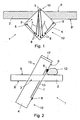
- a generally designated 1 chip arrangement has a substrate plate 2 with an opening 3, in which a carrier chip 4 is inserted.
- the substrate plate 2 may for example consist of glass or a semiconductor material.
- the carrier chip 4 has a plurality of electronic components 5 designed as sensors, which are integrated into the carrier chip 4 on a flat-side surface 6 of the carrier chip 4 using methods of semiconductor technology.
- the individual components 5 are connected in each case with a conductor track 7 running on the surface 6 of the carrier chip 4 or substantially parallel thereto to a connection contact 8 to which an evaluation and control device can be connected. As can be seen particularly clearly from FIG.
- the carrier chip 4 is inserted into the opening 3 of the substrate plate 2 in such a way that its ends project beyond the flat-side surfaces 9, 9 'of the substrate plate 2 facing away from one another, thereby forming projections 10, 10', which project on the flat-side surfaces 9, 9 'of the substrate plate 2.
- the components 5 are arranged on the one projection 10 and the respectively associated electrical connection contacts 8 on the other projection 10 '.
- terminal contacts 8 are good against a on the components 5 facing the front of the substrate plate 2 befindliches, with the sensors designed as components 5 to be examined medium, which may be, for example, a nutrient medium 11 with therein biological cells , shielded. Corrosion at the terminal contacts 8 by ingredients contained in the nutrient medium 11, such as salts or ions, is thereby reliably avoided.
- the chip assembly 1 is characterized simple and inexpensive to produce.
- the carrier chip 4 is formed as a rectangular plate, which is arranged with its chip plane and its transverse thereto extending narrow side surfaces each perpendicular to the flat side surfaces 9, 9 'of the substrate plate 2.
- the breakthrough 3 limiting surfaces of the substrate plate 2 are each perpendicular to their flat-side surfaces 9, 9 'are arranged.
- the carrier chip surface 6 having the component 5 and the terminal contact 8 is at a right angle to the flat side surfaces 9, 9 'of the substrate plate 2 extending plane obliquely to these surfaces 9, 9' and closes with this an acute angle ⁇ .
- the component 5 is arranged on the flat-side surface 6 of the carrier chip 4 at a distance from the edges of this surface 6.
- the access area to the component 5 is thus limited by the carrier chip 4 and the substrate plate 2, wherein the opening angle ⁇ of the access area is selected so that particles exceeding a predetermined size are kept away from the component 5.
- the component 5 may be, for example, a glucose sensor or lactate sensor.
- the device 5 may also be a Clark cell based oxygen sensor, a nitrogen sensor, an ion concentration sensor, or a thermocouple.
- a component 5 which emits an electric or electromagnetic field with which a cell located on the substrate plate 2 can be influenced or stimulated.
- the conductor tracks 7 are covered with an electrically insulating thin-film passivation layer 13, which may for example consist of silicon oxide. Through the passivation layer 13, the conductor tracks 7 are electrically well insulated against the nutrient medium 11. In addition, the passivation layer 13 prevents corrosion on the printed conductors 7 by salts or ions contained in the nutrient medium 11.
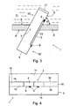
- the carrier chip 4 embodied as an approximately square plate has two electronic components 5 integrated in the carrier chip 4 at this corner region, which are connected by means of conductor tracks 7 to terminal contacts 8 which are connected to the latter Components 5 remote flat side surface 9 of the substrate plate 2 located supernatant 10 'of the carrier chip 4 are arranged.
- the formed as sensors 5 components projecting projection 10 of the carrier chip 4 can be inserted into a soft body to be examined, for example, a skin layer, the flat-side surface 9 of the substrate plate 2 serves as a stop surface for the body, which is the insertion depth of the pointed projection 10th limited in the body.
- the components 5 it is possible to position the components 5 in a defined manner in a defined depth determined by the protrusion dimension of the supernatant 10 in the body or medium to be examined in a simple manner.
- the carrier chip 4 is used in the mounting of the substrate plate 2 in three different rotational positions with respect to the surface normal to the carrier chip level in the approximately trapezoidal in cross-section opening 3 of the substrate plate 2, wherein in the individual rotational positions in each case with supernatants different components 5 are arranged in the position of use in the measurement object facing flat side surface 9 of the substrate plate 2 and these components 5 are each connected by means of the breakthrough 3-enforcing interconnects 7 with terminal contacts 8, facing away from the opposite to be examined to the test object flat side surface 9 'located supernatant 10' are arranged.
- the carrier chip 4 different chip assemblies 1 are produced.
- the carrier chip In the chip plane, the carrier chip with its the substrate plate 2 passing edges arranged obliquely to the flat-side surface planes 9, 9 'of the substrate plate 2. In Fig. 1 it can be clearly seen that these edges of the carrier chip 4 are each inclined at about an angle of 45 ° relative to the surface planes 9, 9 '.
- FIG. 5 shows a chip arrangement whose substrate plate 2 has openings 3 for two mutually associated carrier chips 4, one of the carrier chips 4 having as component 5 an optical transmitter and the other carrier chip 4 having an optical receiver. Between the optical transmitter and the receiver, a measuring path is formed.
- the chip arrangement can be used for example for transmitted light or scattered light measurement and / or as a light barrier.
- the substrate plate 2 has four plate parts arranged in a plane, namely two first plate parts 14 and two second plate parts 15.
- the first plate parts 14 each have a straight edge region 16, with which they are arranged parallel to one another and facing each other
- the second plate parts 15 are arranged side by side in the extension direction of the straight edge regions 16, spaced apart from each other by the aperture 3 between the first plate parts 14 and adhesively bonded to a straight edge region 16 of a first plate part 14 at their mutually parallel longitudinal edges.
- At least one of the second plate parts 15 is displaced in the plane of the plate parallel to the straight edge regions 16 of the first plate parts 14, to adapt the dimensions of the opening 3 to the respective position of the carrier chip 4.
- the end-side end region of the carrier chip 4 arranged transversely to the carrier chip extension plane is covered with an insulation layer 17 in the region of the projection 10 having the component 5.
Landscapes
- Engineering & Computer Science (AREA)
- Power Engineering (AREA)
- Physics & Mathematics (AREA)
- General Physics & Mathematics (AREA)
- Microelectronics & Electronic Packaging (AREA)
- Condensed Matter Physics & Semiconductors (AREA)
- Computer Hardware Design (AREA)
- Analytical Chemistry (AREA)
- Life Sciences & Earth Sciences (AREA)
- Chemical & Material Sciences (AREA)
- Health & Medical Sciences (AREA)
- Biochemistry (AREA)
- General Health & Medical Sciences (AREA)
- Immunology (AREA)
- Pathology (AREA)
- Measurement Of The Respiration, Hearing Ability, Form, And Blood Characteristics Of Living Organisms (AREA)
- Details Of Resistors (AREA)
- Structures For Mounting Electric Components On Printed Circuit Boards (AREA)
- Apparatus Associated With Microorganisms And Enzymes (AREA)
- Testing Of Individual Semiconductor Devices (AREA)
Claims (10)
- Agencement (1) de puce électronique qui présente une plaque de substrat (2) dans laquelle au moins une perforation (3) est ménagée et une puce de support (4) insérée ou destinée à être insérée dans la perforation (3), au moins une piste conductrice (7) qui relie au moins un composant électrique ou électronique (5) et en particulier un détecteur à au moins un contact (8) de raccordement électrique étant intégré à la surface de la puce de support, la puce de support (4) étant ou pouvant être insérée dans la perforation (3) de telle sorte que ses extrémités débordent au-dessus des surfaces planes (9, 9') non tournées l'une vers l'autre de la plaque de substrat (2) et forment ainsi des saillies (10, 10'), le composant étant disposé sur la saillie (10) qui déborde de la surface (9) et le contact de raccordement (8) étant disposé sur la saillie (10') qui déborde de l'autre surface (9'), la piste conductrice (7) reliant le composant (5) et le contact de raccordement (8) en traversant la perforation (3) de la plaque de substrat (2), un joint d'étanchéité étant prévu entre la plaque de substrat (2) et la puce de support (4), caractérisé en ce que partant de la surface (9) de la plaque de substrat (2), la section transversale de la saillie (10) qui présente le composant électrique ou électronique (5) se rétrécit en direction de l'emplacement le plus en débord de la saillie (10) de telle sorte que la saillie puisse être enfoncée dans un corps mou à étudier ou à traiter.
- Agencement (1) de puce électronique selon la revendication 1, caractérisé en ce que la puce de support (4) peut être reliée de manière libérable à la plaque de substrat (2).
- Agencement (1) de puce électronique selon la revendication 1 ou 2, caractérisé en ce qu'au moins dans la zone de la saillie (10) qui présente le composant électrique ou électronique (5), la ou les pistes conductrices (7) sont recouvertes d'une couche de passivation en film mince électriquement isolant.
- Agencement (1) de puce électronique selon l'une quelconque des revendications 1 à 3, caractérisé en ce que lors du montage de l'agencement (1) de puce électronique, la puce de support (4) peut être insérée en au moins deux positions différentes dans la perforation (3) ménagée dans la plaque de substrat (2), en ce que dans une de ces positions, au moins un composant électrique ou électronique (5) est disposé sur une saillie (10) de la puce de support (4) qui déborde de la surface plane de la plaque de substrat (9) et le ou les contacts de raccordement (8) associés à ce ou à ces composants (5) sont disposés sur la saillie (10') qui déborde de l'autre surface plane (9') de la plaque de substrat et en ce que, lorsque la puce de support (4) est dans l'autre position, le ou les composants (5) et le ou les contacts de raccordement (8) sont disposés respectivement sur la même saillie (10, 10') de la puce de support (4) qui déborde d'une surface plane de la plaque de substrat (9, 9').
- Agencement (1) de puce électronique selon l'une quelconque des revendications 1 à 4, caractérisé en ce que lors du montage de l'agencement (1) de puce électronique, la puce de support (4) peut être insérée en au moins deux positions différentes dans la perforation (3) de la plaque de substrat (2), en ce que la puce de support (4) présente au moins deux composants électriques ou électroniques (5) qui sont tous reliés au moyen d'au moins d'une piste conductrice (7) à au moins un contact d'un raccordement électrique (8) respectif associé, en ce que selon la position que l'on a sélectionnée pour la puce de support (4), chaque fois au moins un de ces composants (5) est disposé sur une saillie (10) de la puce de support (4) qui déborde d'une surface plane de la plaque de substrat (9) et en ce que le ou les contacts de raccordement (8) associés à ce ou ces composants (5) sont disposés sur la saillie (10') qui déborde de l'autre surface plane (9') de la plaque de substrat.
- Agencement (1) de puce électronique selon l'une quelconque des revendications 1 à 5, caractérisé en ce que sur la puce de support (4) repose un corps qui recouvre le composant électrique ou électronique (5), et en ce qu'au moins une zone adjacente au corps et qui déborde latéralement du plan de la surface du composant (5) et/ou une zone adjacente à la zone de la puce de support (4), au corps, et qui déborde latéralement de la partie de la surface recouvrant le composant (5) sont disposées comme écarteurs sur la puce de support (4), de manière à former un espace libre ou un interstice qui forme entre le composant (5) et le corps un accès au composant.
- Agencement (1) de puce électronique selon l'une quelconque des revendications 1 à 6, caractérisé en ce que dans la zone de l'espace de mesure ou d'action du composant électrique ou électronique (5), la plaque de substrat (2) présente au moins une saillie qui forme un filtre mécanique avec la saillie (10) qui présente le composant (5).
- Agencement (1) de puce électronique selon l'une quelconque des revendications 1 à 7, caractérisé en ce que la surface de la puce de support qui présente le composant électrique ou électronique (5) et la surface tournée vers celle-ci de la saillie disposée dans la zone de l'espace de mesure ou d'action du composant (5) s'étendent obliquement l'une par rapport à l'autre en forme d'entonnoir dans le plan de la surface de la plaque de substrat (2).
- Agencement (1) de puce électronique selon l'une quelconque des revendications 1 à 8, caractérisé en ce qu'au moins deux puces de support (4) sont insérées dans la plaque de substrat (2), en ce que l'une des puces de support (4) présente au moins un composant (5) configuré comme émetteur de rayonnement, en ce que l'autre puce de support (4) présente au moins un composant (5) configuré comme récepteur associé à l'émetteur de rayonnement et en ce qu'un parcours de mesure est disposé entre l'émetteur de rayonnement et le récepteur.
- Agencement (1) de puce électronique selon l'une quelconque des revendications 1 à 9, caractérisé en ce que le composant électrique ou électronique (5) est relié à une unité d'évaluation et/ou de commande intégrée dans la puce de support (4).
Applications Claiming Priority (3)
| Application Number | Priority Date | Filing Date | Title |
|---|---|---|---|
| DE19829121A DE19829121C2 (de) | 1998-06-30 | 1998-06-30 | Anordnung mit einer Substratplatte und einem Chip |
| DE19829121 | 1998-06-30 | ||
| EP99112071A EP0969510B1 (fr) | 1998-06-30 | 1999-06-23 | Agencement d'une puce électronique |
Related Parent Applications (1)
| Application Number | Title | Priority Date | Filing Date |
|---|---|---|---|
| EP99112071A Division EP0969510B1 (fr) | 1998-06-30 | 1999-06-23 | Agencement d'une puce électronique |
Publications (3)
| Publication Number | Publication Date |
|---|---|
| EP1189281A2 EP1189281A2 (fr) | 2002-03-20 |
| EP1189281A3 EP1189281A3 (fr) | 2005-12-07 |
| EP1189281B1 true EP1189281B1 (fr) | 2007-08-22 |
Family
ID=26047125
Family Applications (2)
| Application Number | Title | Priority Date | Filing Date |
|---|---|---|---|
| EP01126916A Expired - Lifetime EP1189281B1 (fr) | 1998-06-30 | 1999-06-23 | Agencement de puce électronique |
| EP01126917A Withdrawn EP1199751A3 (fr) | 1998-06-30 | 1999-06-23 | Agencement de puce électronique |
Family Applications After (1)
| Application Number | Title | Priority Date | Filing Date |
|---|---|---|---|
| EP01126917A Withdrawn EP1199751A3 (fr) | 1998-06-30 | 1999-06-23 | Agencement de puce électronique |
Country Status (1)
| Country | Link |
|---|---|
| EP (2) | EP1189281B1 (fr) |
Cited By (1)
| Publication number | Priority date | Publication date | Assignee | Title |
|---|---|---|---|---|
| DE102014108356A1 (de) | 2014-06-13 | 2015-12-17 | Innovative Sensor Technology Ist Ag | Planares Heizelement mit einer PTC-Widerstandsstruktur |
Families Citing this family (1)
| Publication number | Priority date | Publication date | Assignee | Title |
|---|---|---|---|---|
| US6228819B1 (en) | 1994-04-14 | 2001-05-08 | Rohm And Haas Company | Process for making a viscosity index improving copolymer |
Family Cites Families (10)
| Publication number | Priority date | Publication date | Assignee | Title |
|---|---|---|---|---|
| DE2736200A1 (de) * | 1977-08-11 | 1979-02-22 | Bbc Brown Boveri & Cie | Chemisch sensitiver feldeffekt- transistor und verfahren zur herstellung desselben |
| CA1250020A (fr) * | 1985-01-23 | 1989-02-14 | Imants R. Lauks | Detecteur de milieu |
| EP0261208A4 (fr) * | 1986-03-21 | 1988-10-27 | Integrated Ionics Inc | Dispositifs transducteurs captant des conditions ambiantes et pourvus d'une isolation. |
| DK409188D0 (da) * | 1988-07-21 | 1988-07-21 | Radiometer As | Fremgangsmaade til maaling af en karakteristik i et fluidum |
| US5046496A (en) * | 1989-04-26 | 1991-09-10 | Ppg Industries, Inc. | Sensor assembly for measuring analytes in fluids |
| DE4033741C2 (de) * | 1989-11-02 | 1994-03-31 | Falko Volkhardt E Dipl Tittel | Vorrichtung zum Nachweis von HIV-Antikörpern im Vollblut mit Anzeige des Ergebnisses |
| DE4013593A1 (de) * | 1990-04-27 | 1991-10-31 | Biotechnolog Forschung Gmbh | Verfahren und sensor fuer amperometrische messprinzipien mit dickschicht-biosensoren |
| SE511634C2 (sv) * | 1996-05-07 | 1999-11-01 | Samba Sensors Ab | Anordning för elektrooptisk mätning av tryck |
| DE19621227C2 (de) * | 1996-05-25 | 2003-02-20 | Micronas Gmbh | Sensorelement zum Nachweis von flüssigen, gasförmigen oder fluiden Substanzen |
| DE69722414T2 (de) * | 1996-07-03 | 2004-05-19 | Altea Therapeutics Corp. | Mehrfache mechanische mikroperforierung von haut oder schleimhäuten |
-
1999
- 1999-06-23 EP EP01126916A patent/EP1189281B1/fr not_active Expired - Lifetime
- 1999-06-23 EP EP01126917A patent/EP1199751A3/fr not_active Withdrawn
Non-Patent Citations (1)
| Title |
|---|
| None * |
Cited By (1)
| Publication number | Priority date | Publication date | Assignee | Title |
|---|---|---|---|---|
| DE102014108356A1 (de) | 2014-06-13 | 2015-12-17 | Innovative Sensor Technology Ist Ag | Planares Heizelement mit einer PTC-Widerstandsstruktur |
Also Published As
| Publication number | Publication date |
|---|---|
| EP1199751A2 (fr) | 2002-04-24 |
| EP1189281A2 (fr) | 2002-03-20 |
| EP1189281A3 (fr) | 2005-12-07 |
| EP1199751A3 (fr) | 2005-12-07 |
Similar Documents
| Publication | Publication Date | Title |
|---|---|---|
| DE60114159T2 (de) | Messung von stoffen in flüssigkeiten | |
| EP1035918B1 (fr) | Dispositif de mesure de parametres physiologiques | |
| DE69208948T2 (de) | Ph-elektrode | |
| DE19907164C2 (de) | Meßeinrichtung sowie Verfahren zu deren Herstellung | |
| DE102006055797B4 (de) | Sensorelement für einen Gasssensor zur Bestimmung einer physikalischen Eigenschaft eines Messgases | |
| WO2004017829A2 (fr) | Système d'électrode de mesure | |
| EP1003035A2 (fr) | Dispositif de mesure | |
| EP2445391B1 (fr) | Capteur pour mesures in-vivo | |
| EP0382831B1 (fr) | Transducteur chimiquement sensible | |
| EP1236037B1 (fr) | Capteur place dans un boitier | |
| EP1189281B1 (fr) | Agencement de puce électronique | |
| DE2736200A1 (de) | Chemisch sensitiver feldeffekt- transistor und verfahren zur herstellung desselben | |
| EP1695067B1 (fr) | Détecteur de turbidité | |
| DE19861113C2 (de) | Anordnung mit einer Substratplatte und einem Chip | |
| DE19829121C2 (de) | Anordnung mit einer Substratplatte und einem Chip | |
| DE102004010635A1 (de) | Vorrichtung zur Durchführung von Messungen an Biokomponenten | |
| DE69002327T2 (de) | Leitfähigkeits- oder kapazitätszelle und ein verfahren zu deren herstellung und eine sonde mit so einer zelle und ein verfahren zur messung der relativen feuchtigkeit mit so einer sonde. | |
| DE3728848C2 (de) | Elektrochemischer gassensor | |
| EP1055122B1 (fr) | Composant pour mesurer la concentration de gaz | |
| EP0538432B1 (fr) | Dispositif pour la realisation d'un circuit electrique, en particulier pour une sonde de mesure, et sonde de mesure | |
| DE3115961C2 (de) | Hygrometer | |
| DE102023104705A1 (de) | Plasma-Behandlungsanordnung | |
| DE3440180C2 (fr) | ||
| DE29780368U1 (de) | Probenehmer für Flüssigkeiten | |
| DE102019220431A1 (de) | Vorrichtung zur Messung der hygrometrischen Feuchtigkeit in Baustoffen |
Legal Events
| Date | Code | Title | Description |
|---|---|---|---|
| PUAI | Public reference made under article 153(3) epc to a published international application that has entered the european phase |
Free format text: ORIGINAL CODE: 0009012 |
|
| AC | Divisional application: reference to earlier application |
Ref document number: 969510 Country of ref document: EP |
|
| AK | Designated contracting states |
Kind code of ref document: A2 Designated state(s): AT BE CH CY DE DK ES FI FR GB GR IE IT LI LU MC NL PT SE |
|
| RIN1 | Information on inventor provided before grant (corrected) |
Inventor name: SIEBEN, ULRICH DR. Inventor name: LEHMANN, MIRKO DIPL.-PHYS. Inventor name: GAHLE, HANS-JUERGEN DR. Inventor name: EHRET, RALF DR. Inventor name: BAUMANN, WERNER DR. Inventor name: IGEL, GUENTER DIPL.-ING. |
|
| PUAL | Search report despatched |
Free format text: ORIGINAL CODE: 0009013 |
|
| RIC1 | Information provided on ipc code assigned before grant |
Ipc: 7G 01N 33/487 B Ipc: 7H 01L 25/065 A Ipc: 7H 01L 25/07 B Ipc: 7A 61B 5/00 B Ipc: 7G 01N 27/414 B Ipc: 7G 01N 27/403 B Ipc: 7A 61M 37/00 B Ipc: 7G 01N 27/28 B |
|
| AK | Designated contracting states |
Kind code of ref document: A3 Designated state(s): AT BE CH CY DE DK ES FI FR GB GR IE IT LI LU MC NL PT SE |
|
| 17P | Request for examination filed |
Effective date: 20060117 |
|
| AKX | Designation fees paid |
Designated state(s): CH DE FR GB IT LI NL |
|
| GRAP | Despatch of communication of intention to grant a patent |
Free format text: ORIGINAL CODE: EPIDOSNIGR1 |
|
| GRAS | Grant fee paid |
Free format text: ORIGINAL CODE: EPIDOSNIGR3 |
|
| GRAA | (expected) grant |
Free format text: ORIGINAL CODE: 0009210 |
|
| AC | Divisional application: reference to earlier application |
Ref document number: 0969510 Country of ref document: EP Kind code of ref document: P |
|
| AK | Designated contracting states |
Kind code of ref document: B1 Designated state(s): CH DE FR GB IT LI NL |
|
| REG | Reference to a national code |
Ref country code: GB Ref legal event code: FG4D Free format text: NOT ENGLISH |
|
| REG | Reference to a national code |
Ref country code: CH Ref legal event code: EP |
|
| REG | Reference to a national code |
Ref country code: CH Ref legal event code: NV Representative=s name: PATENTANWALT DIPL. ING. WOLFGANG HEISEL |
|
| REF | Corresponds to: |
Ref document number: 59914473 Country of ref document: DE Date of ref document: 20071004 Kind code of ref document: P |
|
| GBT | Gb: translation of ep patent filed (gb section 77(6)(a)/1977) |
Effective date: 20071001 |
|
| ET | Fr: translation filed | ||
| PLBE | No opposition filed within time limit |
Free format text: ORIGINAL CODE: 0009261 |
|
| STAA | Information on the status of an ep patent application or granted ep patent |
Free format text: STATUS: NO OPPOSITION FILED WITHIN TIME LIMIT |
|
| 26N | No opposition filed |
Effective date: 20080526 |
|
| REG | Reference to a national code |
Ref country code: CH Ref legal event code: PCAR Free format text: PATENTANWALT DIPL.-ING. (UNI.) WOLFGANG HEISEL;HAUPTSTRASSE 14;8280 KREUZLINGEN (CH) |
|
| PGFP | Annual fee paid to national office [announced via postgrant information from national office to epo] |
Ref country code: FR Payment date: 20100706 Year of fee payment: 12 |
|
| PGFP | Annual fee paid to national office [announced via postgrant information from national office to epo] |
Ref country code: IT Payment date: 20100625 Year of fee payment: 12 |
|
| PGFP | Annual fee paid to national office [announced via postgrant information from national office to epo] |
Ref country code: NL Payment date: 20100614 Year of fee payment: 12 |
|
| PGFP | Annual fee paid to national office [announced via postgrant information from national office to epo] |
Ref country code: GB Payment date: 20100618 Year of fee payment: 12 Ref country code: DE Payment date: 20100625 Year of fee payment: 12 |
|
| REG | Reference to a national code |
Ref country code: DE Ref legal event code: R082 Ref document number: 59914473 Country of ref document: DE |
|
| REG | Reference to a national code |
Ref country code: NL Ref legal event code: V1 Effective date: 20120101 |
|
| GBPC | Gb: european patent ceased through non-payment of renewal fee |
Effective date: 20110623 |
|
| PG25 | Lapsed in a contracting state [announced via postgrant information from national office to epo] |
Ref country code: IT Free format text: LAPSE BECAUSE OF NON-PAYMENT OF DUE FEES Effective date: 20110623 |
|
| REG | Reference to a national code |
Ref country code: FR Ref legal event code: ST Effective date: 20120229 |
|
| REG | Reference to a national code |
Ref country code: DE Ref legal event code: R119 Ref document number: 59914473 Country of ref document: DE Effective date: 20120103 |
|
| PG25 | Lapsed in a contracting state [announced via postgrant information from national office to epo] |
Ref country code: DE Free format text: LAPSE BECAUSE OF NON-PAYMENT OF DUE FEES Effective date: 20120103 Ref country code: FR Free format text: LAPSE BECAUSE OF NON-PAYMENT OF DUE FEES Effective date: 20110630 |
|
| PG25 | Lapsed in a contracting state [announced via postgrant information from national office to epo] |
Ref country code: NL Free format text: LAPSE BECAUSE OF NON-PAYMENT OF DUE FEES Effective date: 20120101 |
|
| REG | Reference to a national code |
Ref country code: CH Ref legal event code: PUE Owner name: ENDRESS+HAUSER GESELLSCHAFT FUER MESS- UND REGELT Free format text: MICRONAS GMBH#HANS-BUNTE-STRASSE 19#79008 FREIBURG (DE) -TRANSFER TO- ENDRESS+HAUSER GESELLSCHAFT FUER MESS- UND REGELTECHNIK MBH+CO.KG#DIESELSTRASSE 24#70839 GERLINGEN (DE) |
|
| PG25 | Lapsed in a contracting state [announced via postgrant information from national office to epo] |
Ref country code: GB Free format text: LAPSE BECAUSE OF NON-PAYMENT OF DUE FEES Effective date: 20110623 |
|
| REG | Reference to a national code |
Ref country code: CH Ref legal event code: PUE Owner name: INNOVATIVE SENSOR TECHNOLOGY IST AG Free format text: ENDRESS+HAUSER GESELLSCHAFT FUER MESS- UND REGELTECHNIK MBH+CO.KG#DIESELSTRASSE 24#70839 GERLINGEN (DE) -TRANSFER TO- INNOVATIVE SENSOR TECHNOLOGY IST AG#INDUSTRIESTRASSE 2#9630 WATTWIL (CH) |
|
| REG | Reference to a national code |
Ref country code: CH Ref legal event code: PCOW Free format text: NEW ADDRESS: STEGRUETISTRASSE 14, 9642 EBNAT-KAPPEL (CH) |
|
| PGFP | Annual fee paid to national office [announced via postgrant information from national office to epo] |
Ref country code: CH Payment date: 20180621 Year of fee payment: 20 |
|
| REG | Reference to a national code |
Ref country code: CH Ref legal event code: PL |