EP1189281B1 - Chip-arrangement - Google Patents
Chip-arrangement Download PDFInfo
- Publication number
- EP1189281B1 EP1189281B1 EP01126916A EP01126916A EP1189281B1 EP 1189281 B1 EP1189281 B1 EP 1189281B1 EP 01126916 A EP01126916 A EP 01126916A EP 01126916 A EP01126916 A EP 01126916A EP 1189281 B1 EP1189281 B1 EP 1189281B1
- Authority
- EP
- European Patent Office
- Prior art keywords
- substrate plate
- chip
- component
- projection
- support chip
- Prior art date
- Legal status (The legal status is an assumption and is not a legal conclusion. Google has not performed a legal analysis and makes no representation as to the accuracy of the status listed.)
- Expired - Lifetime
Links
Images

Classifications
-
- H—ELECTRICITY
- H01—ELECTRIC ELEMENTS
- H01L—SEMICONDUCTOR DEVICES NOT COVERED BY CLASS H10
- H01L23/00—Details of semiconductor or other solid state devices
- H01L23/52—Arrangements for conducting electric current within the device in operation from one component to another, i.e. interconnections, e.g. wires, lead frames
- H01L23/538—Arrangements for conducting electric current within the device in operation from one component to another, i.e. interconnections, e.g. wires, lead frames the interconnection structure between a plurality of semiconductor chips being formed on, or in, insulating substrates
- H01L23/5385—Assembly of a plurality of insulating substrates
-
- G—PHYSICS
- G01—MEASURING; TESTING
- G01N—INVESTIGATING OR ANALYSING MATERIALS BY DETERMINING THEIR CHEMICAL OR PHYSICAL PROPERTIES
- G01N21/00—Investigating or analysing materials by the use of optical means, i.e. using sub-millimetre waves, infrared, visible or ultraviolet light
- G01N21/01—Arrangements or apparatus for facilitating the optical investigation
-
- H—ELECTRICITY
- H01—ELECTRIC ELEMENTS
- H01L—SEMICONDUCTOR DEVICES NOT COVERED BY CLASS H10
- H01L25/00—Assemblies consisting of a plurality of individual semiconductor or other solid state devices ; Multistep manufacturing processes thereof
- H01L25/03—Assemblies consisting of a plurality of individual semiconductor or other solid state devices ; Multistep manufacturing processes thereof all the devices being of a type provided for in the same subgroup of groups H01L27/00 - H01L33/00, or in a single subclass of H10K, H10N, e.g. assemblies of rectifier diodes
- H01L25/04—Assemblies consisting of a plurality of individual semiconductor or other solid state devices ; Multistep manufacturing processes thereof all the devices being of a type provided for in the same subgroup of groups H01L27/00 - H01L33/00, or in a single subclass of H10K, H10N, e.g. assemblies of rectifier diodes the devices not having separate containers
- H01L25/07—Assemblies consisting of a plurality of individual semiconductor or other solid state devices ; Multistep manufacturing processes thereof all the devices being of a type provided for in the same subgroup of groups H01L27/00 - H01L33/00, or in a single subclass of H10K, H10N, e.g. assemblies of rectifier diodes the devices not having separate containers the devices being of a type provided for in group H01L29/00
-
- A—HUMAN NECESSITIES
- A61—MEDICAL OR VETERINARY SCIENCE; HYGIENE
- A61B—DIAGNOSIS; SURGERY; IDENTIFICATION
- A61B5/00—Measuring for diagnostic purposes; Identification of persons
- A61B5/145—Measuring characteristics of blood in vivo, e.g. gas concentration, pH value; Measuring characteristics of body fluids or tissues, e.g. interstitial fluid, cerebral tissue
- A61B5/14532—Measuring characteristics of blood in vivo, e.g. gas concentration, pH value; Measuring characteristics of body fluids or tissues, e.g. interstitial fluid, cerebral tissue for measuring glucose, e.g. by tissue impedance measurement
-
- A—HUMAN NECESSITIES
- A61—MEDICAL OR VETERINARY SCIENCE; HYGIENE
- A61B—DIAGNOSIS; SURGERY; IDENTIFICATION
- A61B5/00—Measuring for diagnostic purposes; Identification of persons
- A61B5/145—Measuring characteristics of blood in vivo, e.g. gas concentration, pH value; Measuring characteristics of body fluids or tissues, e.g. interstitial fluid, cerebral tissue
- A61B5/1468—Measuring characteristics of blood in vivo, e.g. gas concentration, pH value; Measuring characteristics of body fluids or tissues, e.g. interstitial fluid, cerebral tissue using chemical or electrochemical methods, e.g. by polarographic means
- A61B5/1473—Measuring characteristics of blood in vivo, e.g. gas concentration, pH value; Measuring characteristics of body fluids or tissues, e.g. interstitial fluid, cerebral tissue using chemical or electrochemical methods, e.g. by polarographic means invasive, e.g. introduced into the body by a catheter
-
- A—HUMAN NECESSITIES
- A61—MEDICAL OR VETERINARY SCIENCE; HYGIENE
- A61B—DIAGNOSIS; SURGERY; IDENTIFICATION
- A61B5/00—Measuring for diagnostic purposes; Identification of persons
- A61B5/44—Detecting, measuring or recording for evaluating the integumentary system, e.g. skin, hair or nails
- A61B5/441—Skin evaluation, e.g. for skin disorder diagnosis
-
- G—PHYSICS
- G01—MEASURING; TESTING
- G01N—INVESTIGATING OR ANALYSING MATERIALS BY DETERMINING THEIR CHEMICAL OR PHYSICAL PROPERTIES
- G01N33/00—Investigating or analysing materials by specific methods not covered by groups G01N1/00 - G01N31/00
- G01N33/48—Biological material, e.g. blood, urine; Haemocytometers
- G01N33/483—Physical analysis of biological material
- G01N33/487—Physical analysis of biological material of liquid biological material
- G01N33/48707—Physical analysis of biological material of liquid biological material by electrical means
-
- H—ELECTRICITY
- H01—ELECTRIC ELEMENTS
- H01L—SEMICONDUCTOR DEVICES NOT COVERED BY CLASS H10
- H01L2924/00—Indexing scheme for arrangements or methods for connecting or disconnecting semiconductor or solid-state bodies as covered by H01L24/00
- H01L2924/0001—Technical content checked by a classifier
- H01L2924/0002—Not covered by any one of groups H01L24/00, H01L24/00 and H01L2224/00
Definitions
- the invention relates to a chip arrangement with a substrate plate which has at least one opening into which a carrier chip is inserted or used, which has at least one integrated conductor track on a carrier chip surface, which has at least one electrical or electronic component, in particular a sensor. connects with at least one electrical connection contact, wherein the carrier chip is inserted or insertable in the breakthrough that it projects beyond the opposite flat side surfaces of the substrate plate with its ends and thereby forms supernatants, wherein on the one surface protruding supernatant the device and on the the other surface protruding supernatant of the terminal contact is arranged, wherein the component and the terminal contact interconnecting interconnect passes through the breakthrough of the substrate plate, and wherein between the substrate plate and the carrier chip before a seal is seen.
- the arrangement has a housing which delimits a measuring chamber, which is flowed through by the liquid to be examined.
- the housing In a housing wall, the housing has an opening into which a carrier chip is inserted, which has three components designed as microsensors, which are connected via conductor tracks with terminal contacts of the carrier chip.
- the carrier chip is inserted into the opening in such a way that with its ends it projects beyond the opposite sides of the housing wall and thereby forms projections.
- the terminal contacts are arranged at the end lying in the measuring chamber.
- the interconnect the components with the terminal interconnects interconnects enforce the breakthrough of the housing wall.
- the solution to this problem consists in an arrangement of the type mentioned above in that the cross section of the electrical or electronic component having supernatant tapering, starting from the surface of the substrate plate to the most prominent point of the supernatant.
- the supernatant having the component thus has a tip and can thereby be inserted into a soft body to be examined or treated
- the flat-sided surface of the substrate plate acting as a stop surface for the Body serves, which limits the insertion depth of the pointed protrusion in the body. This makes it possible to easily position the components in a defined, predetermined by the Sprintstands the supernatant depth in the body or medium to be examined.
- the substrate plate can be placed with its flat side, for example, on a skin layer to be examined, wherein the sensor having tip projection penetrates the depth corresponding to the height of the supernatant defined depth in the skin layer , so that there measurements can be taken.
- the glucose concentration, the moisture of the skin, an ion concentration, a gas content or the like physiological parameters can be measured, which make statements about the vitality of the skin and / or the underlying tissue area. It is even possible that the voltage applied to the skin layer substrate plate is moved parallel to the surface of the skin layer, so that the sensor having the supernatant is pulled parallel to the surface of the skin layer therethrough. As a result, a measuring profile can be created in a simple manner along a line running parallel to the surface of the skin layer.
- the electrical or electronic component is arranged on the supernatant located on one substrate plate surface and the terminal contact connected therewith via the conductor track integrated in the carrier chip, on the supernatant located on the other substrate plate surface.
- the terminal contact is thus located on the back of the substrate plate facing away from the electrical or electronic component, so that the interconnect areas located in the region of the component having the supernatant can be completely covered with a passivation layer.
- a passivation layer For example, in thin-film technology, it can be manufactured with high accuracy and moisture resistance, so that corrosion on the printed circuit integrated circuit trace is largely avoided by the medium to be examined or treated with the electrical or electronic component.
- the seal arranged between the carrier chip and the substrate plate prevents the medium located on the front side of the substrate plate from reaching the terminal contact arranged on the rear side of the substrate plate.
- the breakthrough arranged in the substrate plate can be introduced into the substrate plate, for example by means of ultrasonic drilling.
- the chip arrangement is thus easy and inexpensive to produce. Since a plastic material for pouring bond pads can be omitted, the chip arrangement also has particularly compact dimensions.
- the carrier chip is detachably connectable to the substrate plate. If necessary, the carrier chip can be easily replaced if the component has reached its intended service life or if it should fail due to contact with a chemically aggressive medium to be examined or treated.
- the carrier chip is adhesively bonded to a wall region of the substrate plate which delimits the aperture.
- the adhesive arranged between the carrier chip and the substrate plate then serves, on the one hand, to fix the carrier chip to the substrate plate and, on the other hand, also seals the breakthrough of the substrate plate against the carrier chip, so that one on the front side of the substrate plate in the region of the electrical or electronic component befindliches medium not to the terminal contact having the back Substrate plate can get.
- the adhesive also compensates for tolerances in the dimensions of the carrier chip and / or the wall opening in the substrate plate into which the carrier chip is inserted. The chip arrangement is thereby even easier and cheaper to produce.
- the carrier chip is arranged with its plane of extension perpendicular to a flat-side surface of the substrate plate.
- the breakthrough limiting side surfaces of the substrate plate can then be arranged at right angles to the flat-sided surface, which facilitates the introduction of the breakthrough in the substrate plate.
- a particularly advantageous embodiment of the invention provides that the carrier chip surface having the electrical or electronic component is arranged obliquely to the flat side surface of the substrate plate and preferably encloses with this an acute angle.
- the electrical or electronic component is then arranged in a corner region delimited by the carrier chip and the substrate plate, so that only particles which do not exceed a size predetermined by the dimensions of the corner region can come into contact with the electrical or electronic component. This results in a simply constructed mechanical filter that prevents the penetration of larger particles to the device.
- An advantageous embodiment of the invention provides that the carrier chip is used in the assembly of the chip assembly in at least two different layers in the opening of the substrate plate, that in one of these layers at least one electrical or electronic component on a flat side surface of the substrate plate towering Got over the support chip and the (this) component (s) associated (n) terminal contact (s) is arranged on the projecting the other flat-side surface of the substrate plate supernatant, and in that in the other position of the carrier chip, the (the) component (s) e) and the (the) terminal contact (s) are arranged on the same, a flat-side surface of the substrate plate superior projection of the carrier chip.
- the carrier chip in the assembly of the chip assembly in at least two different layers in the breakthrough of the substrate plate is used, that the carrier chip has at least two electrical or electronic components, each by means of at least one conductor track At least one of these components, depending on the selected position of the carrier chip, respectively, is connected to a projection of the carrier chip projecting beyond a flat-sided surface of the substrate plate and the component (s) assigned to this (this) component (s) ( n) terminal on which the other flat-side surface of the substrate plate superior projection is arranged.
- the carrier chip depending on the selected position of the carrier chip another component or even several others Components arranged on the in use position the object to be examined or treated object supernatant of the carrier chip.
- the service life of the chip arrangement is correspondingly extended, since a component which has become unusable, for example, through prolonged contact with a chemically aggressive medium, can be easily replaced by a corresponding, functional function by correspondingly converting the carrier chip Component can be replaced.
- the carrier chip can also have different components from each other. This results in a kit for creating a chip arrangement, with which, depending on the selected position of the carrier chip in the breakthrough of the substrate plate different chip arrangements can be made.
- the electrical or electronic components can be distributed, for example, distributed on the circumference of the carrier chip in the flat-side surface, wherein the carrier chip can be used in different rotational positions with respect to the normal to this surface in the substrate plate.
- other components or sensors are then respectively arranged on the front side of the substrate plate, while the connection contacts associated therewith are in each case located on the rear side of the substrate plate.
- an ion-permeable membrane is arranged on the electrical or electronic component.
- ions can reach the component or the sensor, while other substances are kept away from the sensor by the membrane.
- the membrane is permeable only for certain ions, so that their concentration can be selectively measured in a medium to be examined.
- the membrane is after inserting the carrier chip in the substrate plate to the electrical or electronic component applied.
- the membrane material is first dissolved in a volatile liquid, for example in alcohol or acetone.
- the chip arrangement is aligned so that the device having surface of the carrier chip obliquely to the horizontal, in particular runs vertically.
- a small amount of liquid containing the membrane material is applied to the adjacent edge of the carrier chip extending transversely to the component having surface of the carrier chip, such that a part of this liquid by gravity from the front edge surface of the carrier chip on the on the transversely arranged surface of the carrier chip located electrical or electronic component flows, so that forms a thin liquid layer on this. After the evaporation of this liquid layer then remains on the electrical or electronic component, a membrane layer having a uniform thickness on the device.
- the substrate plate in the region of the measuring or active space of the electrical or electronic component at least one projection which forms a mechanical filter together with the component having the supernatant.
- an effective space in the case of a component emitting an electromagnetic radiation is understood as the space into which the component emits the radiation. Accordingly, in a device that emanates an electric and / or magnetic field, the space in which this field is effective is understood.
- the mechanical filter thus has a protrusion cooperating with the projection having the component, wherein a free space is arranged between the component and the projection, which forms the access to the component.
- the projection may also be a step or step located on the substrate plate.
- the projection of the mechanical filter is formed by the projection of a plate inserted into an opening of the substrate plate.
- the projection can then be mounted in the same manner on the substrate plate in the manufacture of the chip arrangement as the projection of the carrier chip having the electrical or electronic component.
- the chip arrangement is thereby even easier to produce.
- the projection of the mechanical filter may also be formed by the projection of a further carrier chip.
- a body bears against the carrier chip and covers the electrical or electronic component such that at least one laterally over the surface plane as a spacer on the carrier chip of the component projecting on the body and / or on the body is arranged laterally over the component covering the surface region protruding, abutting on the carrier chip area, such that between the component and the body, the access to the device forming free space or gap is arranged.
- the body during assembly of the chip assembly is easier and can be positioned with greater accuracy on the carrier chip.
- the region protruding from the component can be produced by known methods of semiconductor technology, for example in mask technology be made with great dimensional accuracy, which in particular allows the realization of small gaps or clearances between the device and the body with tight tolerances.
- the body which bears against the projecting carrier chip region may have a substantially planar surface region, which faces the component and is arranged parallel to its surface plane and preferably bears against the projecting carrier chip region.
- the body can be a second carrier chip which rests flat against the projecting region of the first carrier chip.
- the preparation of the relative to the device projecting carrier chip area can be done for example in such a way that in the surface of the carrier chip a recess is etched, in which the device is arranged or that at certain points of the surface of the carrier chip at least one layer is vapor-deposited or applied ,
- the carrier chip surface having the electrical or electronic component and the surface of the projection arranged in the region of the measuring or effective space of the component extend in a funnel shape at an angle to one another in the surface plane of the substrate plate. This results in a funnel-shaped channel which forms a flow direction-dependent filter for a medium located on the substrate plate.
- the distance between the electrical or electronic component and the (the) measuring or Wirkraums arranged projection (projections) is adapted to the diameter of a biological cell and preferably greater than 4 microns and less than 55 microns. This allows a cell between the electrical or electronic component having supernatant and the projection attach directly to the device, while particles whose dimensions are greater than the cell diameter are kept away from the device.
- the carrier chips are inserted into the substrate plate, if one of the carrier chips has at least one component designed as a radiation emitter and the other carrier chip has at least one component designed as a receiver assigned to the radiation emitter and if between the radiation emitter and the receiver is arranged a measuring path.
- a scattered light or transmitted light measurement can be performed.
- the two carrier chips may at the same time also form a mechanical filter, so that only particles up to a certain size predetermined by the spacing of the carrier chips can reach the measuring path.
- the substrate plate consists of an elastic material.
- the substrate plate can then be acted upon in the extension direction with a tensile or compressive force in order to change the distance between the supernatant of the carrier chip having the electrical or electronic component and a projection of the substrate plate forming this with a mechanical filter.
- the filter characteristic of the mechanical filter can be easily adapted to the size of the particles to be examined or treated.
- the substrate plate may also be formed as a bendable film. The chip arrangement is then even easier to handle.
- the chip arrangement can be produced even more cost-effectively if the substrate plate has at least four arranged in one plane Plate parts, when adjacent plate members are preferably connected to each other at their mutually facing edge regions, preferably by an adhesive bond, and when the breakthrough is formed by a free space located between the plate parts.
- expensive drilling of the aperture for example by means of ultrasound or a laser beam, can be dispensed with.
- a burr as it may occur, for example, when laser drilling, can be avoided.
- the individual plate parts preferably each have straight edges and can be cut, for example, by cutting or sawing.
- first plate parts each have at least one straight edge region, with which they are arranged parallel to one another and facing each other, and if at least two second plate parts are arranged spaced apart from each other by the aperture between the first plate parts in the extension direction of the straight edge regions. which are each connected at their mutually parallel edges with the straight edge regions of the first plate parts in particular by gluing.
- the abutting first and second plate parts can then be moved against each other before attaching the gluing in the direction of their straight edge regions, whereby the length of the located in the substrate plate breakthrough can be easily changed and adapted to the dimensions of the carrier chip to be inserted therein.
- the end-side end region of the carrier chip arranged transversely to the carrier chip extension plane is covered with an insulation layer at least in the region of the projection having the component.
- a circuit board may be arranged, which has connected to the terminal contacts or connectable connection points. This results in a particularly compact design.
- the printed circuit board may have, for example, an evaluation device and / or a control device and / or a power supply for the chip arrangement. This is protected at the back of the substrate plate from contact with a medium to be examined.
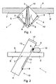
- a generally designated 1 chip arrangement has a substrate plate 2 with an opening 3, in which a carrier chip 4 is inserted.
- the substrate plate 2 may for example consist of glass or a semiconductor material.
- the carrier chip 4 has a plurality of electronic components 5 designed as sensors, which are integrated into the carrier chip 4 on a flat-side surface 6 of the carrier chip 4 using methods of semiconductor technology.
- the individual components 5 are connected in each case with a conductor track 7 running on the surface 6 of the carrier chip 4 or substantially parallel thereto to a connection contact 8 to which an evaluation and control device can be connected. As can be seen particularly clearly from FIG.
- the carrier chip 4 is inserted into the opening 3 of the substrate plate 2 in such a way that its ends project beyond the flat-side surfaces 9, 9 'of the substrate plate 2 facing away from one another, thereby forming projections 10, 10', which project on the flat-side surfaces 9, 9 'of the substrate plate 2.
- the components 5 are arranged on the one projection 10 and the respectively associated electrical connection contacts 8 on the other projection 10 '.
- terminal contacts 8 are good against a on the components 5 facing the front of the substrate plate 2 befindliches, with the sensors designed as components 5 to be examined medium, which may be, for example, a nutrient medium 11 with therein biological cells , shielded. Corrosion at the terminal contacts 8 by ingredients contained in the nutrient medium 11, such as salts or ions, is thereby reliably avoided.
- the chip assembly 1 is characterized simple and inexpensive to produce.
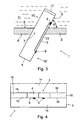
- the carrier chip 4 is formed as a rectangular plate, which is arranged with its chip plane and its transverse thereto extending narrow side surfaces each perpendicular to the flat side surfaces 9, 9 'of the substrate plate 2.
- the breakthrough 3 limiting surfaces of the substrate plate 2 are each perpendicular to their flat-side surfaces 9, 9 'are arranged.
- the carrier chip surface 6 having the component 5 and the terminal contact 8 is at a right angle to the flat side surfaces 9, 9 'of the substrate plate 2 extending plane obliquely to these surfaces 9, 9' and closes with this an acute angle ⁇ .
- the component 5 is arranged on the flat-side surface 6 of the carrier chip 4 at a distance from the edges of this surface 6.
- the access area to the component 5 is thus limited by the carrier chip 4 and the substrate plate 2, wherein the opening angle ⁇ of the access area is selected so that particles exceeding a predetermined size are kept away from the component 5.
- the component 5 may be, for example, a glucose sensor or lactate sensor.
- the device 5 may also be a Clark cell based oxygen sensor, a nitrogen sensor, an ion concentration sensor, or a thermocouple.
- a component 5 which emits an electric or electromagnetic field with which a cell located on the substrate plate 2 can be influenced or stimulated.
- the conductor tracks 7 are covered with an electrically insulating thin-film passivation layer 13, which may for example consist of silicon oxide. Through the passivation layer 13, the conductor tracks 7 are electrically well insulated against the nutrient medium 11. In addition, the passivation layer 13 prevents corrosion on the printed conductors 7 by salts or ions contained in the nutrient medium 11.
- the carrier chip 4 embodied as an approximately square plate has two electronic components 5 integrated in the carrier chip 4 at this corner region, which are connected by means of conductor tracks 7 to terminal contacts 8 which are connected to the latter Components 5 remote flat side surface 9 of the substrate plate 2 located supernatant 10 'of the carrier chip 4 are arranged.
- the formed as sensors 5 components projecting projection 10 of the carrier chip 4 can be inserted into a soft body to be examined, for example, a skin layer, the flat-side surface 9 of the substrate plate 2 serves as a stop surface for the body, which is the insertion depth of the pointed projection 10th limited in the body.
- the components 5 it is possible to position the components 5 in a defined manner in a defined depth determined by the protrusion dimension of the supernatant 10 in the body or medium to be examined in a simple manner.
- the carrier chip 4 is used in the mounting of the substrate plate 2 in three different rotational positions with respect to the surface normal to the carrier chip level in the approximately trapezoidal in cross-section opening 3 of the substrate plate 2, wherein in the individual rotational positions in each case with supernatants different components 5 are arranged in the position of use in the measurement object facing flat side surface 9 of the substrate plate 2 and these components 5 are each connected by means of the breakthrough 3-enforcing interconnects 7 with terminal contacts 8, facing away from the opposite to be examined to the test object flat side surface 9 'located supernatant 10' are arranged.
- the carrier chip 4 different chip assemblies 1 are produced.
- the carrier chip In the chip plane, the carrier chip with its the substrate plate 2 passing edges arranged obliquely to the flat-side surface planes 9, 9 'of the substrate plate 2. In Fig. 1 it can be clearly seen that these edges of the carrier chip 4 are each inclined at about an angle of 45 ° relative to the surface planes 9, 9 '.
- FIG. 5 shows a chip arrangement whose substrate plate 2 has openings 3 for two mutually associated carrier chips 4, one of the carrier chips 4 having as component 5 an optical transmitter and the other carrier chip 4 having an optical receiver. Between the optical transmitter and the receiver, a measuring path is formed.
- the chip arrangement can be used for example for transmitted light or scattered light measurement and / or as a light barrier.
- the substrate plate 2 has four plate parts arranged in a plane, namely two first plate parts 14 and two second plate parts 15.
- the first plate parts 14 each have a straight edge region 16, with which they are arranged parallel to one another and facing each other
- the second plate parts 15 are arranged side by side in the extension direction of the straight edge regions 16, spaced apart from each other by the aperture 3 between the first plate parts 14 and adhesively bonded to a straight edge region 16 of a first plate part 14 at their mutually parallel longitudinal edges.
- At least one of the second plate parts 15 is displaced in the plane of the plate parallel to the straight edge regions 16 of the first plate parts 14, to adapt the dimensions of the opening 3 to the respective position of the carrier chip 4.
- the end-side end region of the carrier chip 4 arranged transversely to the carrier chip extension plane is covered with an insulation layer 17 in the region of the projection 10 having the component 5.
Description
Die Erfindung betrifft eine Chip-Anordnung mit einer Substratplatte, die wenigstens einen Durchbruch aufweist, in den ein Trägerchip eingesetzt oder einsetzbar ist, der an einer Trägerchip-Oberfläche wenigstens eine integrierte Leiterbahn aufweist, die wenigstens ein elektrisches oder elektronisches Bauelement, insbesondere einen Sensor, mit zumindest einem elektrischen Anschlußkontakt verbindet, wobei der Trägerchip derart in den Durchbruch eingesetzt oder einsetzbar ist, daß er mit seinen Enden die einander abgewandten flachseitigen Oberflächen der Substratplatte überragt und dadurch Überstände bildet, wobei an dem die eine Oberfläche überragenden Überstand das Bauelement und an dem die andere Oberfläche überragenden Überstand der Anschlußkontakt angeordnet ist, wobei die das Bauelement und den Anschlußkontakt miteinander verbindende Leiterbahn den Durchbruch der Substratplatte durchsetzt, und wobei zwischen der Substratplatte und dem Trägerchip eine Abdichtung vorgesehen ist.The invention relates to a chip arrangement with a substrate plate which has at least one opening into which a carrier chip is inserted or used, which has at least one integrated conductor track on a carrier chip surface, which has at least one electrical or electronic component, in particular a sensor. connects with at least one electrical connection contact, wherein the carrier chip is inserted or insertable in the breakthrough that it projects beyond the opposite flat side surfaces of the substrate plate with its ends and thereby forms supernatants, wherein on the one surface protruding supernatant the device and on the the other surface protruding supernatant of the terminal contact is arranged, wherein the component and the terminal contact interconnecting interconnect passes through the breakthrough of the substrate plate, and wherein between the substrate plate and the carrier chip before a seal is seen.
Aus
Es besteht deshalb die Aufgabe, eine Chip-Anordnung der eingangs genannten Art zu schaffen, die es auf einfache Weise ermöglicht, einen definierten Bereich im Inneren eines weichen Körpers zu untersuchen oder zu behandeln.It is therefore an object to provide a chip arrangement of the type mentioned, which allows a simple way to investigate or treat a defined area in the interior of a soft body.
Die Lösung dieser Aufgabe besteht bei einer Anordnung der eingangs genannten Art darin, daß sich der Querschnitt des das elektrische oder elektronische Bauelement aufweisenden Überstandes ausgehend von der Oberfläche der Substratplatte zu der am weitesten vorstehenden Stelle des Überstandes verjüngt.The solution to this problem consists in an arrangement of the type mentioned above in that the cross section of the electrical or electronic component having supernatant tapering, starting from the surface of the substrate plate to the most prominent point of the supernatant.
Der das Bauelement aufweisende Überstand weist also eine Spitze auf und kann dadurch in einen zu untersuchenden oder zu behandelnden weichen Körper eingesteckt werden, wobei die flachseitige Oberfläche der Substratplatte als Anschlagfläche für den Körper dient, welche die Einbringtiefe des spitzen Überstands in dem Körper begrenzt. Dadurch ist es möglich, die Bauelemente auf einfache Weise in einer definierten, durch das Überstandmaß des Überstands vorgegebenen Tiefe in dem zu untersuchenden Körper oder Medium zu positionieren. Bei einer Chip-Anordnung, bei der das elektronische Bauelement ein Sensor ist, kann die Substratplatte mit ihrer Flachseite beispielsweise auf eine zu untersuchende Hautschicht aufgelegt werden, wobei der den Sensor aufweisende spitze Überstand mit einer der Höhe des Überstands entsprechenden definierten Tiefe in die Hautschicht eindringt, so daß dort Meßwerte entnommen werden können. So können zum Beispiel die Glucose-Konzentration, die Feuchtigkeit der Haut, eine lonenkonzentration, ein Gasgehalt oder dergleichen physiologische Parameter gemessen werden, die Aussagen über die Vitalität der Haut und/oder des dahinter befindlichen Gewebebereiches ermöglichen. Dabei ist es sogar möglich, daß die an der Hautschicht anliegende Substratplatte parallel zur Oberfläche der Hautschicht verschoben wird, so daß der den Sensor aufweisende Überstand parallel zur Oberfläche der Hautschicht durch diese hindurch gezogen wird. Dadurch kann auf einfache Weise entlang einer parallel zur Oberfläche der Hautschicht verlaufenden Linie ein Meßprofil erstellt werden.The supernatant having the component thus has a tip and can thereby be inserted into a soft body to be examined or treated, the flat-sided surface of the substrate plate acting as a stop surface for the Body serves, which limits the insertion depth of the pointed protrusion in the body. This makes it possible to easily position the components in a defined, predetermined by the Überstandmaß the supernatant depth in the body or medium to be examined. In a chip arrangement in which the electronic component is a sensor, the substrate plate can be placed with its flat side, for example, on a skin layer to be examined, wherein the sensor having tip projection penetrates the depth corresponding to the height of the supernatant defined depth in the skin layer , so that there measurements can be taken. Thus, for example, the glucose concentration, the moisture of the skin, an ion concentration, a gas content or the like physiological parameters can be measured, which make statements about the vitality of the skin and / or the underlying tissue area. It is even possible that the voltage applied to the skin layer substrate plate is moved parallel to the surface of the skin layer, so that the sensor having the supernatant is pulled parallel to the surface of the skin layer therethrough. As a result, a measuring profile can be created in a simple manner along a line running parallel to the surface of the skin layer.
Das elektrische oder elektronische Bauelement ist an dem an der einen Substratplatten-Oberfläche befindlichen Überstand und der damit über die in dem Trägerchip integrierte Leiterbahn verbundene Anschlußkontakt an dem an der anderen Substratplatten-Oberfläche befindlichen Überstand angeordnet. Der Anschlußkontakt befindet sich also an der dem elektrischen oder elektronischen Bauelement abgewandten Rückseite der Substratplatte, so daß die im Bereich des das Bauelement aufweisenden Überstands befindlichen Leiterbahnbereiche vollständig mit einer Passivierungsschicht abgedeckt werden können. Eine solche Passivierungsschicht kann beispielsweise in Dünnschichttechnologie mit großer Genauigkeit und Feuchtigkeitsfestigkeit hergestellt werden, so daß eine Korrosion an der in den Trägerchip integrierten Leiterbahn durch das mit dem elektrischen oder elektronischen Bauelement zu untersuchende oder zu behandelnde Medium weitestgehend vermieden wird. Die zwischen dem Trägerchip und der Substratplatte angeordnete Abdichtung verhindert, daß das an der Vorderseite der Substratplatte befindliche Medium zu dem an der Rückseite der Substratplatte angeordneten Anschlußkontakt gelangen kann. Der in der Substratplatte angeordnete Durchbruch kann beispielsweise mittels Ultraschallbohren in die Substratplatte eingebracht werden. Die Chip-Anordnung ist somit einfach und kostengünstig herstellbar. Da eine Kunststoffmasse zum Eingießen von Bondpads entfallen kann, weist die Chip-Anordnung außerdem besonders kompakte Abmessungen auf.The electrical or electronic component is arranged on the supernatant located on one substrate plate surface and the terminal contact connected therewith via the conductor track integrated in the carrier chip, on the supernatant located on the other substrate plate surface. The terminal contact is thus located on the back of the substrate plate facing away from the electrical or electronic component, so that the interconnect areas located in the region of the component having the supernatant can be completely covered with a passivation layer. Such a passivation layer For example, in thin-film technology, it can be manufactured with high accuracy and moisture resistance, so that corrosion on the printed circuit integrated circuit trace is largely avoided by the medium to be examined or treated with the electrical or electronic component. The seal arranged between the carrier chip and the substrate plate prevents the medium located on the front side of the substrate plate from reaching the terminal contact arranged on the rear side of the substrate plate. The breakthrough arranged in the substrate plate can be introduced into the substrate plate, for example by means of ultrasonic drilling. The chip arrangement is thus easy and inexpensive to produce. Since a plastic material for pouring bond pads can be omitted, the chip arrangement also has particularly compact dimensions.
Zweckmäßigerweise ist der Trägerchip lösbar mit der Substratplatte verbindbar. Der Trägerchip kann dann gegebenenfalls leicht ausgetauscht werden, wenn das Bauelement seine vorgesehene Lebensdauer erreicht hat oder wenn es durch einen Kontakt mit einem zu untersuchenden oder zu behandelnden, chemisch agressiven Medium, einmal ausfallen sollte.Conveniently, the carrier chip is detachably connectable to the substrate plate. If necessary, the carrier chip can be easily replaced if the component has reached its intended service life or if it should fail due to contact with a chemically aggressive medium to be examined or treated.
Bei einer bevorzugten und besonders vorteilhaften Ausführungsform der Erfindung ist der Trägerchip mit einem den Durchbruch begrenzenden Wandungsbereich der Substratplatte verklebt. Der zwischen dem Trägerchip und der Substratplatte angeordnete Klebstoff dient dann einerseits dazu, den Trägerchip an der Substratplatte zu fixieren und dichtet andererseits aber auch den Durchbruch der Substratplatte gegen den Trägerchip ab, so daß ein an der Vorderseite der Substratplatte im Bereich des elektrischen oder elektronischen Bauelements befindliches Medium nicht an die den Anschlußkontakt aufweisende Rückseite der Substratplatte gelangen kann. Der Klebstoff gleicht außerdem Toleranzen in den Abmessungen des Trägerchips und/oder dem in der Substratplatte befindlichen Wandungsdurchbruch, in den der Trägerchip eingesetzt ist, aus. Die Chip-Anordnung ist dadurch noch einfacher und kostengünstiger herstellbar.In a preferred and particularly advantageous embodiment of the invention, the carrier chip is adhesively bonded to a wall region of the substrate plate which delimits the aperture. The adhesive arranged between the carrier chip and the substrate plate then serves, on the one hand, to fix the carrier chip to the substrate plate and, on the other hand, also seals the breakthrough of the substrate plate against the carrier chip, so that one on the front side of the substrate plate in the region of the electrical or electronic component befindliches medium not to the terminal contact having the back Substrate plate can get. The adhesive also compensates for tolerances in the dimensions of the carrier chip and / or the wall opening in the substrate plate into which the carrier chip is inserted. The chip arrangement is thereby even easier and cheaper to produce.
Zweckmäßigerweise ist der Trägerchip mit seiner Erstreckungsebene rechtwinklig zu einer flachseitigen Oberfläche der Substratplatte angeordnet. Die den Durchbruch begrenzenden Seitenflächen der Substratplatte können dann rechtwinklig zu deren flachseitiger Oberfläche angeordnet sein, was das Einbringen des Durchbruchs in die Substratplatte erleichtert.Conveniently, the carrier chip is arranged with its plane of extension perpendicular to a flat-side surface of the substrate plate. The breakthrough limiting side surfaces of the substrate plate can then be arranged at right angles to the flat-sided surface, which facilitates the introduction of the breakthrough in the substrate plate.
Eine besonders vorteilhafte Ausführungsform der Erfindung sieht vor, daß die das elektrische oder elektronische Bauelement aufweisende Trägerchip-Oberfläche schräg zur flachseitigen Oberfläche der Substratplatte angeordnet ist und mit dieser vorzugsweise einen spitzen Winkel einschließt. Das elektrische oder elektronische Bauelement ist dann in einem durch den Trägerchip und die Substratplatte begrenzten Eckbereich angeordnet, so daß nur Partikel, die eine durch die Abmessungen des Eckbereichs vorgegebene Größe nicht überschreiten, mit dem elektrischen oder elektronischen Bauelement in Kontakt geraten können. Somit ergibt sich ein einfach aufgebauter mechanischer Filter, der das Vordringen größerer Partikel zu dem Bauelement verhindert.A particularly advantageous embodiment of the invention provides that the carrier chip surface having the electrical or electronic component is arranged obliquely to the flat side surface of the substrate plate and preferably encloses with this an acute angle. The electrical or electronic component is then arranged in a corner region delimited by the carrier chip and the substrate plate, so that only particles which do not exceed a size predetermined by the dimensions of the corner region can come into contact with the electrical or electronic component. This results in a simply constructed mechanical filter that prevents the penetration of larger particles to the device.
Eine vorteilhafte Ausführungsform der Erfindung sieht vor, daß der Trägerchip bei der Montage der Chip-Anordnung in wenigstens zwei unterschiedlichen Lagen in den Durchbruch der Substratplatte einsetzbar ist, daß in einer dieser Lagen wenigstens ein elektrisches oder elektronisches Bauelement an einem eine flachseitige Oberfläche der Substratplatte überragenden Überstand des Trägerchips und der (die) diesem (diesen) Bauelement(en) zugeordnete(n) Anschlußkontakt(e) an dem die andere flachseitige Oberfläche der Substratplatte überragenden Überstand angeordnet ist, und daß in der anderen Lage des Trägerchips das (die) Bauelement(e) und der (die) Anschlußkontakt(e) an demselben, eine flachseitige Oberfläche der Substratplatte überragenden Überstand des Trägerchips angeordnet sind. Dadurch ist es möglich, das Baulelement durch entsprechendes Einsetzen des Trägerchips in die Substratplatte nur für die Dauer einer Messung oder einer Behandlung mit einem an einer flachseitigen Oberflächen der Substratplatte befindlichen Objekt, beispielsweise einem chemisch agressiven Medium, in Berührung zu bringen, während das Baulelement außerhalb der Meß- oder Behandlungsphase an der dem Objekt abgewandten flachseitigen Oberflächen der Substratplatte angeordnet ist. Das Bauelement kommt also nur vorübergehend mit dem agressiven Medium in Verbindung, wodurch sich seine Lebensdauer entsprechend verlängert.An advantageous embodiment of the invention provides that the carrier chip is used in the assembly of the chip assembly in at least two different layers in the opening of the substrate plate, that in one of these layers at least one electrical or electronic component on a flat side surface of the substrate plate towering Got over the support chip and the (this) component (s) associated (n) terminal contact (s) is arranged on the projecting the other flat-side surface of the substrate plate supernatant, and in that in the other position of the carrier chip, the (the) component (s) e) and the (the) terminal contact (s) are arranged on the same, a flat-side surface of the substrate plate superior projection of the carrier chip. This makes it possible to bring the Baulelement by appropriate insertion of the carrier chip into the substrate plate only for the duration of a measurement or treatment with an object located on a flat side surfaces of the substrate plate, for example, a chemically aggressive medium in contact, while the Baulelement outside the measuring or treatment phase is arranged on the side facing away from the object flat side surfaces of the substrate plate. The device is thus only temporarily associated with the aggressive medium, which extends its life accordingly.
Bei einer besonders vorteilhaften Weiterbildung der Erfindung ist vorgesehen, daß der Trägerchip bei der Montage der Chip-Anordnung in wenigstens zwei unterschiedlichen Lagen in den Durchbruch der Substratplatte einsetzbar ist, daß der Trägerchip wenigstens zwei elektrische oder elektronische Bauelemente aufweist, die jeweils mittels wenigstens einer Leiterbahn mit zumindest einem ihnen jeweils zugeordneten elektrischen Anschlußkontakt verbunden sind, und daß je nach gewählter Lage des Trägerchips jeweils wenigstens eines dieser Bauelemente an einem eine flachseitige Oberfläche der Substratplatte überragenden Überstand des Trägerchips und der (die) diesem (diesen) Bauelement(en) zugeordnete(n) Anschlußkontakt an dem die andere flachseitige Oberfläche der Substratplatte überragenden Überstand angeordnet ist. Dadurch ist je nach gewählter Lage des Trägerchips ein anderes Bauelement oder sogar mehrere andere Bauelemente an dem in Gebrauchsstellung dem zu untersuchenden oder zu behandelnden Objekt zugewandten Überstand des Trägerchips angeordnet. Bei einem Trägerchip mit mehreren gleichen Bauelementen verlängert sich dadurch die Lebensdauer der Chip-Anordnung entsprechend, da ein Bauelement, das beispielsweise durch einen längeren Kontakt mit einem chemisch agressiven Medium unbrauchbar geworden ist, durch entsprechendes Umsetzen des Trägerchips auf einfache Weise durch ein anderes, funktionsfähiges Bauelement ersetzt werden kann. Der Trägerchip kann aber auch voneinander verschiedene Bauelemente aufweisen. Dadurch ergibt sich ein Bausatz zum Erstellen einer Chip-Anordnung, mit dem je nach gewählter Lage des Trägerchips in dem Durchbruch der Substratplatte unterschiedliche Chip-Anordnungen hergestellt werden können. Die elektrischen oder elektronischen Bauelemente können beispielsweise am Umfang des Trägerchips verteilt in dessen flachseitige Oberfläche integriert sein, wobei der Trägerchip in unterschiedlichen Drehlagen in Bezug zu der Normalen auf diese Oberfläche in die Substratplatte einsetzbar ist. Abhängig von der jeweiligen Drehlage des Trägerchips sind dann jeweils andere Bauelemente oder Sensoren an der Vorderseite der Substratplatte angeordnet, während die diesen zugeordneten Anschlußkontakte sich jeweils an der Rückseite der Substratplatte befinden.In a particularly advantageous embodiment of the invention, it is provided that the carrier chip in the assembly of the chip assembly in at least two different layers in the breakthrough of the substrate plate is used, that the carrier chip has at least two electrical or electronic components, each by means of at least one conductor track At least one of these components, depending on the selected position of the carrier chip, respectively, is connected to a projection of the carrier chip projecting beyond a flat-sided surface of the substrate plate and the component (s) assigned to this (this) component (s) ( n) terminal on which the other flat-side surface of the substrate plate superior projection is arranged. As a result, depending on the selected position of the carrier chip another component or even several others Components arranged on the in use position the object to be examined or treated object supernatant of the carrier chip. In a carrier chip having a plurality of identical components, the service life of the chip arrangement is correspondingly extended, since a component which has become unusable, for example, through prolonged contact with a chemically aggressive medium, can be easily replaced by a corresponding, functional function by correspondingly converting the carrier chip Component can be replaced. However, the carrier chip can also have different components from each other. This results in a kit for creating a chip arrangement, with which, depending on the selected position of the carrier chip in the breakthrough of the substrate plate different chip arrangements can be made. The electrical or electronic components can be distributed, for example, distributed on the circumference of the carrier chip in the flat-side surface, wherein the carrier chip can be used in different rotational positions with respect to the normal to this surface in the substrate plate. Depending on the respective rotational position of the carrier chip, other components or sensors are then respectively arranged on the front side of the substrate plate, while the connection contacts associated therewith are in each case located on the rear side of the substrate plate.
Vorteilhaft ist, wenn auf dem elektrischen oder elektronischen Bauelement eine ionendurchlässige Membran angeordnet ist. Dadurch können Ionen bis an das Bauelement beziehungsweise den Sensor gelangen, während andere Substanzen durch die Membran von dem Sensor ferngehalten werden. Dabei ist es sogar möglich, daß die Membran nur für bestimmte Ionen durchlässig ist, so daß deren Konzentration in einem zu untersuchenden Medium selektiv gemessen werden kann. Zweckmäßigerweise wird die Membran nach dem Einsetzen des Trägerchips in die Substratplatte auf das elektrische oder elektronische Bauelement aufgetragen. Dazu wird das Membranmaterial zunächst in einer flüchtigen Flüssigkeit, beispielsweise in Alkohol oder Aceton gelöst. Die Chip-Anordnung wird so ausgerichtet, daß die das Bauelement aufweisende Oberfläche des Trägerchips schräg zur Horizontalen, insbesondere vertikal verläuft. Dann wird auf die benachbart zu dem Bauelement angeordnete, quer zu der das Bauelement aufweisenden Oberfläche des Trägerchips verlaufende stirnseitige Randfläche des Trägerchips eine geringe Menge der das Membranmaterial enthaltenden Flüssigkeit aufgetragen, derart, daß ein Teil dieser Flüssigkeit schwerkraftbedingt von der stirnseitigen Randfläche des Trägerchips über das an der quer dazu angeordneten Oberfläche des Trägerchips befindliche elektrische oder elektronische Bauelement fließt, so daß sich auf diesem eine dünne Flüssigkeitsschicht bildet. Nach dem Verdunsten dieser Flüssigkeitsschicht verbleibt dann auf dem elektrischen oder elektronischen Bauelement eine Membranschicht, die auf dem Bauelement eine gleichmäßige Dicke aufweist.It is advantageous if an ion-permeable membrane is arranged on the electrical or electronic component. As a result, ions can reach the component or the sensor, while other substances are kept away from the sensor by the membrane. It is even possible that the membrane is permeable only for certain ions, so that their concentration can be selectively measured in a medium to be examined. Conveniently, the membrane is after inserting the carrier chip in the substrate plate to the electrical or electronic component applied. For this purpose, the membrane material is first dissolved in a volatile liquid, for example in alcohol or acetone. The chip arrangement is aligned so that the device having surface of the carrier chip obliquely to the horizontal, in particular runs vertically. Then, a small amount of liquid containing the membrane material is applied to the adjacent edge of the carrier chip extending transversely to the component having surface of the carrier chip, such that a part of this liquid by gravity from the front edge surface of the carrier chip on the on the transversely arranged surface of the carrier chip located electrical or electronic component flows, so that forms a thin liquid layer on this. After the evaporation of this liquid layer then remains on the electrical or electronic component, a membrane layer having a uniform thickness on the device.
Bei einer vorteilhaften Ausführungsform der Erfindung weist die Substratplatte im Bereich des Meß- oder Wirkraumes des elektrischen oder elektronischen Bauelements wenigstens einen Vorsprung auf, der zusammen mit dem das Bauelement aufweisenden Überstand einen mechanischen Filter bildet. Dabei wird unter einem Wirkraum bei einem eine elektromagnetische Strahlung aussendenden Bauelement der Raum verstanden, in den das Bauelement die Strahlung aussendet. Entsprechend wird bei einem Bauelement, von dem ein elektrisches und/oder magnetisches Feld ausgeht, der Raum verstanden, in dem dieses Feld wirksam ist. Der mechanische Filter weist also einen mit dem das Bauelement aufweisenden Überstand zusammenwirkenden Vorsprung auf, wobei zwischen dem Bauelement und dem Vorsprung ein Freiraum angeordnet ist, der den Zugang zu dem Bauelement bildet. Dadurch werden Partikel, deren Abmessungen größer sind als diejenigen des Freiraums von dem Meß- oder Wirkraum des Bauelements ferngehalten, während kleinere Partikel in den Meß- oder Wirkraum und gegebenenfalls bis an das Bauelement selbst gelangen können. Der Vorsprung kann auch ein an der Substratplatte befindlicher Absatz oder eine Stufe sein.In an advantageous embodiment of the invention, the substrate plate in the region of the measuring or active space of the electrical or electronic component at least one projection which forms a mechanical filter together with the component having the supernatant. In this case, an effective space in the case of a component emitting an electromagnetic radiation is understood as the space into which the component emits the radiation. Accordingly, in a device that emanates an electric and / or magnetic field, the space in which this field is effective is understood. The mechanical filter thus has a protrusion cooperating with the projection having the component, wherein a free space is arranged between the component and the projection, which forms the access to the component. This will be Particles whose dimensions are greater than those of the free space of the measuring or active space of the device kept away, while smaller particles can get into the measuring or active space and optionally to the component itself. The projection may also be a step or step located on the substrate plate.
Eine Ausführungsform sieht vor, daß der Vorsprung des mechanischen Filters durch den Überstand eines in einen Durchbruch der Substratplatte eingesetzten Plättchens gebildet ist. Der den Vorsprung kann dann bei der Herstellung der Chip-Anordnung in gleicher Weise an der Substratplatte angebracht werden, wie der das elektrische oder elektronische Bauelement aufweisende Überstand des Trägerchips. Die Chip-Anordnung ist dadurch noch einfacher herstellbar. Gegebenenfalls kann der Vorsprung des mechanischen Filters auch durch den Überstand eines weiteren Trägerchips gebildet sein.One embodiment provides that the projection of the mechanical filter is formed by the projection of a plate inserted into an opening of the substrate plate. The projection can then be mounted in the same manner on the substrate plate in the manufacture of the chip arrangement as the projection of the carrier chip having the electrical or electronic component. The chip arrangement is thereby even easier to produce. Optionally, the projection of the mechanical filter may also be formed by the projection of a further carrier chip.
Zum Filtern kleiner Partikel, beispielsweise solcher mit einem Durchmesser, der kleiner als 1 µm ist, ist es vorteilhaft, wenn an dem Trägerchip ein Körper anliegt, der das elektrische oder elektronische Bauelement überdeckt, daß als Abstandshalter an dem Trägerchip mindestens ein seitlich über die Oberflächenebene des Bauelements vorstehender, an dem Körper anliegender Bereich und/oder an dem Körper ein seitlich über den das Bauelement überdeckenden Oberflächenbereich vorstehender, an dem Trägerchip anliegender Bereich angeordnet ist, derart, daß zwischen dem Bauelement und dem Körper ein den Zugang zu dem Bauelement bildender Freiraum oder Spalt angeordnet ist. Dadurch ist der Körper bei der Montage der Chip-Anordnung einfacher und mit größerer Genauigkeit an dem Trägerchip positionierbar. Der gegenüber dem Bauelement vorstehende Bereich kann mit bekannten Verfahren der Halbleitertechnik, beispielsweis in Maskentechnik mit großer Maßgenauigkeit hergestellt werden, was insbesondere die Realisierung kleiner Spaltmaße bzw. Freiräume zwischen dem Bauelement und dem Körper mit eng tolerierten Abmessungen ermöglicht. Der an dem vorstehende Trägerchip-Bereich anliegende Körper kann einen im wesentlichen ebenen, dem Bauelement zugewandten, parallel zu dessen Oberflächenebene angeordneten und vorzugsweise an dem vorstehenden Trägerchip-Bereich anliegenden Oberflächenbereich aufweisen. Der Körper kann beispielsweise ein zweiter Trägerchip sein, der an dem vorstehenden Bereich des ersten Trägerchips plan anliegt. Die Herstellung des gegenüber dem Bauelement vorstehenden Trägerchip-Bereichs kann beispielsweise in der Weise erfolgen, daß in die Oberfläche des Trägerchips eine Vertiefung eingeätzt wird, in welcher das Bauelement angeordnet wird oder daß an bestimmten Stellen der Oberfläche des Trägerchips wenigstens eine Schicht aufgedampft oder aufgetragen wird.For filtering small particles, for example those having a diameter which is smaller than 1 μm, it is advantageous if a body bears against the carrier chip and covers the electrical or electronic component such that at least one laterally over the surface plane as a spacer on the carrier chip of the component projecting on the body and / or on the body is arranged laterally over the component covering the surface region protruding, abutting on the carrier chip area, such that between the component and the body, the access to the device forming free space or gap is arranged. As a result, the body during assembly of the chip assembly is easier and can be positioned with greater accuracy on the carrier chip. The region protruding from the component can be produced by known methods of semiconductor technology, for example in mask technology be made with great dimensional accuracy, which in particular allows the realization of small gaps or clearances between the device and the body with tight tolerances. The body which bears against the projecting carrier chip region may have a substantially planar surface region, which faces the component and is arranged parallel to its surface plane and preferably bears against the projecting carrier chip region. By way of example, the body can be a second carrier chip which rests flat against the projecting region of the first carrier chip. The preparation of the relative to the device projecting carrier chip area can be done for example in such a way that in the surface of the carrier chip a recess is etched, in which the device is arranged or that at certain points of the surface of the carrier chip at least one layer is vapor-deposited or applied ,
Vorteilhaft ist, wenn die das elektrische oder elektronische Bauelement aufweisende Trägerchip-Oberfläche und die dieser zugewandte Oberfläche des im Bereich des Meß- oder Wirkraums des Bauelements angeordneten Vorsprungs in der Oberflächenebene der Substratplatte trichterförmig schräg zueinander verlaufen. Dadurch ergibt sich ein trichterförmiger Kanal, der für ein an der Substratplatte befindliches Medium einen strömungsrichtungsabhängigen Filter bildet.
Für eine Untersuchung oder Behandlung von biologischen Zellen ist es vorteilhaft, wenn der Abstand zwischen dem elektrischen oder elektronischen Bauelement und dem (den) im Bereich dessen (deren) Meß- oder Wirkraums angeordneten Vorsprung (Vorsprüngen) an den Durchmesser einer biologischen Zelle angepaßt ist und vorzugsweise größer als 4 µm und kleiner als 55 µm ist. Dadurch kann sich eine Zelle zwischen dem das elektrische oder elektronische Bauelement aufweisenden Überstand und dem Vorsprung unmittelbar an dem Bauelement anlagern, während Partikel, deren Abmessungen größer sind als der Zelldurchmesser von dem Bauelement ferngehalten werden.It is advantageous if the carrier chip surface having the electrical or electronic component and the surface of the projection arranged in the region of the measuring or effective space of the component extend in a funnel shape at an angle to one another in the surface plane of the substrate plate. This results in a funnel-shaped channel which forms a flow direction-dependent filter for a medium located on the substrate plate.
For a study or treatment of biological cells, it is advantageous if the distance between the electrical or electronic component and the (the) measuring or Wirkraums arranged projection (projections) is adapted to the diameter of a biological cell and preferably greater than 4 microns and less than 55 microns. This allows a cell between the electrical or electronic component having supernatant and the projection attach directly to the device, while particles whose dimensions are greater than the cell diameter are kept away from the device.
Besonders vorteilhaft ist, wenn in die Substratplatte wenigstens zwei Trägerchips eingesetzt sind, wenn einer der Trägerchips zumindest ein als Strahlungs-Emitter ausgebildetes Bauelement und der andere Trägerchip zumindest ein als Empfänger ausgebildetes, dem Strahlungs-Emitter zugeordnetes Bauelement hat und wenn zwischen den Strahlungs-Emitter und dem Empfänger eine Meßstrecke angeordnet ist. Mit einer solchen Chip-Anordnung kann beispielsweise eine Streulicht- oder Durchlichtmessung durchgeführt werden. Dabei können die beiden Trägerchips gegebenenfalls gleichzeitig auch einen mechanischen Filter bilden, so daß nur Partikel bis zu einer bestimmten, durch den Abstand der Trägerchips vorgegebenen Größe in die Meßstrecke gelangen können.It is particularly advantageous if at least two carrier chips are inserted into the substrate plate, if one of the carrier chips has at least one component designed as a radiation emitter and the other carrier chip has at least one component designed as a receiver assigned to the radiation emitter and if between the radiation emitter and the receiver is arranged a measuring path. With such a chip arrangement, for example, a scattered light or transmitted light measurement can be performed. If appropriate, the two carrier chips may at the same time also form a mechanical filter, so that only particles up to a certain size predetermined by the spacing of the carrier chips can reach the measuring path.
Vorteilhaft ist, wenn die Substratplatte aus einem elastischen Material besteht. Die Substratplatte kann dann in Erstreckungsrichtung mit einer Zug- oder Druckkraft beaufschlagt werden, um den Abstand zwischen den das elektrische oder elektronische Bauelement aufweisenden Überstand des Trägerchips und einem mit diesem einen mechanischen Filter bildenden Vorsprung der Substratplatte zu verändern. Dadurch kann die Filtercharakteristik des mechanischen Filters auf einfache Weise an die Größe der zu untersuchenden oder zu behandelnden Partikel angepaßt werden. Gegebenenfalls kann die Substratplatte auch als biegbare Folie ausgebildet sein. Die Chip-Anordnung ist dann noch besser handhabbar.It is advantageous if the substrate plate consists of an elastic material. The substrate plate can then be acted upon in the extension direction with a tensile or compressive force in order to change the distance between the supernatant of the carrier chip having the electrical or electronic component and a projection of the substrate plate forming this with a mechanical filter. As a result, the filter characteristic of the mechanical filter can be easily adapted to the size of the particles to be examined or treated. Optionally, the substrate plate may also be formed as a bendable film. The chip arrangement is then even easier to handle.
Die Chip-Anordnung kann noch kostengünstiger hergestellt werden, wenn die Substratplatte wenigstens vier in einer Ebene angeordnete Plattenteile aufweist, wenn zueinander benachbarte Plattenteile jeweils an ihren einander zugewandten Randbereichen vorzugsweise durch eine Klebung miteinander verbunden sind, und wenn der Durchbruch durch einen zwischen den Plattenteilen befindlichen Freiraum gebildet ist. Dadurch kann ein teueres Bohren des Durchbruchs, beispielsweise mittels Ultraschall oder eines Laserstrahls entfallen. Auch kann an dem den Durchbruch begrenzenden Rand der Substratplatte ein Grat, wie er beispielsweise beim Laserbohren auftreten kann, vermieden werden. Die einzelnen Plattenteile weisen vorzugsweise jeweils gerade Ränder auf und können beispielsweise durch Trennschleifen oder Sägen zugeschnitten werden.The chip arrangement can be produced even more cost-effectively if the substrate plate has at least four arranged in one plane Plate parts, when adjacent plate members are preferably connected to each other at their mutually facing edge regions, preferably by an adhesive bond, and when the breakthrough is formed by a free space located between the plate parts. As a result, expensive drilling of the aperture, for example by means of ultrasound or a laser beam, can be dispensed with. Also, at the edge limiting the breakthrough of the substrate plate, a burr, as it may occur, for example, when laser drilling, can be avoided. The individual plate parts preferably each have straight edges and can be cut, for example, by cutting or sawing.
Besonders vorteilhaft ist, wenn wenigstens zwei erste Plattenteile jeweils zumindest einen geraden Randbereich aufweisen, mit denen sie parallel zueinander und einander zugewandt angeordnet sind, und wenn zwischen den ersten Plattenteilen in Erstreckungsrichtung der geraden Randbereiche durch den Durchbruch voneinander beabstandet zumindest zwei zweite Plattenteile angeordnet sind, die jeweils an ihren parallel zueinander verlaufenden Rändern mit den geraden Randbereichen der ersten Plattenteile insbesondere durch eine Klebung verbunden sind. Die aneinander anliegenden ersten und zweiten Plattenteile können dann vor dem Anbringen der Klebung in Richtung ihrer geraden Randbereiche gegeneinander verschoben werden, wodurch die Länge des in der Substratplatte befindlichen Durchbruchs auf einfache Weise verändert und an die Abmessungen des darin einzusetzenden Trägerchips angepaßt werden kann.It is particularly advantageous if at least two first plate parts each have at least one straight edge region, with which they are arranged parallel to one another and facing each other, and if at least two second plate parts are arranged spaced apart from each other by the aperture between the first plate parts in the extension direction of the straight edge regions. which are each connected at their mutually parallel edges with the straight edge regions of the first plate parts in particular by gluing. The abutting first and second plate parts can then be moved against each other before attaching the gluing in the direction of their straight edge regions, whereby the length of the located in the substrate plate breakthrough can be easily changed and adapted to the dimensions of the carrier chip to be inserted therein.
Zweckmäßigerweise ist der quer zur Trägerchip-Erstreckungsebene angeordnete stirnseitige Endbereich des Trägerchips zumindest im Bereich des das Bauelement aufweisenden Überstands mit einer Isolationsschicht abgedeckt. Dadurch wird bei einem Halbleiter-Trägerchip ein Kurzschluß zwischen dem Substrat des Trägerchips und einem in den Trägerchip integrierten elektronischen Bauelement, beispielsweise einem Sensor, vermieden, wenn der das elektronische Bauelement aufweisende Überstand des Trägerchips mit einem elektrisch leitfähigen Medium, zum Beispiel einem Nährmedium für biologische Zellen, in Verbindung gebracht wird.Expediently, the end-side end region of the carrier chip arranged transversely to the carrier chip extension plane is covered with an insulation layer at least in the region of the projection having the component. This is in a semiconductor carrier chip a short circuit between the substrate of the carrier chip and an electronic component integrated in the carrier chip, for example a sensor, is avoided if the supernatant of the carrier chip having the electronic component is brought into contact with an electrically conductive medium, for example a nutrient medium for biological cells.
An der den Anschlußkontakten zugewandten Rückseite der Substratplatte kann eine Leiterplatte angeordnet sein, die mit den Anschlußkontakten verbundene oder verbindbare Anschlußstellen aufweist. Dadurch ergibt sich ein besonders kompakter Aufbau. Die Leiterplatte kann beispielsweise eine Auswertevorrichtung und/oder eine Steuereinrichtung und/oder eine Stromversorgung für die Chip-Anordnung aufweisen. Diese ist an der Rückseite der Substratplatte vor Berührung mit einem zu untersuchenden Medium geschützt.At the terminal contacts facing the back of the substrate plate, a circuit board may be arranged, which has connected to the terminal contacts or connectable connection points. This results in a particularly compact design. The printed circuit board may have, for example, an evaluation device and / or a control device and / or a power supply for the chip arrangement. This is protected at the back of the substrate plate from contact with a medium to be examined.
Nachfolgend sind Ausführungsbeispiele der Erfindung anhand der Zeichnung näher erläutert. Es zeigen:
- Fig. 1
- einen Querschnitt durch eine Substratplatte, in die ein Trägerchip eingesetzt ist, der einen an einer Flachseite der Substratplatte vorstehenden, elektronische Bauelemente aufweisenden spitzen Überstand hat,
- Fig. 2
- eine Seitenansicht einer Chip-Anordnung, bei der die Erstreckungsebenen der Substratplatte und des Trägerchips gegeneinander geneigt sind,
- Fig. 3
- einen Querschnitt durch die in Fig. 2 gezeigte Chip-Anordnung,
- Fig. 4
- eine Aufsicht auf die Chip-
Anordnung nach Figur 1, mit einer Substratplatte, die mehrere in einer Ebene angeordnete, miteinander verklebte Plattenteile aufweist und - Fig. 5
- eine Chip-Anordnung, in deren Substratplatte zwei Trägerchips angeordnet sind, von denen eines einen optischen Sender und das andere einen diesem zugeordneten Empfänger aufweist.
- Fig. 1
- a cross section through a substrate plate, in which a carrier chip is inserted, which has a projecting on a flat side of the substrate plate, electronic components having acute projection,
- Fig. 2
- a side view of a chip arrangement in which the extension planes of the substrate plate and the carrier chip are inclined to each other,
- Fig. 3
- a cross section through the chip arrangement shown in Fig. 2,
- Fig. 4
- a plan view of the chip assembly of Figure 1, with a substrate plate having a plurality of arranged in a plane, glued together plate parts and
- Fig. 5
- a chip arrangement, in the substrate plate two carrier chips are arranged, one of which has an optical transmitter and the other has a receiver associated therewith.
Eine im ganzen mit 1 bezeichnete Chip-Anordnung weist eine Substratplatte 2 mit einem Durchbruch 3 auf, in den ein Trägerchip 4 eingesetzt ist. Die Substratplatte 2 kann beispielsweise aus Glas oder einem Halbleitermaterial bestehen. Der Trägerchip 4 weist mehrere als Sensoren ausgebildete elektronische Bauelemente 5 auf, die an einer flachseitigen Oberfläche 6 des Trägerchips 4 mit Methoden der Halbleitertechnik in den Trägerchip 4 integriert sind. Die einzelnen Bauelemente 5 sind jeweils mit einer an der Oberfläche 6 des Trägerchips 4 oder im wesentlichen parallel dazu verlaufenden Leiterbahn 7 mit einem Anschlußkontakt 8 verbunden, an dem eine Auswerte- und Steuereinrichtung anschließbar ist. Wie aus Figur 1 besonders gut erkennbar ist, ist der Trägerchip 4 so in den Durchbruch 3 der Substratplatte 2 eingesetzt, daß er mit seinen Enden die einander abgewandten flachseitigen Oberflächen 9, 9' der Substratplatte 2 überragt und dadurch Überstände 10, 10' bildet, die an den flachseitigen Oberflächen 9, 9' der Substratplatte 2 vorstehen. Dabei sind die Bauelemente 5 an dem einen Überstand 10 und die diesen jeweils zugeordneten elektrischen Anschlußkontakte 8 an dem anderen Überstand 10' angeordnet.A generally designated 1 chip arrangement has a
Aus Figur 1 ist deutlich erkennbar, daß die die Bauelemente 5 mit den Anschlußkontakten 8 verbindenden Leiterbahnen 7 den Durchbruch 3 der Substratplatte 2 durchsetzen. Der Trägerchip 4 ist mit dem den Durchbruch 3 der Substratplatte 2 begrenzenden Rand der Substratplatte 2 verklebt, wobei der zwischen diesem Rand und dem Trägerchip 4 befindliche Klebstoff den Trägerchip 4 gegen die Substratplatte 2 abdichtet. Somit sind die an der Rückseite der Substratplatte 2 befindlichen Anschlußkontakte 8 gut gegen ein an der den Bauelementen 5 zugewandten Vorderseite der Substratplatte 2 befindliches, mit den als Sensoren ausgebildeten Bauelementen 5 zu untersuchendes Medium, das beispielsweise ein Nährmedium 11 mit darin befindlichen biologischen Zellen sein kann, abgeschirmt. Eine Korrosion an den Anschlußkontakten 8 durch in dem Nährmedium 11 enthaltene Bestandteile, wie beispielsweise Salze oder Ionen, wird dadurch zuverlässig vermieden. Da die Leiterbahnen 7 den Durchbruch 3 der Substratplatte 2 durchsetzen, brauchen bei der Herstellung der Chip-Anordnung zum Verbinden der Bauelemente 5 mit den e-elektrischen Anschlußkontakten 8 keine Durchkontaktierungen in die Substratplatte 2 eingebracht werden. Die Chip-Anordnung 1 ist dadurch einfach und kostengünstig herstellbar.From Figure 1 it can be seen clearly that the
Bei dem Ausführungsbeispiel nach Figur 1 ist der Trägerchip 4 als rechteckiges Plättchen ausgebildet, das mit seiner Chipebene und seinen quer dazu verlaufenden Schmalseitenflächen jeweils rechtwinklig zu den flachseitigen Oberflächen 9, 9' der Substratplatte 2 angeordnet ist. Die den Durchbruch 3 begrenzenden Oberflächen der Substratplatte 2 sind jeweils rechtwinklig zu ihren flachseitigen Oberflächen 9, 9' angeordnet. Dadurch kann der Durchbruch 3 bei der Herstellung der Chip-Anordnung leichter in die Substratplatte 2 eingebracht werden.In the embodiment of Figure 1, the
Bei dem Ausführungsbeispiel nach Figur 2 und 3 ist die das Bauelement 5 und den Anschlußkontakt 8 aufweisende Trägerchip-Oberfläche 6 in einer rechtwinklig zu den flachseitigen Oberflächen 9, 9' der Substratplatte 2 verlaufenden Ebene schräg zu diesen Oberflächen 9, 9' angeordnet und schließt mit diesen einen spitzen Winkel α ein. Das Bauelement 5 ist an der flachseitigen Oberfläche 6 des Trägerchips 4 mit Abstand zu den Rändern dieser Oberfläche 6 angeordnet. Der Zutrittsbereich zu dem Bauelement 5 ist also durch den Trägerchip 4 und die Substratplatte 2 begrenzt, wobei der Öffnungswinkel α des Zutrittsbereichs so gewählt ist, daß Partikel, die eine vorgegebene Größe überschreiten von dem Bauelement 5 ferngehalten werden.In the embodiment according to FIGS. 2 and 3, the
Das Bauelement 5 kann beispielsweise ein Glucose-Sensor oder Lactat-Sensor sein. Das Bauelement 5 kann auch ein Sauerstoffsensor auf Clark-Zellenbasis, ein Stickstoffsensor, ein Sensor zur Messung einer lonenkonzentration oder ein Thermoelement sein. Es kann aber auch ein Bauelement 5 verwendet werden, das ein elektrisches oder elektromagnetisches Feld aussendet, mit dem eine an der Substratplatte 2 befindliche Zelle beeinflußt oder stimuliert werden kann.The
Die Leiterbahnen 7 sind mit einer elektrisch isolierenden Dünnfilm-Passivierungsschicht 13 abgedeckt, die beispielsweise aus Siliziumoxid bestehen kann. Durch die Passivierungsschicht 13 sind die Leiterbahnen 7 gegen das Nährmedium 11 elektrisch gut isoliert. Außerdem wird durch die Passivierungsschicht 13 eine Korrosion an den Leiterbahnen 7 durch in dem Nährmedium 11 enthaltene Salze oder Ionen verhindert.The conductor tracks 7 are covered with an electrically insulating thin-
Der Querschnitt des das Bauelement 5 aufweisenden Überstandes 10 verjüngt sich ausgehend von der dem Bauelement 5 zugewandten flachseitigen Oberfläche 9 der Substratplatte zu einer an der am weitesten vorstehenden Stelle des Trägerchips 4 befindlichen spitzen Kante hin. Diese ist durch einen an der Oberfläche 9 der Substratplatte 2 vorstehenden Eckbereich des Trägerchips 4 gebildet. Wie aus Figur 1 besonders gut erkennbar ist, weist der als etwa quadratisches Plättchen ausgebildete Trägerchip 4 an diesem Eckbereich zwei in den Trägerchip 4 integrierte elektronische Bauelemente 5 auf, die mittels Leiterbahnen 7 mit Anschlußkontakten 8 verbunden sind, die an dem gegenüberliegenden, an der diesen Bauelementen 5 abgewandten flachseitigen Oberfläche 9 der Substratplatte 2 befindlichen Überstand 10' des Trägerchips 4 angeordnet sind. Der die als Sensoren ausgebildeten Bauelemente 5 aufweisende spitze Überstand 10 des Trägerchips 4 kann in einen zu untersuchenden weichen Körper, beispielsweise eine Hautschicht eingesteckt werden, wobei die flachseitige Oberfläche 9 der Substratplatte 2 als Anschlagfläche für den Körper dient, welche die Einbringtiefe des spitzen Überstands 10 in dem Körper begrenzt. Dadurch ist es möglich, die Bauelemente 5 auf einfache Weise in einer definierten, durch das Überstandmaß des Überstands 10 vorgegebenen Tiefe in dem zu untersuchenden Körper oder Medium zu positionieren.The cross section of the
Wie aus Figur 1 ersichtlich ist, ist der Trägerchip 4 bei der Montage der Substratplatte 2 in drei unterschiedlichen Drehlagen bezüglich der Oberflächennormalen auf die Trägerchip-Ebene in den im Querschnitt etwa trapezförmigen Durchbruch 3 der Substratplatte 2 einsetzbar, wobei in den einzelnen Drehlagen jeweils Überstände mit unterschiedlichen Bauelementen 5 an der in Gebrauchsstellung dem Meßobjekt zugewandten flachseitigen Oberfläche 9 der Substratplatte 2 angeordnet sind und diese Bauelemente 5 jeweils mittels den Durchbruch 3 durchsetzender Leiterbahnen 7 mit Anschlußkontakten 8 verbunden sind, die an den gegenüberliegenden, an der dem zu untersuchenden Meßobjekt abgewandten flachseitigen Oberfläche 9' befindlichen Überstand 10' angeordnet sind. Dadurch können je nach Wahl der Lage des Trägerchips 4 unterschiedliche Chip-Anordnungen 1 hergestellt werden. In der Chip-Ebene ist der Trägerchip mit seinen die Substratplatte 2 durchsetzenden Rändern schräg zu den flachseitigen Oberflächenebenen 9, 9' der Substratplatte 2 angeordnet. In Fig. 1 ist deutlich erkennbar, daß diese Ränder des Trägerchips 4 jeweils etwa unter einem Winkel von 45° gegenüber den Oberflächenebenen 9, 9' geneigt sind.As can be seen from Figure 1, the
Figur 5 zeigt eine Chip-Anordnung, deren Substratplatte 2 Durchbrüche 3 für zwei einander zugeordnete Trägerchips 4 aufweist, wobei einer der Trägerchips 4 als Bauelement 5 einen optischen Sender und der andere Trägerchip 4 einen optischen Empfänger aufweist. Zwischen dem optischen Sender und dem Empfänger ist eine Meßstrecke gebildet. Die Chip-Anordnung kann beispielsweise zur Durchlicht- oder Streulichtmessung und/oder als Lichtschranke verwendet werden.FIG. 5 shows a chip arrangement whose
Bei dem Ausführungsbeispiel gemäß Figur 4 weist die Substratplatte 2 vier in einer Ebene angeordnete Plattenteile auf, nämlich zwei erste Plattenteile 14 und zwei zweite Plattenteile 15. Die ersten Plattenteile 14 haben jeweils einen geraden Randbereich 16, mit denen sie parallel zueinander und einander zugewandt angeordnet sind. Die zweiten Plattenteile 15 sind in Erstreckungsrichtung der geraden Randbereiche 16 nebeneinander, durch den Durchbruch 3 voneinander beabstandet zwischen den ersten Plattenteilen 14 angeordnet und jeweils an ihren parallel zueinander verlaufenden längsseitigen Rändern mit einem geraden Randbereich 16 eines ersten Plattenteils 14 verklebt. Dadurch ist es möglich, bei der Herstellung der Chip-Anordnung 1 den Trägerchip 4 entlang einer rechtwinklig zur Erstreckungsebene der Substratplatte 2 verlaufenden Geraden zu verschieben, um das Überstandsmaß bzw. die Spitzenhöhe des das Bauelement 5 aufweisenden Überstands 10 einzustellen. Dabei wird wenigstens eines der zweiten Plattenteile 15 in der Plattenebene parallel zu den geraden Randbereichen 16 der ersten Plattenteile 14 verschoben, um die Abmessungen des Durchbruchs 3 an die jeweilige Position des Trägerchips 4 anzupassen. Insgesamt ergibt sich somit ein aus den Plattenteilen 14, 15 und dem Trägerchip 4 bestehender Bausatz, mit dem Chip-Anordnungen 1, deren Überstände 10 unterschiedlich weit an der Oberfläche 9 der Substratplatte 2 vorstehen, auf einfache Weise herstellbar sind.In the embodiment according to FIG. 4, the
Bei dem Ausführungsbeispiel nach Figur 2 ist der quer zur Trägerchip-Erstreckungsebene angeordnete stirnseitige Endbereich des Trägerchips 4 im Bereich des das Bauelement 5 aufweisenden Überstands 10 mit einer Isolationsschicht 17 abgedeckt. Dadurch wird ein Stromfluß von dem elektrischen Bauelement 5 über das elektrisch leitfähige Nährmedium 11 in das Substrat der Substratplatte 2 verhindert.In the embodiment according to FIG. 2, the end-side end region of the
Claims (10)
- Chip arrangement (1) having a substrate plate (2), which has at least one perforation (3), and having a support chip (4) which has been inserted or can be inserted into the perforation (3) and which has, on a support chip surface, at least one integrated interconnect (7) which connects at least one electrical or electronic component (5), particularly a sensor, to at least one electrical connection contact (8), where the support chip (4) has been inserted or can be inserted into the perforation (3) such that its ends project above the mutually remote flat surfaces (9, 9') of the substrate plate (2), which causes it to form projections (10, 10'), where the projection (10) which projects above one surface (9) has the component arranged on it and the projection (10') which projects above the other surface (9') has the connection contact (8) arranged on it, where the interconnect (7) connecting the component (5) and the connection contact (8) to one another passes through the perforation (3) in the substrate plate (2), and where the substrate plate (2) and the support chip (4) have a seal between them, characterized in that the cross-section of the projection (10) which has the electrical or electronic component (5) tapers from the surface (9) of the substrate plate (2) to the furthest projecting point of the projection (10) such that it can be introduced into a soft body which is to be examined or to be treated.
- Chip arrangement (1) according to Claim 1, characterized in that the support chip (4) can be detachably connected to the substrate plate (2).
- Chip arrangement (1) according to Claim 1 or 2, characterized in that the interconnect(s) (7) is (are) covered by an electrically insulating thin-film passivation layer at least in the region of the projection (10) which has the electrical or electronic component (5).
- Chip arrangement (1) according to one of Claims 1 to 3, characterized in that the support chip (4) can be inserted into the perforation (3) in the substrate plate (2) in at least two different positions when the chip arrangement (1) is assembled, in that in one of these positions at least one electrical or electronic component (5) is arranged on a projection (10) of the support chip (4) which projects above a flat surface of the substrate plate (9), and the connection contact(s) (8) associated with this (these) component(s) (5) is arranged on the projection (10') projecting above the other flat surface (9') of the substrate plate, and in that in the other position of the support chip (4) the component(s) (5) and the connection contact(s) (8) are arranged on the same projection (10, 10') of the support chip (4) which projects above a flat surface of the substrate plate (9, 9').
- Chip arrangement (1) according to one of Claims 1 to 4, characterized in that the support chip (4) can be inserted into the perforation (3) in the substrate plate (2) in at least two different positions when the chip arrangement (1) is assembled, in that the support chip (4) has at least two electrical or electronic components (5) which are respectively connected by means of at least one interconnect (7) to at least one electrical connection contact (8) respectively associated with them, and in that depending on the chosen position of the support chip (4) at least one of these components (5) is arranged on a projection (10) of the support chip (4) which projects above a flat surface of the substrate plate (9), and the connection contact(s) (8) associated with this (these) component(s) (5) is arranged on the projection (10') projecting above the other flat surface (9') of the substrate plate, respectively.
- Chip arrangement (1) according to one of Claims 1 to 5, characterized in that the support chip (4) is abutted by a body which covers the electrical or electronic component (5), in that as spacers the support chip (4) has at least one region arranged on it which protrudes laterally above the surface plane of the component (5) and which abuts the body, and/or the body has a region arranged on it which protrudes laterally above the surface region covering the component (5) and which abuts the support chip (4), such that the component (5) and the body have a free space or gap arranged between them which forms the access to the component.
- Chip arrangement (1) according to one of Claims 1 to 6, characterized in that the substrate plate (2) has at least one protuberance in the region of the measurement or effective space of the electrical or electronic component (5), said protuberance forming a mechanical filter together with the projection (10) which has the component (5).
- Chip arrangement (1) according to one of Claims 1 to 7, characterized in that the support chip surface which has the electrical or electronic component (5) and that surface of the protuberance arranged in the region of the measurement or effective space of the component (5) which faces said support chip surface run askew from one another in a funnel shape in the surface plane of the substrate plate (2).
- Chip arrangement (1) according to one of Claims 1 to 8, characterized in that at least two support chips (4) have been inserted into the substrate plate (2), in that one of the support chips (4) has at least one component (5) in the form of a radiation emitter and the other support chip (4) has at least one component (5) which is in the form of a receiver and which is associated with the radiation emitter, and in that the radiation emitter and the receiver have a measurement path arranged between them.
- Chip arrangement (1) according to one of Claims 1 to 9, characterized in that the electrical or electronic component (5) is connected to an evaluation and/or control unit integrated into the support chip (4).
Applications Claiming Priority (3)
| Application Number | Priority Date | Filing Date | Title |
|---|---|---|---|
| DE19829121A DE19829121C2 (en) | 1998-06-30 | 1998-06-30 | Arrangement with a substrate plate and a chip |
| DE19829121 | 1998-06-30 | ||
| EP99112071A EP0969510B1 (en) | 1998-06-30 | 1999-06-23 | Chip arrangement |
Related Parent Applications (1)
| Application Number | Title | Priority Date | Filing Date |
|---|---|---|---|
| EP99112071A Division EP0969510B1 (en) | 1998-06-30 | 1999-06-23 | Chip arrangement |
Publications (3)
| Publication Number | Publication Date |
|---|---|
| EP1189281A2 EP1189281A2 (en) | 2002-03-20 |
| EP1189281A3 EP1189281A3 (en) | 2005-12-07 |
| EP1189281B1 true EP1189281B1 (en) | 2007-08-22 |
Family
ID=26047125
Family Applications (2)
| Application Number | Title | Priority Date | Filing Date |
|---|---|---|---|
| EP01126916A Expired - Lifetime EP1189281B1 (en) | 1998-06-30 | 1999-06-23 | Chip-arrangement |
| EP01126917A Withdrawn EP1199751A3 (en) | 1998-06-30 | 1999-06-23 | Chip arrangement |
Family Applications After (1)
| Application Number | Title | Priority Date | Filing Date |
|---|---|---|---|
| EP01126917A Withdrawn EP1199751A3 (en) | 1998-06-30 | 1999-06-23 | Chip arrangement |
Country Status (1)
| Country | Link |
|---|---|
| EP (2) | EP1189281B1 (en) |
Cited By (1)
| Publication number | Priority date | Publication date | Assignee | Title |
|---|---|---|---|---|
| DE102014108356A1 (en) | 2014-06-13 | 2015-12-17 | Innovative Sensor Technology Ist Ag | Planar heating element with a PTC resistor structure |
Families Citing this family (1)
| Publication number | Priority date | Publication date | Assignee | Title |
|---|---|---|---|---|
| US6228819B1 (en) | 1994-04-14 | 2001-05-08 | Rohm And Haas Company | Process for making a viscosity index improving copolymer |
Family Cites Families (10)
| Publication number | Priority date | Publication date | Assignee | Title |
|---|---|---|---|---|
| DE2736200A1 (en) * | 1977-08-11 | 1979-02-22 | Bbc Brown Boveri & Cie | CHEMICALLY SENSITIVE FIELD EFFECT TRANSISTOR AND METHOD FOR MANUFACTURING THE SAME |
| CA1250020A (en) * | 1985-01-23 | 1989-02-14 | Imants R. Lauks | Ambient sensing devices with isolation |
| EP0261208A4 (en) * | 1986-03-21 | 1988-10-27 | Integrated Ionics Inc | Ambient sensing transcucer devices with isolation. |
| DK409188D0 (en) * | 1988-07-21 | 1988-07-21 | Radiometer As | PROCEDURE FOR MEASURING A CHARACTERISTICS IN A FLUIDUM |
| US5046496A (en) * | 1989-04-26 | 1991-09-10 | Ppg Industries, Inc. | Sensor assembly for measuring analytes in fluids |
| DE4033741C2 (en) * | 1989-11-02 | 1994-03-31 | Falko Volkhardt E Dipl Tittel | Device for the detection of HIV antibodies in whole blood with display of the result |
| DE4013593A1 (en) * | 1990-04-27 | 1991-10-31 | Biotechnolog Forschung Gmbh | Bio-sensor for amperometric measurements - comprises upper layer contg. apertures contg. electrodes and biological component attached to 2nd layer and conductor |
| SE511634C2 (en) * | 1996-05-07 | 1999-11-01 | Samba Sensors Ab | Apparatus for electro-optic measurement of pressure |
| DE19621227C2 (en) * | 1996-05-25 | 2003-02-20 | Micronas Gmbh | Sensor element for the detection of liquid, gaseous or fluid substances |
| CA2259437C (en) * | 1996-07-03 | 2006-12-05 | Altea Technologies, Inc. | Multiple mechanical microporation of skin or mucosa |
-
1999
- 1999-06-23 EP EP01126916A patent/EP1189281B1/en not_active Expired - Lifetime
- 1999-06-23 EP EP01126917A patent/EP1199751A3/en not_active Withdrawn
Non-Patent Citations (1)
| Title |
|---|
| None * |
Cited By (1)
| Publication number | Priority date | Publication date | Assignee | Title |
|---|---|---|---|---|
| DE102014108356A1 (en) | 2014-06-13 | 2015-12-17 | Innovative Sensor Technology Ist Ag | Planar heating element with a PTC resistor structure |
Also Published As
| Publication number | Publication date |
|---|---|
| EP1199751A2 (en) | 2002-04-24 |
| EP1189281A3 (en) | 2005-12-07 |
| EP1189281A2 (en) | 2002-03-20 |
| EP1199751A3 (en) | 2005-12-07 |
Similar Documents
| Publication | Publication Date | Title |
|---|---|---|
| DE60114159T2 (en) | MEASUREMENT OF SUBSTANCES IN LIQUIDS | |
| DE3118298C2 (en) | ||
| DE19907164C2 (en) | Measuring device and method for its production | |
| DE102006055797B4 (en) | Sensor element for a gas sensor for determining a physical property of a measurement gas | |
| EP1682882A1 (en) | Sensor arrangement provided with several potentiometric sensors | |
| EP1003035A2 (en) | Measuring device | |
| EP2445391B1 (en) | Sensor for in-vivo measurements | |
| EP0382831B1 (en) | Chemically sensitive transducer | |
| EP1236037B1 (en) | Sensor accommodated in a housing | |
| EP1189281B1 (en) | Chip-arrangement | |
| DE2736200A1 (en) | CHEMICALLY SENSITIVE FIELD EFFECT TRANSISTOR AND METHOD FOR MANUFACTURING THE SAME | |
| DE19861113C2 (en) | Arrangement with a substrate plate and a chip | |
| DE10014995C1 (en) | Electrochemical sensor for determining gas components or concentrations in gas mixtures comprises a sensor element having a signal-forming electrode with a feed surrounded by an electrically conducting screen | |
| EP1695067B1 (en) | Turbidity sensor | |
| DE19829121C2 (en) | Arrangement with a substrate plate and a chip | |
| DE102004010635A1 (en) | Device for carrying out measurements on biocomponents | |
| DE3728848C2 (en) | ELECTROCHEMICAL GAS SENSOR | |
| EP1055122B1 (en) | Component for measuring gas concentrations | |
| EP0538432B1 (en) | Device for producing an electric circuit, especially for a measuring probe, and a measuring probe | |
| EP1005647A1 (en) | Sensor unit, especially for measuring air quality | |
| DE3115961C2 (en) | hygrometer | |
| DE3440180C2 (en) | ||
| DE2632389A1 (en) | Schottky FET on semiconductor substrate - has specified gate width attained experimentally from model whose measuring permits calculation of characteristic coefft. | |
| DE3143984A1 (en) | Moisture sensing element | |
| Manfrass et al. | Position sensitive gamma detector |
Legal Events
| Date | Code | Title | Description |
|---|---|---|---|
| PUAI | Public reference made under article 153(3) epc to a published international application that has entered the european phase |
Free format text: ORIGINAL CODE: 0009012 |
|
| AC | Divisional application: reference to earlier application |
Ref document number: 969510 Country of ref document: EP |
|
| AK | Designated contracting states |
Kind code of ref document: A2 Designated state(s): AT BE CH CY DE DK ES FI FR GB GR IE IT LI LU MC NL PT SE |
|
| RIN1 | Information on inventor provided before grant (corrected) |
Inventor name: SIEBEN, ULRICH DR. Inventor name: LEHMANN, MIRKO DIPL.-PHYS. Inventor name: GAHLE, HANS-JUERGEN DR. Inventor name: EHRET, RALF DR. Inventor name: BAUMANN, WERNER DR. Inventor name: IGEL, GUENTER DIPL.-ING. |
|
| PUAL | Search report despatched |
Free format text: ORIGINAL CODE: 0009013 |
|
| RIC1 | Information provided on ipc code assigned before grant |
Ipc: 7G 01N 33/487 B Ipc: 7H 01L 25/065 A Ipc: 7H 01L 25/07 B Ipc: 7A 61B 5/00 B Ipc: 7G 01N 27/414 B Ipc: 7G 01N 27/403 B Ipc: 7A 61M 37/00 B Ipc: 7G 01N 27/28 B |
|
| AK | Designated contracting states |
Kind code of ref document: A3 Designated state(s): AT BE CH CY DE DK ES FI FR GB GR IE IT LI LU MC NL PT SE |
|
| 17P | Request for examination filed |
Effective date: 20060117 |
|
| AKX | Designation fees paid |
Designated state(s): CH DE FR GB IT LI NL |
|
| GRAP | Despatch of communication of intention to grant a patent |
Free format text: ORIGINAL CODE: EPIDOSNIGR1 |
|
| GRAS | Grant fee paid |
Free format text: ORIGINAL CODE: EPIDOSNIGR3 |
|
| GRAA | (expected) grant |
Free format text: ORIGINAL CODE: 0009210 |
|
| AC | Divisional application: reference to earlier application |
Ref document number: 0969510 Country of ref document: EP Kind code of ref document: P |
|
| AK | Designated contracting states |
Kind code of ref document: B1 Designated state(s): CH DE FR GB IT LI NL |
|
| REG | Reference to a national code |
Ref country code: GB Ref legal event code: FG4D Free format text: NOT ENGLISH |
|
| REG | Reference to a national code |
Ref country code: CH Ref legal event code: EP |
|
| REG | Reference to a national code |
Ref country code: CH Ref legal event code: NV Representative=s name: PATENTANWALT DIPL. ING. WOLFGANG HEISEL |
|
| REF | Corresponds to: |
Ref document number: 59914473 Country of ref document: DE Date of ref document: 20071004 Kind code of ref document: P |
|
| GBT | Gb: translation of ep patent filed (gb section 77(6)(a)/1977) |
Effective date: 20071001 |
|
| ET | Fr: translation filed | ||
| PLBE | No opposition filed within time limit |
Free format text: ORIGINAL CODE: 0009261 |
|
| STAA | Information on the status of an ep patent application or granted ep patent |
Free format text: STATUS: NO OPPOSITION FILED WITHIN TIME LIMIT |
|
| 26N | No opposition filed |
Effective date: 20080526 |
|
| REG | Reference to a national code |
Ref country code: CH Ref legal event code: PCAR Free format text: PATENTANWALT DIPL.-ING. (UNI.) WOLFGANG HEISEL;HAUPTSTRASSE 14;8280 KREUZLINGEN (CH) |
|
| PGFP | Annual fee paid to national office [announced via postgrant information from national office to epo] |
Ref country code: FR Payment date: 20100706 Year of fee payment: 12 |
|
| PGFP | Annual fee paid to national office [announced via postgrant information from national office to epo] |
Ref country code: IT Payment date: 20100625 Year of fee payment: 12 |
|
| PGFP | Annual fee paid to national office [announced via postgrant information from national office to epo] |
Ref country code: NL Payment date: 20100614 Year of fee payment: 12 |
|
| PGFP | Annual fee paid to national office [announced via postgrant information from national office to epo] |
Ref country code: GB Payment date: 20100618 Year of fee payment: 12 Ref country code: DE Payment date: 20100625 Year of fee payment: 12 |
|
| REG | Reference to a national code |
Ref country code: DE Ref legal event code: R082 Ref document number: 59914473 Country of ref document: DE |
|
| REG | Reference to a national code |
Ref country code: NL Ref legal event code: V1 Effective date: 20120101 |
|
| GBPC | Gb: european patent ceased through non-payment of renewal fee |
Effective date: 20110623 |
|
| PG25 | Lapsed in a contracting state [announced via postgrant information from national office to epo] |
Ref country code: IT Free format text: LAPSE BECAUSE OF NON-PAYMENT OF DUE FEES Effective date: 20110623 |
|
| REG | Reference to a national code |
Ref country code: FR Ref legal event code: ST Effective date: 20120229 |
|
| REG | Reference to a national code |
Ref country code: DE Ref legal event code: R119 Ref document number: 59914473 Country of ref document: DE Effective date: 20120103 |
|
| PG25 | Lapsed in a contracting state [announced via postgrant information from national office to epo] |
Ref country code: DE Free format text: LAPSE BECAUSE OF NON-PAYMENT OF DUE FEES Effective date: 20120103 Ref country code: FR Free format text: LAPSE BECAUSE OF NON-PAYMENT OF DUE FEES Effective date: 20110630 |
|
| PG25 | Lapsed in a contracting state [announced via postgrant information from national office to epo] |
Ref country code: NL Free format text: LAPSE BECAUSE OF NON-PAYMENT OF DUE FEES Effective date: 20120101 |
|
| REG | Reference to a national code |
Ref country code: CH Ref legal event code: PUE Owner name: ENDRESS+HAUSER GESELLSCHAFT FUER MESS- UND REGELT Free format text: MICRONAS GMBH#HANS-BUNTE-STRASSE 19#79008 FREIBURG (DE) -TRANSFER TO- ENDRESS+HAUSER GESELLSCHAFT FUER MESS- UND REGELTECHNIK MBH+CO.KG#DIESELSTRASSE 24#70839 GERLINGEN (DE) |
|
| PG25 | Lapsed in a contracting state [announced via postgrant information from national office to epo] |
Ref country code: GB Free format text: LAPSE BECAUSE OF NON-PAYMENT OF DUE FEES Effective date: 20110623 |
|
| REG | Reference to a national code |
Ref country code: CH Ref legal event code: PUE Owner name: INNOVATIVE SENSOR TECHNOLOGY IST AG Free format text: ENDRESS+HAUSER GESELLSCHAFT FUER MESS- UND REGELTECHNIK MBH+CO.KG#DIESELSTRASSE 24#70839 GERLINGEN (DE) -TRANSFER TO- INNOVATIVE SENSOR TECHNOLOGY IST AG#INDUSTRIESTRASSE 2#9630 WATTWIL (CH) |
|
| REG | Reference to a national code |
Ref country code: CH Ref legal event code: PCOW Free format text: NEW ADDRESS: STEGRUETISTRASSE 14, 9642 EBNAT-KAPPEL (CH) |
|
| PGFP | Annual fee paid to national office [announced via postgrant information from national office to epo] |
Ref country code: CH Payment date: 20180621 Year of fee payment: 20 |
|
| REG | Reference to a national code |
Ref country code: CH Ref legal event code: PL |