EP1187205A2 - Chip scale package with thermally and electrically conductive pad and manufacturing method thereof - Google Patents
Chip scale package with thermally and electrically conductive pad and manufacturing method thereof Download PDFInfo
- Publication number
- EP1187205A2 EP1187205A2 EP01302535A EP01302535A EP1187205A2 EP 1187205 A2 EP1187205 A2 EP 1187205A2 EP 01302535 A EP01302535 A EP 01302535A EP 01302535 A EP01302535 A EP 01302535A EP 1187205 A2 EP1187205 A2 EP 1187205A2
- Authority
- EP
- European Patent Office
- Prior art keywords
- semiconductor chip
- conductive
- pad
- semiconductor device
- fill material
- Prior art date
- Legal status (The legal status is an assumption and is not a legal conclusion. Google has not performed a legal analysis and makes no representation as to the accuracy of the status listed.)
- Withdrawn
Links
Images


Classifications
-
- H—ELECTRICITY
- H10—SEMICONDUCTOR DEVICES; ELECTRIC SOLID-STATE DEVICES NOT OTHERWISE PROVIDED FOR
- H10W—GENERIC PACKAGES, INTERCONNECTIONS, CONNECTORS OR OTHER CONSTRUCTIONAL DETAILS OF DEVICES COVERED BY CLASS H10
- H10W70/00—Package substrates; Interposers; Redistribution layers [RDL]
- H10W70/01—Manufacture or treatment
- H10W70/04—Manufacture or treatment of leadframes
- H10W70/042—Etching
-
- H—ELECTRICITY
- H10—SEMICONDUCTOR DEVICES; ELECTRIC SOLID-STATE DEVICES NOT OTHERWISE PROVIDED FOR
- H10W—GENERIC PACKAGES, INTERCONNECTIONS, CONNECTORS OR OTHER CONSTRUCTIONAL DETAILS OF DEVICES COVERED BY CLASS H10
- H10W40/00—Arrangements for thermal protection or thermal control
- H10W40/10—Arrangements for heating
-
- H—ELECTRICITY
- H10—SEMICONDUCTOR DEVICES; ELECTRIC SOLID-STATE DEVICES NOT OTHERWISE PROVIDED FOR
- H10W—GENERIC PACKAGES, INTERCONNECTIONS, CONNECTORS OR OTHER CONSTRUCTIONAL DETAILS OF DEVICES COVERED BY CLASS H10
- H10W40/00—Arrangements for thermal protection or thermal control
- H10W40/70—Fillings or auxiliary members in containers or in encapsulations for thermal protection or control
- H10W40/77—Auxiliary members characterised by their shape
- H10W40/778—Auxiliary members characterised by their shape in encapsulations
-
- H—ELECTRICITY
- H10—SEMICONDUCTOR DEVICES; ELECTRIC SOLID-STATE DEVICES NOT OTHERWISE PROVIDED FOR
- H10W—GENERIC PACKAGES, INTERCONNECTIONS, CONNECTORS OR OTHER CONSTRUCTIONAL DETAILS OF DEVICES COVERED BY CLASS H10
- H10W74/00—Encapsulations, e.g. protective coatings
- H10W74/10—Encapsulations, e.g. protective coatings characterised by their shape or disposition
- H10W74/111—Encapsulations, e.g. protective coatings characterised by their shape or disposition the semiconductor body being completely enclosed
- H10W74/114—Encapsulations, e.g. protective coatings characterised by their shape or disposition the semiconductor body being completely enclosed by a substrate and the encapsulations
-
- H—ELECTRICITY
- H10—SEMICONDUCTOR DEVICES; ELECTRIC SOLID-STATE DEVICES NOT OTHERWISE PROVIDED FOR
- H10W—GENERIC PACKAGES, INTERCONNECTIONS, CONNECTORS OR OTHER CONSTRUCTIONAL DETAILS OF DEVICES COVERED BY CLASS H10
- H10W72/00—Interconnections or connectors in packages
- H10W72/01—Manufacture or treatment
- H10W72/0198—Manufacture or treatment batch processes
-
- H—ELECTRICITY
- H10—SEMICONDUCTOR DEVICES; ELECTRIC SOLID-STATE DEVICES NOT OTHERWISE PROVIDED FOR
- H10W—GENERIC PACKAGES, INTERCONNECTIONS, CONNECTORS OR OTHER CONSTRUCTIONAL DETAILS OF DEVICES COVERED BY CLASS H10
- H10W72/00—Interconnections or connectors in packages
- H10W72/071—Connecting or disconnecting
- H10W72/072—Connecting or disconnecting of bump connectors
- H10W72/07251—Connecting or disconnecting of bump connectors characterised by changes in properties of the bump connectors during connecting
-
- H—ELECTRICITY
- H10—SEMICONDUCTOR DEVICES; ELECTRIC SOLID-STATE DEVICES NOT OTHERWISE PROVIDED FOR
- H10W—GENERIC PACKAGES, INTERCONNECTIONS, CONNECTORS OR OTHER CONSTRUCTIONAL DETAILS OF DEVICES COVERED BY CLASS H10
- H10W72/00—Interconnections or connectors in packages
- H10W72/071—Connecting or disconnecting
- H10W72/073—Connecting or disconnecting of die-attach connectors
- H10W72/07351—Connecting or disconnecting of die-attach connectors characterised by changes in properties of the die-attach connectors during connecting
- H10W72/07352—Connecting or disconnecting of die-attach connectors characterised by changes in properties of the die-attach connectors during connecting changes in structures or sizes
-
- H—ELECTRICITY
- H10—SEMICONDUCTOR DEVICES; ELECTRIC SOLID-STATE DEVICES NOT OTHERWISE PROVIDED FOR
- H10W—GENERIC PACKAGES, INTERCONNECTIONS, CONNECTORS OR OTHER CONSTRUCTIONAL DETAILS OF DEVICES COVERED BY CLASS H10
- H10W72/00—Interconnections or connectors in packages
- H10W72/071—Connecting or disconnecting
- H10W72/073—Connecting or disconnecting of die-attach connectors
- H10W72/07351—Connecting or disconnecting of die-attach connectors characterised by changes in properties of the die-attach connectors during connecting
- H10W72/07353—Connecting or disconnecting of die-attach connectors characterised by changes in properties of the die-attach connectors during connecting changes in shapes
-
- H—ELECTRICITY
- H10—SEMICONDUCTOR DEVICES; ELECTRIC SOLID-STATE DEVICES NOT OTHERWISE PROVIDED FOR
- H10W—GENERIC PACKAGES, INTERCONNECTIONS, CONNECTORS OR OTHER CONSTRUCTIONAL DETAILS OF DEVICES COVERED BY CLASS H10
- H10W72/00—Interconnections or connectors in packages
- H10W72/20—Bump connectors, e.g. solder bumps or copper pillars; Dummy bumps; Thermal bumps
-
- H—ELECTRICITY
- H10—SEMICONDUCTOR DEVICES; ELECTRIC SOLID-STATE DEVICES NOT OTHERWISE PROVIDED FOR
- H10W—GENERIC PACKAGES, INTERCONNECTIONS, CONNECTORS OR OTHER CONSTRUCTIONAL DETAILS OF DEVICES COVERED BY CLASS H10
- H10W72/00—Interconnections or connectors in packages
- H10W72/30—Die-attach connectors
- H10W72/321—Structures or relative sizes of die-attach connectors
-
- H—ELECTRICITY
- H10—SEMICONDUCTOR DEVICES; ELECTRIC SOLID-STATE DEVICES NOT OTHERWISE PROVIDED FOR
- H10W—GENERIC PACKAGES, INTERCONNECTIONS, CONNECTORS OR OTHER CONSTRUCTIONAL DETAILS OF DEVICES COVERED BY CLASS H10
- H10W72/00—Interconnections or connectors in packages
- H10W72/30—Die-attach connectors
- H10W72/331—Shapes of die-attach connectors
- H10W72/334—Cross-sectional shape, i.e. in side view
-
- H—ELECTRICITY
- H10—SEMICONDUCTOR DEVICES; ELECTRIC SOLID-STATE DEVICES NOT OTHERWISE PROVIDED FOR
- H10W—GENERIC PACKAGES, INTERCONNECTIONS, CONNECTORS OR OTHER CONSTRUCTIONAL DETAILS OF DEVICES COVERED BY CLASS H10
- H10W72/00—Interconnections or connectors in packages
- H10W72/30—Die-attach connectors
- H10W72/381—Auxiliary members
- H10W72/387—Flow barriers
-
- H—ELECTRICITY
- H10—SEMICONDUCTOR DEVICES; ELECTRIC SOLID-STATE DEVICES NOT OTHERWISE PROVIDED FOR
- H10W—GENERIC PACKAGES, INTERCONNECTIONS, CONNECTORS OR OTHER CONSTRUCTIONAL DETAILS OF DEVICES COVERED BY CLASS H10
- H10W72/00—Interconnections or connectors in packages
- H10W72/50—Bond wires
- H10W72/541—Dispositions of bond wires
- H10W72/5449—Dispositions of bond wires not being orthogonal to a side surface of the chip, e.g. fan-out arrangements
-
- H—ELECTRICITY
- H10—SEMICONDUCTOR DEVICES; ELECTRIC SOLID-STATE DEVICES NOT OTHERWISE PROVIDED FOR
- H10W—GENERIC PACKAGES, INTERCONNECTIONS, CONNECTORS OR OTHER CONSTRUCTIONAL DETAILS OF DEVICES COVERED BY CLASS H10
- H10W72/00—Interconnections or connectors in packages
- H10W72/50—Bond wires
- H10W72/551—Materials of bond wires
- H10W72/552—Materials of bond wires comprising metals or metalloids, e.g. silver
-
- H—ELECTRICITY
- H10—SEMICONDUCTOR DEVICES; ELECTRIC SOLID-STATE DEVICES NOT OTHERWISE PROVIDED FOR
- H10W—GENERIC PACKAGES, INTERCONNECTIONS, CONNECTORS OR OTHER CONSTRUCTIONAL DETAILS OF DEVICES COVERED BY CLASS H10
- H10W72/00—Interconnections or connectors in packages
- H10W72/851—Dispositions of multiple connectors or interconnections
- H10W72/874—On different surfaces
- H10W72/884—Die-attach connectors and bond wires
-
- H—ELECTRICITY
- H10—SEMICONDUCTOR DEVICES; ELECTRIC SOLID-STATE DEVICES NOT OTHERWISE PROVIDED FOR
- H10W—GENERIC PACKAGES, INTERCONNECTIONS, CONNECTORS OR OTHER CONSTRUCTIONAL DETAILS OF DEVICES COVERED BY CLASS H10
- H10W72/00—Interconnections or connectors in packages
- H10W72/90—Bond pads, in general
-
- H—ELECTRICITY
- H10—SEMICONDUCTOR DEVICES; ELECTRIC SOLID-STATE DEVICES NOT OTHERWISE PROVIDED FOR
- H10W—GENERIC PACKAGES, INTERCONNECTIONS, CONNECTORS OR OTHER CONSTRUCTIONAL DETAILS OF DEVICES COVERED BY CLASS H10
- H10W72/00—Interconnections or connectors in packages
- H10W72/90—Bond pads, in general
- H10W72/931—Shapes of bond pads
-
- H—ELECTRICITY
- H10—SEMICONDUCTOR DEVICES; ELECTRIC SOLID-STATE DEVICES NOT OTHERWISE PROVIDED FOR
- H10W—GENERIC PACKAGES, INTERCONNECTIONS, CONNECTORS OR OTHER CONSTRUCTIONAL DETAILS OF DEVICES COVERED BY CLASS H10
- H10W72/00—Interconnections or connectors in packages
- H10W72/90—Bond pads, in general
- H10W72/941—Dispositions of bond pads
- H10W72/9415—Dispositions of bond pads relative to the surface, e.g. recessed, protruding
-
- H—ELECTRICITY
- H10—SEMICONDUCTOR DEVICES; ELECTRIC SOLID-STATE DEVICES NOT OTHERWISE PROVIDED FOR
- H10W—GENERIC PACKAGES, INTERCONNECTIONS, CONNECTORS OR OTHER CONSTRUCTIONAL DETAILS OF DEVICES COVERED BY CLASS H10
- H10W74/00—Encapsulations, e.g. protective coatings
-
- H—ELECTRICITY
- H10—SEMICONDUCTOR DEVICES; ELECTRIC SOLID-STATE DEVICES NOT OTHERWISE PROVIDED FOR
- H10W—GENERIC PACKAGES, INTERCONNECTIONS, CONNECTORS OR OTHER CONSTRUCTIONAL DETAILS OF DEVICES COVERED BY CLASS H10
- H10W74/00—Encapsulations, e.g. protective coatings
- H10W74/10—Encapsulations, e.g. protective coatings characterised by their shape or disposition
- H10W74/15—Encapsulations, e.g. protective coatings characterised by their shape or disposition on active surfaces of flip-chip devices, e.g. underfills
-
- H—ELECTRICITY
- H10—SEMICONDUCTOR DEVICES; ELECTRIC SOLID-STATE DEVICES NOT OTHERWISE PROVIDED FOR
- H10W—GENERIC PACKAGES, INTERCONNECTIONS, CONNECTORS OR OTHER CONSTRUCTIONAL DETAILS OF DEVICES COVERED BY CLASS H10
- H10W90/00—Package configurations
- H10W90/701—Package configurations characterised by the relative positions of pads or connectors relative to package parts
- H10W90/731—Package configurations characterised by the relative positions of pads or connectors relative to package parts of die-attach connectors
- H10W90/734—Package configurations characterised by the relative positions of pads or connectors relative to package parts of die-attach connectors between a chip and a stacked insulating package substrate, interposer or RDL
-
- H—ELECTRICITY
- H10—SEMICONDUCTOR DEVICES; ELECTRIC SOLID-STATE DEVICES NOT OTHERWISE PROVIDED FOR
- H10W—GENERIC PACKAGES, INTERCONNECTIONS, CONNECTORS OR OTHER CONSTRUCTIONAL DETAILS OF DEVICES COVERED BY CLASS H10
- H10W90/00—Package configurations
- H10W90/701—Package configurations characterised by the relative positions of pads or connectors relative to package parts
- H10W90/751—Package configurations characterised by the relative positions of pads or connectors relative to package parts of bond wires
- H10W90/754—Package configurations characterised by the relative positions of pads or connectors relative to package parts of bond wires between a chip and a stacked insulating package substrate, interposer or RDL
Definitions
- the present invention relates to a semiconductor device and a method of manufacturing the same, particularly a semiconductor device radiating heat excellently from the semiconductor device and a method for manufacturing the same.
- Fig. 10 is a structure adopting a flexible sheet 50 as an interposer board, a copper foil pattern 51 is put on the flexible sheet through adhesive, and an IC chip is fixed. There is a pad for bonding 53 formed at periphery of the IC chip as the conductive pattern 51. A pad for connecting solder ball 54 is formed through a conductive path 51B formed in one body(integrally) with the pad for bonding 53.
- an opening 56 where the flexible sheet is opened is provided, and through the opening 56, a solder ball 55 is formed.
- the entire body is sealed with an insulating resin 58 using the flexible sheet 50 as a board.
- the invention is carried out in view of the above problems , and intends to obtain a reliable semiconductor device having a small package and a good radiation characteristics.
- the problems are solved by having a pad provided facing to a bonding electrode of a semiconductor chip, an electrode for radiation provided at an arranged area of said semiconductor, said semiconductor chip electrically connected to said pad in face down type, and under-fill material provided on at least a lower face of said semiconductor chip and sealing said semiconductor chip so as to expose a back face of said pad to make in one body.
- the problems are solved by having a pad provided facing to a bonding electrode of a semiconductor chip, an electrode for radiation provided at an arranged area of said semiconductor, said semiconductor chip electrically connected to said pad in face down type, under-fill material provided on at least a lower face of said semiconductor chip, and an insulating resin sealing said semiconductor chip so as to expose a back face of said pad and a back face of said under-fill material to make in one body.
- under-fill material comes up to a side face of the semiconductor chip and fills in a trench between adjacent said pads and a trench between said pad and said electrode for radiation.
- the problems are solved by having a pad provided facing to a bonding electrode of a semiconductor chip, an external connection electrode provided at a conductive path made in one body with said pad, an electrode for radiation provided surrounded by said external connection electrode, said semiconductor chip electrically connected to said pad in face down type, under-fill material provided on at least a lower face of said semiconductor chip, and a insulating resin sealing said semiconductor chip so as to expose a back face of said external connection electrode and a back face of said under-fill material to make in one body.
- the problems are solved by having a pad provided facing to a bonding electrode of a semiconductor chip, an external connection electrode provided at a conductive path made in one body with said pad, an electrode for radiation provided being surrounded by said external connection electrode, said semiconductor chip electrically connected to said pad in face down type, under-fill material provided on at least a lower face of said semiconductor chip and sealing so as to expose a back face of said external connection electrode and to make in one body.
- said under-fill material comes up to a side face of the semiconductor chip and fills in a trench between adjacent said pads, a trench between adjacent said conductive paths, and a trench between said external connection electrode and said electrode for radiation.
- connection means connecting said semiconductor chip and said pad is brazing material, conductive pate, or anisotropic resin.
- side face of said pad comprises a curved structure.
- the problems are solved by that the device is separated by dicing after separating said conductive pattern.
- the problems are solved by that the conductive pattern becoming a unit is formed in matrix shape at said conductive foil and said semiconductor chip is formed at each unit.
- the problems are solved by that the device is separated between said units by dicing after separating said conductive pattern.
- the semiconductor device By providing the semiconductor device, it is possible to transfer heat of a semiconductor chip to an electrode for radiation. As a conductive pattern including the electrode for radiation is formed without using a supporting board, it is possible to decrease cost and make thickness of the semiconductor chip thin.
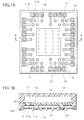
- Fig. 1 is a view describing the semiconductor device of the invention.
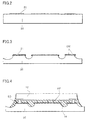
- Fig. 2 is a view describing the method for manufacturing the semiconductor device of the invention.
- Fig. 3 is a view describing the method for manufacturing the semiconductor device of the invention.
- Fig. 4 is a view describing the method for manufacturing the semiconductor device of the invention.
- Fig. 5 is a view describing the method for manufacturing the semiconductor device of the invention.
- Fig. 6 is a view describing the method for manufacturing the semiconductor device of the invention.
- Fig. 7 is a view describing the semiconductor device of the invention.
- Fig. 8 is a view describing the conductive pattern using for the semiconductor device of the invention.
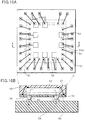
- Fig. 9 is a view describing the semiconductor device shown in Fig. 3.
- Fig. 10 is a view describing the conventional semiconductor device.
- Fig. 1A is a plan view of the semiconductor device
- Fig. 1B is a section view cut with A-A line.
- Fig. 1 the following elements are buried in a insulating resin 10: pads 11A, conductive paths 11B in one body with the pads, external connection electrodes 11C provided at the other ends of the conductive paths 11B in one body with the conductive paths 11B. Further an electrode for radiating 11D provided at one area surrounded by the conductive patterns 11A, 11B, and 11C and a semiconductor chip 12 provided on the electrode for radiating 11D are buried. The semiconductor chip 12 is fixed to said electrode for radiating 11D through under-fill material AF, and is shown with dotted line in Fig. 1A.
- a bonding electrode 13 of the semiconductor chip 12 and the pad 11A are electrically connected through brazing material SD like solder, conductive paste such as Ag paste, and anisotropic conductive resin because the semiconductor chip 12 is mounted in face-down type.
- Side face of said conductive patterns 11A to 11D is etched with non-anisotropy, and has a curved structure because of forming with wet etching so as to generate anchor effect by the curved structure.
- the structure consists of four materials: the semiconductor chip 12, plural conductive patterns 11A to 11C, the electrode for radiation 11D, under-fill material AF, and the insulating resin 10 burying them.
- said under-fill material AF is formed at a trench on and between the conductive patterns 11A to 11D, particularly the insulating resin 10 seals at a state that back face of the under-fill material AF filled in the trench 14 and makes a package.
- Said pads 11A and semiconductor chip 12 are supported by the insulating resin 10 and the under-fill material AF.
- the under-fill material AF comprises insulating material possible to infiltrate through a narrow gap, and material spouting to side face of the semiconductor chip 12 is desirable.
- the under-fill material AF is formed thin at the back face of the semiconductor chip, and the insulating resin 10 may seal the under-fill material AF .
- the under-fill material AF is formed even to the back face of the semiconductor chip 12 and the semiconductor device may be made omitting the insulating resin 10.
- thermosetting resin such as epoxy resin and thermoplastic resin such as polyimide resin and polyphenylenesulfide are used. All kinds of resin are used if they are resins hardening using a die and covering by dipping and painting.
- conductive foil of Cu as main material conductive foil of Al as main material, Fe-Ni alloy, layered product of Cu-Al, or layered product of Al-Cu-Al is used.
- conductive material to etch and to evaporate by laser is desirable.
- conductive material of Cu as main material formed by (expand with pressurizing such as) rolling is desirable.
- the insulating resin 10 and under-fill material AF are filled even in said trench 15 in Fig. 1B, and in Fig. 7, the under-fill material AF is filled even in said trench 15. Therefore the invention has a characteristic to prevent remove of the conductive patterns.
- non-anisotropic etching using dry etching or wet etching for etching, the side faces of pads 11A, the side face of conductive paths 11B, the side face of the external connection electrode 11C, and the electrode for radiation 11D are made into curved structure so as to generate anchor effect. As the result, the structure that the conductive patterns 11A to 11D do not remove from the package is realized.
- the back face of the conductive patterns 11A to 11D expose at the back face of the insulating resin 10.
- the back face of the electrode for radiation 11D may be directly fixed with the electrode on the mounting board omitting the insulating film 16.
- the structure can radiate heat generating from the semiconductor chip 12 to the electrode of the mounting board, can prevent temperature rise of the semiconductor chip 12, and can increase driving current of the semiconductor chip 12 corresponding to the temperature rise.
- the electrode for radiation 11D and the semiconductor chip 12 may be electrically connected.
- the conductive patterns 11A to 11D are supported by insulating resin 10 being sealing resin in the semiconductor device, a supporting board is not need.
- This construction is a characteristic of the invention.
- the conductive path of the conventional semiconductor device is supported by a supporting board (flexible sheet, printed board, or ceramic board), or supported by a lead frame, the construction which is not need originally is added.
- the circuit device comprises necessary minimum components and does not need the supporting board so that the device has a characteristic to be thin, light, and inexpensive because of low material cost.
- the conductive patterns 11A to 11D expose.
- brazing material such as solder for example
- the brazing material can get wet thickly because area of the electrode for radiation 11D is broad. Therefore brazing material of the back face of external connection electrode 11C is not wet at the electrode of the mounting board at fixing on the mounting board, so it is assumed to become bad connection.
- a insulating film 16 is formed at the back face of the semiconductor device 15.
- circles of dotted line shown at the external connection electrodes and electrodes for radiation show the external connection electrodes 11C and electrodes for radiation 11D exposing from the insulating film 16. That is, as the insulating film 16 covers portions except the circles and size of circle portions is substantially same size, thickness of brazing material formed here is substantially same. This is similar as after solder printing and after reflow. This is similar about conductive paste such as Ag, Au, Ag-Pd and so on. By the structure, bad quality of the electrical connection are suppressed.
- An exposing portion 17 of the electrode for radiation 11D may be formed larger than exposing size of the external connection electrode 11C considering radiation of the semiconductor chip.
- all of the external connection electrodes 11C are substantially same size, all area of the external connection electrodes 11C may be exposed, and a part of the back face of the electrode for radiation 11D may be exposed from the insulating film 16 with substantially same size as the external connection electrode 11C.
- the insulating film 16 By providing the insulating film 16, it is possible to extend the conductive path provided at the mounting board to the back face of the semiconductor device. Although the conductive path provided at the mounting board side is generally is arranged going around the fixed area of said semiconductor device, forming said insulating film 16 can arrange without going around. Further as the insulating resin 10 and under-fill material AF are projected out of a surface level of the conductive pattern, a gap is between the conductive path and the conductive pattern formed so as to prevent short.
- the method for manufacturing shows the method for manufacturing of the semiconductor chip shown in Fig. 1, Fig. 2 to Fig. 6 are section views corresponding to A-A line of Fig. 1A.
- a conductive foil 20 is provided as Fig. 2. Thickness thereof is desirably 10 ⁇ m to 300 ⁇ m, here rolled copper foil of 70 ⁇ m is used.
- a conductive film 21 or a photo resist is formed as etching tolerant mask. The pattern is same pattern as the pads 11A, the conductive paths 11B, the external connection electrode 11C, and the electrodes for radiation 11D.
- a conductive film such as Au, Ag, or Ni is formed at a part corresponding to at least pad in the lower layer of the photo resist. This is because surface of Cu is easy to oxidize and bad soldering possibly occurs. These films are able to prevent oxidation of Cu and connection of solder. (Refer Fig. 2 about the above.)
- the conductive foil 20 is half-etched through said conductive film 21 or photo resist. Depth of etching may be thinner than thickness of conductive foil 20. The thinner the depth of etching, forming the finer pattern is possible.
- conductive patterns 11A to 11D appear at surface of the conductive foil 20 in projection shape.
- Cu foil formed by roll and made of Cu as main material is used for the conductive foil 20.
- conductive foil made of Al conductive foil made of Fe-Ni alloy, layered product of Cu-Al, or layered product of Al-Cu-Al may be used.
- layered product of Al-Cu-Al prevents bend appearing by difference of coefficient of thermal expansion.
- Rolled copper foil may be used. This is because growth of crystal of X axis and y axis directions is larger than Z axis and is strong in elasticity.
- stress added to the conductive path 11B becomes large when the conductive path 11B is formed long, resistance to said stress is improved by using the rolled copper foil. (Refer Fig. 3 about the above.)
- the bonding electrode 13 and the pad 11A are arranged so as to face each other with face, and are fixed through brazing material for example.
- the semiconductor chip 12 having solder ball is provided, and paste comprising brazing material is painted on the pad 11A. Viscosity before baking of the paste makes temporary adhesion of the semiconductor chip 12 possible. Setting in an oven with sate of temporary adhesion, the brazing material is melted so that the semiconductor chip 12 and the pad are electrically connected.
- under-fill material AF is formed at a part comprising a definite gap with brazing material.
- the under-fill material AF is a material which is easy to fill into a gap between the semiconductor chip 12 and the conductive pattern, and is formed to side or back face of the semiconductor chip 12 by controlling quantity thereof.
- the under-fill material AF is selected considering adhesiveness of the insulating resin 10 and the conductive pattern.
- the under-fill material AF is provided on a trench 14 between the electrode for radiation 11D and the external connection electrode 11C and a trench 14 between the conductive patterns comprising the pad 11A to the external connection electrode 11C and on them.
- the semiconductor chip is mounted, and height of the semiconductor chip 12 is arranged low as it is mounted with face down type. Therefore thickness of the package described below is made thin. (Refer to Fig. 4 about the above.)
- An insulating resin 10 is formed so as to cover the conductive patterns 11A to 11D formed by half-etching, the semiconductor chip 12.
- the insulating resin both of thermoplasticity and thermosetting property may be used.
- thermosetting resin such as epoxy resin is realized by transfer molding and thermoplastic resin such as liquid crystal polymer and polyphenylenesulfide is realized by injection molding.
- thickness of the insulating resin is adjusted so as to cover 100 ⁇ m upper from the top portion of the semiconductor chip 12.
- the thickness maybe thick or thin considering strength of the semiconductor device.
- the conductive patterns 11A to 11D formed as projection and the semiconductor chip 12 are buried, and the conductive foil 20 of lower part than the projection exposes at the back face. (Refer Fig. 5 about the above.)
- the conductive foil 20 exposing at the back face of the insulating resin 10 is removed and the conductive patterns 11A to 11D are individually separated.
- the back face may be separated removing by etching or grinding by polishing or grinding. Both of them may be used.
- etching or grinding by polishing or grinding Both of them may be used.
- dicing process is added after the separating process.
- the insulating film 16 is formed on the conductive patterns 11A to 11D exposing at the back face separated and is patterned so as to exposes the parts shown in circle of dotted line of Fig. 1A, and after that, it is diced to make the semiconductor device.
- the solder 23 may be formed before or after dicing.
- the above method for manufacturing realizes a light, thin, short, small package where a semiconductor chip buried in insulating material.
- Fig. 7 is an improved semiconductor device of Fig. 1 and the insulating material 10 is omitted. After painting the under-fill material AF so as to form to the back face of the semiconductor chip 12 and solidifying in process of Fig. 4, the device is diced omitting forming the insulating resin 10. In Fig. 7, the back face of the semiconductor chip 12 may be exposed. The plan view of the figure is omitted, as it is same as Fig. 1A.
- a flow-prevention film is formed so that brazing material SD does not flow.
- the flow-prevent film DM at a part of at least the conductive patterns 11A to 11C as shown in Fig. 1B so as to resist flow of solder.
- bad film in wetting ability with solder for example, high polymer film or oxide film formed on Ni film is used.
- FIG. 8 A plan shape of the flow-prevention film is shown in Fig. 8.
- the electrode for radiation is omitted because of the figure.
- the flow-prevention film DM is provided at border of the pad 11A and the conductive path 11B, and the electrical connection means is formed at substantially entire area of the pad 11A.
- the flow-prevention film DM may be formed on an entire area of a conductive path 11B or including the external connection electrode 11C.
- type B the flow-prevention film DM is formed on the pad 11A, and in a part where the electrical connection means is provided, the flow-prevention film DM is removed.
- type C adding to the formed area of type B, the flow-prevention film DM is formed on the conductive path 11B and the external connection electrode 11C.
- the flow-prevention film DM is formed on the pad so as to be a ring shape. Although pat A is shown in rectangle, it may be circle.
- the flow-prevention film DM prevents flow of brazing material such as solder, conductive paste such as Ag paste, and conductive resin, and these electrical connection means consist of bad material in wetting. For example, in case that solder is provided at type D, when the solder melts, the solder is dammed with flow-prevention film DM so as to form fine hemisphere by surface tension.
- passivation film is formed at periphery of the bonding electrode 13 of the semiconductor chip where the solder is attached, only the bonding electrode gets wet. Therefore by connecting the semiconductor chip and the pad through solder, the both are fixed in adductor shape keeping definite height. As size of the exposing portion and height thereof are possible to adjust by volume of solder provided thereon, a definite gap is provided between the semiconductor chip and the conductive pattern. Therefore it is possible to fill washing liquid into the gap. It is possible to fill adhesive low in viscosity such as under-fill material AF. By covering all area except connecting area with the flow-prevention film DM, it is possible to improve adhesiveness with under-fill material AF.
- the pad half-etched to make projection is formed on the conductive foil, it is possible to make the pad fine. Therefore it is possible to make width and gap of the pad so as to form a small package in plan size.
- the device consists of necessary minimum components: the conductive pattern, the semiconductor chip, the connection means, and sealing material, useless material is removed so as to realize thin semiconductor device extremely depressing cost.
- tie bar and hanging lead are not need. Therefore forming and cutting tie bar (hanging lead) is not need at all in the invention.
- Fig. 9 shows the semiconductor device 40.
- Fig. 9A is a plan view of the device, and
- Fig. 9B is a section view cut by A-A line.
- the pad 11A is formed in one body with the conductive path 11B and the external connection electrode 11C in Fig. 1, here the back face of the pad 11A becomes the external connection electrode.
- the pattern exposing from the insulating film 16 is formed in same pattern as said rectangle.
- the grooves 43 are formed so that the electrode for radiation 11D is divided to plural considering adhesion with the under-fill material AF.
- the invention has a reliable construction without a supporting substrate, since the conductive foil where the conductive pattern formed in island shape has certain thickness (or the conductive foil) is buried by the insulating connection means and the insulating resin. AS the electrode for radiation positioning at the back face of the semiconductor chip exposes, radiation of the semiconductor chip is removed. Further as the supporting board is not used, a thin and light package is realized.
- the device consists of necessary minimum components of the conductive pattern, the semiconductor chip, and the insulating resin, and becomes a circuit device useless for resources. Therefore there is not any extra components till completion so as to realize a semiconductor device decreasing cost extremely.
Landscapes
- Structures Or Materials For Encapsulating Or Coating Semiconductor Devices Or Solid State Devices (AREA)
- Encapsulation Of And Coatings For Semiconductor Or Solid State Devices (AREA)
- Cooling Or The Like Of Semiconductors Or Solid State Devices (AREA)
- Wire Bonding (AREA)
- Lead Frames For Integrated Circuits (AREA)
Abstract
Description
Claims (14)
- A semiconductor device comprising:a pad provided facing to a bonding electrode of a semiconductor chip;an electrode for radiation provided at an arranged area of said semiconductor, said semiconductor chip electrically connected to said pad in face down type; andunder-fill material provided on at least a lower face of said semiconductor chip and sealing said semiconductor chip so as to expose a back face of said pad to make in one body.
- A semiconductor device acceding to claim 1, further comprising a insulating resin sealing said semiconductor chip so as to expose a back face of said pad and a back face of said under-fill material to make in one body.
- A semiconductor device according to Claim 2, wherein said under-fill material comes up to a side face of the semiconductor chip and fills in a trench between adjacent said pads and a trench between said pad and said electrode for radiation.
- A semiconductor device according to claim 2, further comprising an external connection electrode provided at a conductive path made in one body with said pad, the external connection electrode surrounds the electrode for radiation,
wherein said insulating resin seals said semiconductor chip so as to expose a back face of said external connection electrode and a back face of said under-fill material to make in one body. - A semiconductor device according to claim 1, further comprising an external connection electrode provided at a conductive path made in one body with said pad, wherein under-fill material is provided on at least a lower face of said semiconductor chip and sealing so as to expose a back face of said external connection electrode and to make in one body.
- A semiconductor device according to Claim 4, wherein said under-fill material comes up to a side face of the semiconductor chip and fills in a trench between adjacent said pads, a trench between adjacent said conductive paths, and a trench between said external connection electrode and said electrode for radiation.
- A semiconductor device according to Claim 1, further comprising a connection means connecting said semiconductor chip and said pad is brazing material, conductive pate, or anisotropic resin.
- A semiconductor device according to Claim 1, wherein side face of said pad comprises a curved structure.
- A semiconductor device according to Claim 4, wherein side face of said pad, the conductive path made in one body with said pad, and the external connection electrode comprise a curved structure.
- A method of manufacturing a semiconductor device comprising the steps of:preparing a conductive foil and half-etching so as to form a conductive pattern in projection;connecting said conductive pattern and a semiconductor chip in face down type;filling under-fill material at least between said semiconductor chip and said conductive foil;providing a insulating resin at said conductive foil so as to seal said semiconductor chip and said conductive pattern; andexposing a back face of said under-fill material and removing a back face of said conductive foil so as to separate as the conductive pattern.
- A method of manufacturing a semiconductor device comprising the steps of:preparing a conductive foil and half-etching so as to form a conductive pattern in projection;connecting said conductive pattern and a semiconductor chip in face down;filling under-fill material at least between said semiconductor chip and said conductive; andexposing a back face of said under-fill material and removing a back face of said conductive foil so as to separate as the conductive pattern.
- A method of manufacturing a semiconductor device according to Claim 10, wherein the device is separated by dicing after separating said conductive pattern.
- A method of manufacturing a semiconductor device according to Claim 10, wherein the conductive pattern becoming a unit is formed in matrix shape at said conductive foil and said semiconductor chip is formed at each unit.
- A method of manufacturing a semiconductor device according to Claim 13, wherein the device is separated between said units by dicing after separating said conductive pattern.
Applications Claiming Priority (2)
| Application Number | Priority Date | Filing Date | Title |
|---|---|---|---|
| JP2000269464 | 2000-09-06 | ||
| JP2000269464A JP3945968B2 (en) | 2000-09-06 | 2000-09-06 | Semiconductor device and manufacturing method thereof |
Publications (2)
| Publication Number | Publication Date |
|---|---|
| EP1187205A2 true EP1187205A2 (en) | 2002-03-13 |
| EP1187205A3 EP1187205A3 (en) | 2004-06-23 |
Family
ID=18756066
Family Applications (1)
| Application Number | Title | Priority Date | Filing Date |
|---|---|---|---|
| EP20010302535 Withdrawn EP1187205A3 (en) | 2000-09-06 | 2001-03-20 | Chip scale package with thermally and electrically conductive pad and manufacturing method thereof |
Country Status (6)
| Country | Link |
|---|---|
| US (1) | US6963126B2 (en) |
| EP (1) | EP1187205A3 (en) |
| JP (1) | JP3945968B2 (en) |
| KR (1) | KR100404061B1 (en) |
| CN (1) | CN1266765C (en) |
| TW (1) | TW511399B (en) |
Cited By (4)
| Publication number | Priority date | Publication date | Assignee | Title |
|---|---|---|---|---|
| WO2003085729A1 (en) * | 2002-04-11 | 2003-10-16 | Koninklijke Philips Electronics N.V. | Method of manufacturing an electronic device |
| WO2003085731A1 (en) | 2002-04-11 | 2003-10-16 | Koninklijke Philips Electronics N.V. | Semiconductor device and method of manufacturing same |
| WO2003085730A1 (en) | 2002-04-11 | 2003-10-16 | Koninklijke Philips Electronics N.V. | Method of manufacturing an electronic device, and electronic device |
| DE102005007643A1 (en) * | 2005-02-19 | 2006-08-31 | Assa Abloy Identification Technology Group Ab | Method and device for contacting semiconductor chips on a metallic substrate |
Families Citing this family (14)
| Publication number | Priority date | Publication date | Assignee | Title |
|---|---|---|---|---|
| US6562671B2 (en) * | 2000-09-22 | 2003-05-13 | Semiconductor Energy Laboratory Co., Ltd. | Semiconductor display device and manufacturing method thereof |
| KR20050029247A (en) * | 2002-08-05 | 2005-03-24 | 코닌클리즈케 필립스 일렉트로닉스 엔.브이. | An electronic product, a body and a method of manufacturing |
| DE10240461A1 (en) * | 2002-08-29 | 2004-03-11 | Infineon Technologies Ag | Universal housing for an electronic component with a semiconductor chip and method for its production |
| JP2004186362A (en) * | 2002-12-03 | 2004-07-02 | Sanyo Electric Co Ltd | Circuit device |
| JP3730644B2 (en) * | 2003-09-11 | 2006-01-05 | ローム株式会社 | Semiconductor device |
| JP2005109225A (en) * | 2003-09-30 | 2005-04-21 | Sanyo Electric Co Ltd | Circuit equipment |
| JP4479209B2 (en) * | 2003-10-10 | 2010-06-09 | パナソニック株式会社 | Electronic circuit device, method for manufacturing the same, and apparatus for manufacturing electronic circuit device |
| JP4446772B2 (en) * | 2004-03-24 | 2010-04-07 | 三洋電機株式会社 | Circuit device and manufacturing method thereof |
| US8070971B2 (en) * | 2004-06-04 | 2011-12-06 | Nxp B.V. | Etch method |
| JP5550102B2 (en) * | 2008-01-17 | 2014-07-16 | 株式会社村田製作所 | Electronic components |
| CN103682043A (en) * | 2013-11-28 | 2014-03-26 | 天津金玛光电有限公司 | Die bonding method for horizontal LED chips and LED light source manufactured by die bonding method |
| CN105161424A (en) * | 2015-07-30 | 2015-12-16 | 南通富士通微电子股份有限公司 | Semiconductor stacked packaging method |
| CN105161425A (en) * | 2015-07-30 | 2015-12-16 | 南通富士通微电子股份有限公司 | Semiconductor stacked packaging method |
| DE102017106055B4 (en) * | 2017-03-21 | 2021-04-08 | Tdk Corporation | Carrier substrate for stress-sensitive component and method of production |
Family Cites Families (17)
| Publication number | Priority date | Publication date | Assignee | Title |
|---|---|---|---|---|
| US5350947A (en) * | 1991-11-12 | 1994-09-27 | Nec Corporation | Film carrier semiconductor device |
| US5677246A (en) * | 1994-11-29 | 1997-10-14 | Kabushiki Kaisha Toshiba | Method of manufacturing semiconductor devices |
| JPH08335653A (en) | 1995-04-07 | 1996-12-17 | Nitto Denko Corp | SEMICONDUCTOR DEVICE, METHOD FOR MANUFACTURING THE SAME, AND TAPE CARRIER FOR SEMICONDUCTOR DEVICE USED IN MANUFACTURING THE SEMICONDUCTOR DEVICE |
| DE19532755C1 (en) | 1995-09-05 | 1997-02-20 | Siemens Ag | Chip module for chip card used as telephone or identification card |
| US5744383A (en) * | 1995-11-17 | 1998-04-28 | Altera Corporation | Integrated circuit package fabrication method |
| JPH09260552A (en) * | 1996-03-22 | 1997-10-03 | Nec Corp | Semiconductor chip mounting structure |
| JPH09312355A (en) * | 1996-05-21 | 1997-12-02 | Shinko Electric Ind Co Ltd | Semiconductor device and manufacturing method thereof |
| JPH10256417A (en) | 1997-03-07 | 1998-09-25 | Citizen Watch Co Ltd | Semiconductor package manufacturing method |
| JPH10335566A (en) | 1997-04-02 | 1998-12-18 | Dainippon Printing Co Ltd | Resin-sealed semiconductor device, circuit member used therefor, and method of manufacturing resin-sealed semiconductor device |
| JPH10303336A (en) | 1997-04-30 | 1998-11-13 | Nec Corp | Resin sealing structure of flip chip type semiconductor element |
| JPH11163024A (en) | 1997-11-28 | 1999-06-18 | Sumitomo Metal Mining Co Ltd | Semiconductor device, lead frame for assembling the same, and method of manufacturing semiconductor device |
| JPH11186326A (en) * | 1997-12-24 | 1999-07-09 | Shinko Electric Ind Co Ltd | Semiconductor device |
| JP3219043B2 (en) * | 1998-01-07 | 2001-10-15 | 日本電気株式会社 | Semiconductor device packaging method and semiconductor device |
| US6410366B1 (en) * | 1998-09-30 | 2002-06-25 | Seiko Epson Corporation | Semiconductor device and manufacturing method thereof, circuit board and electronic equipment |
| JP3395164B2 (en) * | 1998-11-05 | 2003-04-07 | インターナショナル・ビジネス・マシーンズ・コーポレーション | Semiconductor device |
| JP3436159B2 (en) | 1998-11-11 | 2003-08-11 | 松下電器産業株式会社 | Method for manufacturing resin-encapsulated semiconductor device |
| US6383846B1 (en) * | 2000-03-20 | 2002-05-07 | Chi-Chih Shen | Method and apparatus for molding a flip chip semiconductor device |
-
2000
- 2000-09-06 JP JP2000269464A patent/JP3945968B2/en not_active Expired - Lifetime
-
2001
- 2001-02-15 CN CNB011045523A patent/CN1266765C/en not_active Expired - Lifetime
- 2001-02-16 TW TW90103576A patent/TW511399B/en not_active IP Right Cessation
- 2001-02-24 KR KR10-2001-0009508A patent/KR100404061B1/en not_active Expired - Fee Related
- 2001-03-16 US US09/809,923 patent/US6963126B2/en not_active Expired - Lifetime
- 2001-03-20 EP EP20010302535 patent/EP1187205A3/en not_active Withdrawn
Cited By (7)
| Publication number | Priority date | Publication date | Assignee | Title |
|---|---|---|---|---|
| WO2003085729A1 (en) * | 2002-04-11 | 2003-10-16 | Koninklijke Philips Electronics N.V. | Method of manufacturing an electronic device |
| WO2003085731A1 (en) | 2002-04-11 | 2003-10-16 | Koninklijke Philips Electronics N.V. | Semiconductor device and method of manufacturing same |
| WO2003085730A1 (en) | 2002-04-11 | 2003-10-16 | Koninklijke Philips Electronics N.V. | Method of manufacturing an electronic device, and electronic device |
| US7052933B2 (en) | 2002-04-11 | 2006-05-30 | Koninklijke Philips Electronics N.V. | Method of manufacturing an electronic device, and electronic device |
| US7176582B2 (en) | 2002-04-11 | 2007-02-13 | Nxp B.V. | Semiconductor device and method of manufacturing same |
| US7414858B2 (en) | 2002-04-11 | 2008-08-19 | Koninklijke Philips Electronics N.V. | Method of manufacturing an electronic device |
| DE102005007643A1 (en) * | 2005-02-19 | 2006-08-31 | Assa Abloy Identification Technology Group Ab | Method and device for contacting semiconductor chips on a metallic substrate |
Also Published As
| Publication number | Publication date |
|---|---|
| KR20020020170A (en) | 2002-03-14 |
| TW511399B (en) | 2002-11-21 |
| US20020048828A1 (en) | 2002-04-25 |
| EP1187205A3 (en) | 2004-06-23 |
| JP2002083903A (en) | 2002-03-22 |
| JP3945968B2 (en) | 2007-07-18 |
| KR100404061B1 (en) | 2003-11-03 |
| US6963126B2 (en) | 2005-11-08 |
| CN1266765C (en) | 2006-07-26 |
| CN1341963A (en) | 2002-03-27 |
Similar Documents
| Publication | Publication Date | Title |
|---|---|---|
| US6596564B2 (en) | Semiconductor device and method of manufacturing the same | |
| US6791199B2 (en) | Heat radiating semiconductor device | |
| US6963126B2 (en) | Semiconductor device with under-fill material below a surface of a semiconductor chip | |
| US7138296B2 (en) | Board for manufacturing a BGA and method of manufacturing semiconductor device using thereof | |
| US7125798B2 (en) | Circuit device and manufacturing method of circuit device | |
| JP3650001B2 (en) | Semiconductor device and manufacturing method thereof | |
| JP4093818B2 (en) | Manufacturing method of semiconductor device | |
| US20040038471A1 (en) | Semiconductor device and method of manufacturing the same | |
| JP2002076245A (en) | Circuit device and method of manufacturing the same | |
| US6501160B1 (en) | Semiconductor device and a method of manufacturing the same and a mount structure | |
| JP3668101B2 (en) | Semiconductor device | |
| JP2006190987A (en) | Package structure and manufacturing method thereof | |
| JP2001274282A (en) | Semiconductor device | |
| JP2002158315A (en) | Semiconductor device and manufacturing method thereof | |
| JP3963914B2 (en) | Semiconductor device | |
| JP2002083890A (en) | Semiconductor module | |
| JP4863836B2 (en) | Semiconductor device | |
| JP3863816B2 (en) | Circuit equipment | |
| JP2002158310A (en) | Semiconductor device and semiconductor module | |
| JP4115553B2 (en) | Manufacturing method of semiconductor package | |
| JPH0837204A (en) | Semiconductor device and method of manufacturing semiconductor device | |
| JP3778783B2 (en) | Circuit device and manufacturing method thereof | |
| JP3913622B2 (en) | Circuit equipment |
Legal Events
| Date | Code | Title | Description |
|---|---|---|---|
| PUAI | Public reference made under article 153(3) epc to a published international application that has entered the european phase |
Free format text: ORIGINAL CODE: 0009012 |
|
| AK | Designated contracting states |
Kind code of ref document: A2 Designated state(s): AT BE CH CY DE DK ES FI FR GB GR IE IT LI LU MC NL PT SE TR |
|
| AX | Request for extension of the european patent |
Free format text: AL;LT;LV;MK;RO;SI |
|
| PUAL | Search report despatched |
Free format text: ORIGINAL CODE: 0009013 |
|
| AK | Designated contracting states |
Kind code of ref document: A3 Designated state(s): AT BE CH CY DE DK ES FI FR GB GR IE IT LI LU MC NL PT SE TR |
|
| AX | Request for extension of the european patent |
Extension state: AL LT LV MK RO SI |
|
| 17P | Request for examination filed |
Effective date: 20041007 |
|
| 17Q | First examination report despatched |
Effective date: 20041206 |
|
| AKX | Designation fees paid |
Designated state(s): DE FI FR GB NL |
|
| RBV | Designated contracting states (corrected) |
Designated state(s): DE FI FR GB NL |
|
| 17Q | First examination report despatched |
Effective date: 20041206 |
|
| GRAP | Despatch of communication of intention to grant a patent |
Free format text: ORIGINAL CODE: EPIDOSNIGR1 |
|
| STAA | Information on the status of an ep patent application or granted ep patent |
Free format text: STATUS: THE APPLICATION IS DEEMED TO BE WITHDRAWN |
|
| 18D | Application deemed to be withdrawn |
Effective date: 20080917 |