EP1182692A2 - Heat-processing apparatus and method for semiconductor process - Google Patents
Heat-processing apparatus and method for semiconductor process Download PDFInfo
- Publication number
- EP1182692A2 EP1182692A2 EP01203167A EP01203167A EP1182692A2 EP 1182692 A2 EP1182692 A2 EP 1182692A2 EP 01203167 A EP01203167 A EP 01203167A EP 01203167 A EP01203167 A EP 01203167A EP 1182692 A2 EP1182692 A2 EP 1182692A2
- Authority
- EP
- European Patent Office
- Prior art keywords
- zones
- cooling
- process chamber
- cooling gas
- zone
- Prior art date
- Legal status (The legal status is an assumption and is not a legal conclusion. Google has not performed a legal analysis and makes no representation as to the accuracy of the status listed.)
- Granted
Links
Images

Classifications
-
- H—ELECTRICITY
- H10—SEMICONDUCTOR DEVICES; ELECTRIC SOLID-STATE DEVICES NOT OTHERWISE PROVIDED FOR
- H10P—GENERIC PROCESSES OR APPARATUS FOR THE MANUFACTURE OR TREATMENT OF DEVICES COVERED BY CLASS H10
- H10P72/00—Handling or holding of wafers, substrates or devices during manufacture or treatment thereof
- H10P72/04—Apparatus for manufacture or treatment
- H10P72/0431—Apparatus for thermal treatment
- H10P72/0434—Apparatus for thermal treatment mainly by convection
Definitions
- the present invention relates to a heat-processing apparatus and method for a semiconductor process in which a plurality of target substrates are subjected to a heat-process simultaneously, i.e., together at the same time.
- semiconductor process used herein includes various kinds of processes which are performed to manufacture a semiconductor device or a structure having wiring layers, electrodes, and the like to be connected to a semiconductor device, on a target substrate, such as a semiconductor wafer or an LCD substrate, by forming semiconductor layers, insulating layers, and conductive layers in predetermined patterns on the target substrate.
- a vertical heat-processing apparatus In the semiconductor process, a vertical heat-processing apparatus is known as a batch type processing apparatus that applies heat processes, such as oxidation, diffusion, annealing, and CVD, to a number of semiconductor wafers together at the same time.
- the vertical heat-processing apparatus is used such that a number of wafers are arrayed and held with a gap therebetween in a vertical direction in a holder called a wafer boat, and then the holder is loaded into a process chamber of a vertical type. Then, the wafers are subjected to a heat process while they are heated by a heating mechanism disposed around the process chamber.
- the heating mechanism includes a surrounding member formed of a cylindrical heat-insulating body, which forms a heating space around the process chamber.
- a resistance heating wire (heater) is disposed on the inner surface of the surrounding member.
- the heating space comprises a plurality of zones arrayed in a vertical direction, and the heater comprises a plurality of heater segments corresponding to the zones.
- the heater segments can be controlled independently of each other, so that a heat process is performed uniformly over all the zones.
- the heating mechanism is arranged to perform a cooling operation by natural cooling or forcible cooling, which is performed by gas cooling or liquid cooling. As shown in FIG. 5, when the heating mechanism is cooled, the cooling rates of the zones tend to be uneven due to heat discharge and the like. Generally, the cooling rates of the lower and upper zones of the heating space are higher than that of the middle zone. Such unevenness in the cooling rate makes the thermal budgets of wafers in one lot different from each other.
- the cooling rate of the heating space is set when the heat-processing apparatus is first installed, using a method so as to adjust the rate of a zone, which tends to have a higher rate, to be closer to the rate of a zone, which tends to have a lower rate.
- the apparatus is set such that, for example, the heater segments of the lower and upper zones are supplied with a voltage to decrease their cooling rates down to a value as low as the middle zone. In this case, the heat applied to the lower zone warms the middle zone due to convection, radiation, and conduction of the heat, resulting in a decrease in the cooling rate as a whole.
- An object of the present invention is to provide a heat-processing apparatus and method for a semiconductor process, which prevent the cooling rates of the zones of a heating space from differing from each other, and increase the cooling rate of the heating space as a whole.
- Another object of the present invention is to provide a heat-processing apparatus and method for a semiconductor process, which does not entail the troublesome operation for setting the cooling rate of a heating space when the apparatus is installed.
- a heat-processing apparatus for a semiconductor process in which a plurality of target substrates are simultaneously subjected to a heat-process, the apparatus comprising:
- a heat processing method in the apparatus according to the first aspect comprising:
- a vertical heat-processing apparatus for a semiconductor process in which a plurality of target substrates are simultaneously subjected to a heat-process, the apparatus comprising:
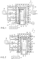
- FIG. 1 is a structural view schematically showing a vertical heat-processing apparatus for processing semiconductor wafers according to an embodiment of the present invention.
- the vertical heat-processing apparatus includes a vertical furnace 1, which functions as, e.g., a high-temperature furnace or diffusion furnace.
- the furnace 1 has a process chamber or process tube 3, and a cylindrical heating mechanism 4 with a liner tube (temperature-unifying tube) 5 interposed between the heating mechanism 4 and the process tube 3.
- a holder such as a boat 2 made of quartz, is placed in the process tube 3.
- the boat 2 holds a number of, e.g., about 150, target substrates, i.e., semiconductor wafers W, such that they are stacked one on the other with a gap therebetween in a vertical direction.
- the heating mechanism 4 is arranged to surround the process tube 3, and to heat the interior of the process tube 3 through the sidewall of the tube 3 to a predetermined temperature of, e.g., from about 600 to 1,200°C.
- the process tube 3 is made of a material, such as quartz, which is heat-resistant and corrosion-resistant, and has a cylindrical shape vertically elongated, with a closed top and an open bottom.
- the lower portion of the process tube 3 is connected to a gas supply line Gi for supplying a process gas or an inactive gas, and an exhaust line Go for exhausting the interior of the process tube 3.
- the gas supply line Gi is connected to a process gas supply section PS.
- the exhaust line Go is connected to a vacuum exhaust section VE including a vacuum pump, a pressure valve, and so forth.
- the process tube 3 may have a double-tube structure formed of inner and outer tubes.
- the bottom end of the process tube 3 is supported by a base plate 6 through an attachment (not shown) disposed below the base plate 6.
- the base plate 6 is made of, e.g., stainless steel, and disposed horizontally in the casing of the vertical heat-processing apparatus.
- the base plate 6 is provided with an opening 7 formed therein, through which the process tube 3 is inserted in a vertical direction.
- a heat-insulating body 8 is attached to the opening 7 around the process tube 3 to prevent the opening 7 from allowing heat to be discharged.
- a lid 9 made of, e.g., stainless steel is disposed below the process tube 3, to be movable up and down by an elevating mechanism (not shown) so as to close and open the bottom opening of the process tube 3.
- a boat 2 is mounted on the lid 9 via an insulating cylinder 10.
- the elevating mechanism is used to transfer the boat 2 into and out of the process tube 3 and to open and close the lid 9.
- the lid 9 is provided with a rotational mechanism (not shown) to rotate the boat 2 along with the insulating cylinder 10, so that the semiconductor wafers W are processed with a high planar uniformity.
- the heating mechanism 4 includes a surrounding member 11, which is formed of a cylindrical heat-insulating body and forms a heating space HS around the process tube 3.
- a heater 12 comprising resistance heating wires is disposed on the inner face of the surrounding member 11 such that the wires meanderingly extend in the angular direction of the member 11 or spirally extend in the longitudinal direction of the member 11.
- the heating space HS consists of a plurality of zones, e.g., five zones Z1 to Z5, arrayed in a vertical direction, while the heater 12 consists of a plurality of heater segments respectively corresponding to the zones.
- the heater segments can be controlled independently of each other, so that a uniform heat process is performed over all the zones.
- the surrounding member 11 is covered with a water-cooling jacket (not shown).
- the heating mechanism 4 is placed on the base plate 6.
- the liner tube 5 is made of, e.g., silicon carbide (SiC).
- the heating space HS is formed as a space substantially closed between the surrounding member 11 and the liner tube 5.
- the liner tube 5 improves uniformity in the heating temperature to the wafers W placed in the process tube 3.
- the liner tube 5 also prevents the wafers W from being contaminated with metals discharged from the resistance heating wires and the like of the heating mechanism 4.
- the liner tube 5 has a cylindrical shape vertically elongated, with a closed top and an open bottom.
- the liner tube 5 surrounds the process tube 3 and is placed on the heat-insulating body 8 of the base plate 6.
- the liner tube 5 may be omitted, such that a heating space HS is formed between the surrounding member 11 and the process tube (process chamber) 3.
- the heating mechanism 4 is provided with a cooling mechanism 13, which forms a flow of cooling gas in each of the zones Z1 to Z5 of the heating space HS to cool the zones Z1 to Z5.
- the cooling mechanism 13 includes supply pipes 15, which respectively supply a cooling gas, such as air (clean air) to the zones Z1 to Z5 to cool them.
- the supply pipes 15 are connected to a common blower (supply blower) 18 for supplying the cooling gas.
- the distal ends of the supply pipes 15 penetrate the sidewall of the surrounding member 11 and come into the respective zones Z1 to Z5 of the heating space HS.
- the cooling mechanism 13 also includes a common exhaust pipe 20 connected to a blower (exhaust blower) 19 for exhausting the cooling gas from the heating space HS.
- the supply pipes 15 are respectively provided with valves 16 to adjust supply rates of the cooling gas into the zones Z1 to Z5.
- Each of the valves 16 is formed of, e.g., a valve of the type driven by an actuator, whose opening degree is controlled by a controller 17.
- Temperature sensors 14 are arranged to detect temperatures respectively representing the zones Z1 to Z5 of the heating space HS.
- the temperature sensors 14 consist of, e.g., thermocouples, disposed between the process tube 3 and the liner tube 5 to respectively correspond to the zones Z1 to Z5.
- Each of the temperature sensors 14 may be inserted in and covered with a protection tube made of quartz.
- the controller 17 is set to recognize as a reference value the cooling rate of a zone that has the highest cooling rate, when it controls the flow of the cooling gas.
- the reference value may be a fixed value, which has been obtained by experiment and the like in advance, and inputted into the controller 17. Instead, the reference value may be a non-fixed value, which is calculated at each time by the controller 17 on the basis of temperatures detected by the temperature sensors 14 during a cooling operation.
- the controller 17 controls the opening degrees of the valves 16 of the supply pipes 15, on the basis of the temperatures corresponding to the zones Z1 to Z5, which are detected by the temperature sensors 14, so that the cooling rate of the heating space HS as a whole is adjusted to be the reference value. More specifically, the controller 17 controls, on the basis of the detected temperatures, the supply rate of cooling air to a zone having a lower cooling rate, such as the middle zones Z3, to be higher than that to a zone having the highest cooling rate, such as the lower zones Z5, so that the lower cooling rate is adjusted to be closer to, i.e., approximate, the highest cooling rate.
- the controller 17 controls the cooling mechanism 13 such that the flow velocity of the cooling gas in a first zone having a lower cooling rate becomes higher than the flow velocity of the cooling gas in a second zone having a higher cooling rate, thereby adjusting the cooling rate of the first zone to be closer to the cooling rate of the second zone.
- the boat 2 which has been loaded with wafers W, is placed on the insulating cylinder 10 supported by the lid 9 at a loading area below the heating mechanism 4. Then, the lid 9 is moved up by the elevating mechanism, so that the boat 2 is inserted into the process tube 3 through the bottom opening, which is then airtightly closed by the lid 9. Then, while the process tube 3 is exhausted, the wafers W on the boat 2 are heated up to a predetermined process temperature by the heating mechanism 4. Then, while the process tube 3 is exhausted, a predetermined process gas is supplied into the process tube 3 to subject the wafers W to a predetermined heat process, such as a diffusion process.
- a predetermined process gas is supplied into the process tube 3 to subject the wafers W to a predetermined heat process, such as a diffusion process.
- the heater 12 of the heating mechanism 4 is first turned off. Then, the blower 18 is operated to supply air used as a cooling gas through the supply pipes 15 into the heating space HS, so as to forcibly cool the interior of the heating space HS.
- the temperature sensors 14 detect temperatures representing the zones Z1 to Z5.
- the controller 17 controls, on the basis of the detected temperatures, the supply rate of cooling air to a zone having a lower cooling rate, such as the middle zones Z3, to be higher than that to a zone having the highest cooling rate, such as the lower zones Z5, so that the lower cooling rate is adjusted to be closer to the highest cooling rate.
- the vertical heat-processing apparatus shown in FIG. 1 can automatically control the cooling rates of the zones Z1 to Z5 to be uniform under the control of the controller 17.
- the cooling rate of the heating space HS can be higher as a whole to improve the thermodynamics.
- FIG. 2 is a structural view schematically showing a vertical heat-processing apparatus for processing semiconductor wafers according to another embodiment of the present invention.
- This vertical heat-processing apparatus includes a heating space HS, which comprises zones Z1 to Z5 separated from each other by partitions 21 made of, e.g., quartz.
- the zones Z1 to Z5 are respectively provided with exhaust pipes 22 connected thereto, for exhausting a cooling gas independently of each other.
- the vertical heat-processing apparatus shown in FIG. 2 can provide the same effect as the vertical heat-processing apparatus shown in FIG. 1. Furthermore, since the heating space HS is divided into the zones Z1 to Z5 by the partitions 21, the zones Z1 to Z5 can be cooled independently of each other. As in this embodiment, where the heating space HS is partitioned into the zones Z1 to Z5, it is possible to form a flow of the cooling gas only in a zone having a lower cooling rate so as to solve a temperature difference between the zones, in the case of not only the forcible cooling, but also natural cooling.
- FIG. 3 is a structural view schematically showing a vertical heat-processing apparatus for processing semiconductor wafers according to still another embodiment of the present invention.
- This vertical heat-processing apparatus includes a heating space HS, which comprises zones Z1 to Z5 separated from each other by partitions 21 made of, e.g., quartz.
- the zones Z1 to Z5 are respectively provided with supply pipes 27 connected thereto, for supplying a cooling gas independently of each other, and exhaust pipes 23 connected thereto, for exhausting the cooling gas independently of each other.
- the exhaust pipes 23 are connected to a common blower (exhaust blower) 25.
- the exhaust pipes 23 are respectively provided with valves 24 to adjust exhaust rates of the cooling gas from the zones Z1 to Z5.
- Each of the valves 24 is formed of, e.g., a valve of the type driven by an actuator, whose opening degree is controlled by a controller 17.
- Temperature sensors 14 are arranged to detect temperatures respectively representing the zones Z1 to Z5 of the heating space HS.
- the controller 17 controls the opening degrees of the valves 24 of the exhaust pipes 23, on the basis of the temperatures corresponding to the zones Z1 to Z5, which are detected by the temperature sensors 14, so that the cooling rate of the heating space HS as a whole is adjusted to be a reference value corresponding to the highest cooling rate. More specifically, the controller 17 controls, on the basis of the detected temperatures, the exhaust rate of cooling air from a zone having a lower cooling rate, such as the middle zones Z3, to be higher than that from a zone having the highest cooling rate, such as the lower zones Z5, so that the lower cooling rate is adjusted to be closer to, i.e., approximate, the highest cooling rate.
- the controller 17 controls the cooling mechanism 13 such that the flow velocity of the cooling gas in a first zone having a lower cooling rate becomes higher than the flow velocity of the cooling gas in a second zone having a higher cooling rate, thereby adjusting the cooling rate of the first zone to be closer to the cooling rate of the second zone.
- the vertical heat-processing apparatus shown in FIG. 3 can automatically control the cooling rates of the zones Z1 to Z5 to be uniform under the control of the controller 17.
- the cooling rate of the heating space HS can be higher as a whole to improve the thermodynamics.
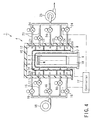
- FIG. 4 is a structural view schematically showing a vertical heat-processing apparatus for processing semiconductor wafers according to still another embodiment of the present invention.
- This vertical heat-processing apparatus has a structure combining the features shown in FIG. 2 and the features shown in FIG. 3 with each other. More specifically, the vertical heat-processing apparatus includes a heating space HS, which comprises zones Z1 to Z5 separated from each other by partitions 21 made of, e.g., quartz.
- the zones Z1 to Z5 are respectively provided with supply pipes 15 connected thereto, for supplying a cooling gas independently of each other, and exhaust pipes 23 connected thereto, for exhausting the cooling gas independently of each other.
- the supply pipes 15 are connected to a common blower (supply blower) 18, and the exhaust pipes 23 are connected to a common blower (exhaust blower) 25.
- the supply pipes 15 are respectively provided with valves 16 to adjust supply rates of the cooling gas into the zones Z1 to Z5.
- the exhaust pipes 23 are respectively provided with valves 24 to adjust exhaust rates of the cooling gas from the zones Z1 to Z5.
- the controller 17 controls the opening degrees of the valves 16 of the supply pipes 15 and the opening degrees of the valves 24 of the exhaust pipes 23, on the basis of the temperatures corresponding to the zones Z1 to Z5, which are detected by the temperature sensors 14, so that the cooling rate of the heating space HS as a whole is adjusted to be a reference value corresponding to the highest cooling rate.
- the vertical heat-processing apparatus shown in FIG. 4 can more reliably achieve the advantages described with reference to the vertical heat-processing apparatuses shown in FIGS. 1 to 3, i.e., to prevent the cooling rates of the zones Z1 to Z5 from being uneven, and to control the cooling rate of the heating space HS to be higher as a whole.
- the liner tube 5 may be omitted, wherein the heating space HS is formed between the surrounding member 11 and the process tube (process chamber) 3.
- a manifold made of a metal, such as stainless steel, and provided with a gas supply line and an exhaust line may be airtightly attached to the bottom of the process tube 3.
- the present invention may be applied to a low-temperature furnace, such as a CVD furnace.
- the present invention may also be applied to a horizontal heat-processing apparatus in place of the vertical heat-processing apparatus.
- the present invention may be applied to a target substrate other than a semiconductor wafer, such as an LCD substrate, or a glass substrate.
Landscapes
- Chemical Vapour Deposition (AREA)
- Muffle Furnaces And Rotary Kilns (AREA)
Abstract
Description
- The present invention relates to a heat-processing apparatus and method for a semiconductor process in which a plurality of target substrates are subjected to a heat-process simultaneously, i.e., together at the same time. The term "semiconductor process" used herein includes various kinds of processes which are performed to manufacture a semiconductor device or a structure having wiring layers, electrodes, and the like to be connected to a semiconductor device, on a target substrate, such as a semiconductor wafer or an LCD substrate, by forming semiconductor layers, insulating layers, and conductive layers in predetermined patterns on the target substrate.
- In the semiconductor process, a vertical heat-processing apparatus is known as a batch type processing apparatus that applies heat processes, such as oxidation, diffusion, annealing, and CVD, to a number of semiconductor wafers together at the same time. The vertical heat-processing apparatus is used such that a number of wafers are arrayed and held with a gap therebetween in a vertical direction in a holder called a wafer boat, and then the holder is loaded into a process chamber of a vertical type. Then, the wafers are subjected to a heat process while they are heated by a heating mechanism disposed around the process chamber.
- The heating mechanism includes a surrounding member formed of a cylindrical heat-insulating body, which forms a heating space around the process chamber. A resistance heating wire (heater) is disposed on the inner surface of the surrounding member. Preferably, the heating space comprises a plurality of zones arrayed in a vertical direction, and the heater comprises a plurality of heater segments corresponding to the zones. The heater segments can be controlled independently of each other, so that a heat process is performed uniformly over all the zones.
- The heating mechanism is arranged to perform a cooling operation by natural cooling or forcible cooling, which is performed by gas cooling or liquid cooling. As shown in FIG. 5, when the heating mechanism is cooled, the cooling rates of the zones tend to be uneven due to heat discharge and the like. Generally, the cooling rates of the lower and upper zones of the heating space are higher than that of the middle zone. Such unevenness in the cooling rate makes the thermal budgets of wafers in one lot different from each other.
- The cooling rate of the heating space is set when the heat-processing apparatus is first installed, using a method so as to adjust the rate of a zone, which tends to have a higher rate, to be closer to the rate of a zone, which tends to have a lower rate. In an apparatus of the natural cooling type, the apparatus is set such that, for example, the heater segments of the lower and upper zones are supplied with a voltage to decrease their cooling rates down to a value as low as the middle zone. In this case, the heat applied to the lower zone warms the middle zone due to convection, radiation, and conduction of the heat, resulting in a decrease in the cooling rate as a whole.
- On the other hand, when an apparatus of the forcible cooling type is installed, supply rates of a cooling gas to the zones are adjusted in order to set the cooling rate of the heating space such that the cooling rate of the middle zone becomes almost the same as those of the lower and upper zones. In this case, it is necessary to perform a troublesome operation of repeatedly adjusting manual valves on air supply pipes while confirming the cooling rates of the zones.
- An object of the present invention is to provide a heat-processing apparatus and method for a semiconductor process, which prevent the cooling rates of the zones of a heating space from differing from each other, and increase the cooling rate of the heating space as a whole.
- Another object of the present invention is to provide a heat-processing apparatus and method for a semiconductor process, which does not entail the troublesome operation for setting the cooling rate of a heating space when the apparatus is installed.
- According to a first aspect of the present invention, there is provided a heat-processing apparatus for a semiconductor process in which a plurality of target substrates are simultaneously subjected to a heat-process, the apparatus comprising:
- a process chamber, which accommodates the target substrates;
- a holder, which holds the target substrates with a gap therebetween in the process chamber;
- a heater disposed around the process chamber, which heats an interior of the process chamber through a sidewall of the process chamber;
- a surrounding member, which surrounds the process chamber and the heater, and forms a heating space around the process chamber, the heating space comprising a plurality of zones juxtaposed in a direction in which the target substrates are arrayed;
- a plurality of the temperature sensors, which detect temperatures respectively representing the zones;
- a cooling mechanism, which forms flows of a cooling gas respectively in the zones, and cools the zones; and
- a controller, which controls the cooling mechanism on the basis of temperatures detected by the temperature sensors when the process chamber is cooled, such that a flow velocity of the cooling gas in a first zone having a lower cooling rate becomes higher than a flow velocity of the cooling gas in a second zone having a higher cooling rate used as a reference, thereby adjusting the cooling rate of the first zone to be closer to the cooling rate of the second zone.
-
- According to a second aspect of the present invention, there is provided a heat processing method in the apparatus according to the first aspect, comprising:
- subjecting the target substrates to a heat process, in which the target substrates are held by the holder in the process chamber, and heated by the heater;
- performing, after the heat process, a cooling operation to cool the process chamber, in which the controller controls the cooling mechanism on the basis of temperatures detected by the temperature sensors, such that a flow velocity of the cooling gas in a first zone having a lower cooling rate becomes higher than a flow velocity of the cooling gas in a second zone having a higher cooling rate used as a reference, thereby adjusting the cooling rate of the first zone to be closer to the cooling rate of the second zone.
-
- According to a third aspect of the present invention, there is provided a vertical heat-processing apparatus for a semiconductor process in which a plurality of target substrates are simultaneously subjected to a heat-process, the apparatus comprising:
- a process chamber, which accommodates the target substrates;
- a supply section, which supplies the process gas into the process chamber;
- an exhaust section, which exhausts the process chamber;
- a holder, which holds the target substrates in the process chamber such that they are stacked one on the other with a gap therebetween in a vertical direction;
- a heater disposed around the process chamber, which heats an interior of the process chamber through a sidewall of the process chamber;
- a surrounding member, which surrounds the process chamber and the heater, and forms a heating space around the process chamber, the heating space comprising a plurality of zones juxtaposed in a vertical direction;
- a plurality of the temperature sensors, which detect temperatures respectively representing the zones;
- a cooling mechanism, which forms flows of a cooling gas respectively in the zones, and cools the zones, the cooling mechanism comprising a plurality of supply pipes, which respectively supply the cooling gas to the zones to cool the zones, a plurality of valves respectively arranged on the supply pipes to adjust supply rates of the cooling gas to the zones, and an exhaust pipe, which exhausts the cooling gas from the zones; and
- a controller, which adjusts opening degrees of the valves on the basis of temperatures detected by the temperature sensors when the process chamber is cooled, such that a flow velocity of the cooling gas in a first zone having a lower cooling rate becomes higher than a flow velocity of the cooling gas in a second zone having a higher cooling rate used as a reference, thereby adjusting the cooling rate of the first zone to be closer to the cooling rate of the second zone.
-
- This summary of the invention does not necessarily describe all necessary features so that the invention may also be a sub-combination of these described features.
- The invention can be more fully understood from the following detailed description when taken in conjunction with the accompanying drawings, in which:
- FIG. 1 is a structural view schematically showing a vertical heat-processing apparatus for processing semiconductor wafers according to an embodiment of the present invention;
- FIG. 2 is a structural view schematically showing a vertical heat-processing apparatus for processing semiconductor wafers according to another embodiment of the present invention;
- FIG. 3 is a structural view schematically showing a vertical heat-processing apparatus for processing semiconductor wafers according to still another embodiment of the present invention;
- FIG. 4 is a structural view schematically showing a vertical heat-processing apparatus for processing semiconductor wafers according to still another embodiment of the present invention; and
- FIG. 5 is a graph showing the cooling rate of a heating space in a vertical heat-processing apparatus.
-
- Embodiments of the present invention will be described hereinafter with reference to the accompanying drawings. In the following description, the constituent elements having substantially the same function and arrangement are denoted by the same reference numerals, and a repetitive description will be made only when necessary.
- FIG. 1 is a structural view schematically showing a vertical heat-processing apparatus for processing semiconductor wafers according to an embodiment of the present invention. The vertical heat-processing apparatus includes a vertical furnace 1, which functions as, e.g., a high-temperature furnace or diffusion furnace. The furnace 1 has a process chamber or
process tube 3, and acylindrical heating mechanism 4 with a liner tube (temperature-unifying tube) 5 interposed between theheating mechanism 4 and theprocess tube 3. A holder, such as aboat 2 made of quartz, is placed in theprocess tube 3. Theboat 2 holds a number of, e.g., about 150, target substrates, i.e., semiconductor wafers W, such that they are stacked one on the other with a gap therebetween in a vertical direction. Theheating mechanism 4 is arranged to surround theprocess tube 3, and to heat the interior of theprocess tube 3 through the sidewall of thetube 3 to a predetermined temperature of, e.g., from about 600 to 1,200°C. - The
process tube 3 is made of a material, such as quartz, which is heat-resistant and corrosion-resistant, and has a cylindrical shape vertically elongated, with a closed top and an open bottom. The lower portion of theprocess tube 3 is connected to a gas supply line Gi for supplying a process gas or an inactive gas, and an exhaust line Go for exhausting the interior of theprocess tube 3. The gas supply line Gi is connected to a process gas supply section PS. The exhaust line Go is connected to a vacuum exhaust section VE including a vacuum pump, a pressure valve, and so forth. Theprocess tube 3 may have a double-tube structure formed of inner and outer tubes. - The bottom end of the
process tube 3 is supported by abase plate 6 through an attachment (not shown) disposed below thebase plate 6. Thebase plate 6 is made of, e.g., stainless steel, and disposed horizontally in the casing of the vertical heat-processing apparatus. Thebase plate 6 is provided with anopening 7 formed therein, through which theprocess tube 3 is inserted in a vertical direction. A heat-insulatingbody 8 is attached to the opening 7 around theprocess tube 3 to prevent theopening 7 from allowing heat to be discharged. - A
lid 9 made of, e.g., stainless steel is disposed below theprocess tube 3, to be movable up and down by an elevating mechanism (not shown) so as to close and open the bottom opening of theprocess tube 3. Aboat 2 is mounted on thelid 9 via an insulatingcylinder 10. The elevating mechanism is used to transfer theboat 2 into and out of theprocess tube 3 and to open and close thelid 9. Thelid 9 is provided with a rotational mechanism (not shown) to rotate theboat 2 along with the insulatingcylinder 10, so that the semiconductor wafers W are processed with a high planar uniformity. - The
heating mechanism 4 includes a surroundingmember 11, which is formed of a cylindrical heat-insulating body and forms a heating space HS around theprocess tube 3. Aheater 12 comprising resistance heating wires is disposed on the inner face of the surroundingmember 11 such that the wires meanderingly extend in the angular direction of themember 11 or spirally extend in the longitudinal direction of themember 11. The heating space HS consists of a plurality of zones, e.g., five zones Z1 to Z5, arrayed in a vertical direction, while theheater 12 consists of a plurality of heater segments respectively corresponding to the zones. The heater segments can be controlled independently of each other, so that a uniform heat process is performed over all the zones. The surroundingmember 11 is covered with a water-cooling jacket (not shown). Theheating mechanism 4 is placed on thebase plate 6. - The
liner tube 5 is made of, e.g., silicon carbide (SiC). The heating space HS is formed as a space substantially closed between the surroundingmember 11 and theliner tube 5. Theliner tube 5 improves uniformity in the heating temperature to the wafers W placed in theprocess tube 3. Theliner tube 5 also prevents the wafers W from being contaminated with metals discharged from the resistance heating wires and the like of theheating mechanism 4. Theliner tube 5 has a cylindrical shape vertically elongated, with a closed top and an open bottom. Theliner tube 5 surrounds theprocess tube 3 and is placed on the heat-insulatingbody 8 of thebase plate 6. Theliner tube 5 may be omitted, such that a heating space HS is formed between the surroundingmember 11 and the process tube (process chamber) 3. - The
heating mechanism 4 is provided with acooling mechanism 13, which forms a flow of cooling gas in each of the zones Z1 to Z5 of the heating space HS to cool the zones Z1 to Z5. Thecooling mechanism 13 includessupply pipes 15, which respectively supply a cooling gas, such as air (clean air) to the zones Z1 to Z5 to cool them. Thesupply pipes 15 are connected to a common blower (supply blower) 18 for supplying the cooling gas. The distal ends of thesupply pipes 15 penetrate the sidewall of the surroundingmember 11 and come into the respective zones Z1 to Z5 of the heating space HS. Thecooling mechanism 13 also includes acommon exhaust pipe 20 connected to a blower (exhaust blower) 19 for exhausting the cooling gas from the heating space HS. - The
supply pipes 15 are respectively provided withvalves 16 to adjust supply rates of the cooling gas into the zones Z1 to Z5. Each of thevalves 16 is formed of, e.g., a valve of the type driven by an actuator, whose opening degree is controlled by acontroller 17.Temperature sensors 14 are arranged to detect temperatures respectively representing the zones Z1 to Z5 of the heating space HS. Thetemperature sensors 14 consist of, e.g., thermocouples, disposed between theprocess tube 3 and theliner tube 5 to respectively correspond to the zones Z1 to Z5. Each of thetemperature sensors 14 may be inserted in and covered with a protection tube made of quartz. - The
controller 17 is set to recognize as a reference value the cooling rate of a zone that has the highest cooling rate, when it controls the flow of the cooling gas. The reference value may be a fixed value, which has been obtained by experiment and the like in advance, and inputted into thecontroller 17. Instead, the reference value may be a non-fixed value, which is calculated at each time by thecontroller 17 on the basis of temperatures detected by thetemperature sensors 14 during a cooling operation. - The
controller 17 controls the opening degrees of thevalves 16 of thesupply pipes 15, on the basis of the temperatures corresponding to the zones Z1 to Z5, which are detected by thetemperature sensors 14, so that the cooling rate of the heating space HS as a whole is adjusted to be the reference value. More specifically, thecontroller 17 controls, on the basis of the detected temperatures, the supply rate of cooling air to a zone having a lower cooling rate, such as the middle zones Z3, to be higher than that to a zone having the highest cooling rate, such as the lower zones Z5, so that the lower cooling rate is adjusted to be closer to, i.e., approximate, the highest cooling rate. In other words, thecontroller 17 controls thecooling mechanism 13 such that the flow velocity of the cooling gas in a first zone having a lower cooling rate becomes higher than the flow velocity of the cooling gas in a second zone having a higher cooling rate, thereby adjusting the cooling rate of the first zone to be closer to the cooling rate of the second zone. - An explanation will be given of a heat processing method in the vertical heat-processing apparatus shown in FIG. 1.
- First, the
boat 2, which has been loaded with wafers W, is placed on the insulatingcylinder 10 supported by thelid 9 at a loading area below theheating mechanism 4. Then, thelid 9 is moved up by the elevating mechanism, so that theboat 2 is inserted into theprocess tube 3 through the bottom opening, which is then airtightly closed by thelid 9. Then, while theprocess tube 3 is exhausted, the wafers W on theboat 2 are heated up to a predetermined process temperature by theheating mechanism 4. Then, while theprocess tube 3 is exhausted, a predetermined process gas is supplied into theprocess tube 3 to subject the wafers W to a predetermined heat process, such as a diffusion process. - After the heat process ends, the
heater 12 of theheating mechanism 4 is first turned off. Then, theblower 18 is operated to supply air used as a cooling gas through thesupply pipes 15 into the heating space HS, so as to forcibly cool the interior of the heating space HS. At this time, thetemperature sensors 14 detect temperatures representing the zones Z1 to Z5. Thecontroller 17 controls, on the basis of the detected temperatures, the supply rate of cooling air to a zone having a lower cooling rate, such as the middle zones Z3, to be higher than that to a zone having the highest cooling rate, such as the lower zones Z5, so that the lower cooling rate is adjusted to be closer to the highest cooling rate. As a result, it is possible to prevent the cooling rates of the zones Z1 to Z5 from being uneven, and also to cause the cooling rates to be higher as a whole. Furthermore, as this method allows a flexible control oriented toward a decrease in temperature, the thermodynamics of the furnace 1 is improved. - Accordingly, the vertical heat-processing apparatus shown in FIG. 1 can automatically control the cooling rates of the zones Z1 to Z5 to be uniform under the control of the
controller 17. In addition, the cooling rate of the heating space HS can be higher as a whole to improve the thermodynamics. - FIG. 2 is a structural view schematically showing a vertical heat-processing apparatus for processing semiconductor wafers according to another embodiment of the present invention. This vertical heat-processing apparatus includes a heating space HS, which comprises zones Z1 to Z5 separated from each other by
partitions 21 made of, e.g., quartz. The zones Z1 to Z5 are respectively provided withexhaust pipes 22 connected thereto, for exhausting a cooling gas independently of each other. - The vertical heat-processing apparatus shown in FIG. 2 can provide the same effect as the vertical heat-processing apparatus shown in FIG. 1. Furthermore, since the heating space HS is divided into the zones Z1 to Z5 by the
partitions 21, the zones Z1 to Z5 can be cooled independently of each other. As in this embodiment, where the heating space HS is partitioned into the zones Z1 to Z5, it is possible to form a flow of the cooling gas only in a zone having a lower cooling rate so as to solve a temperature difference between the zones, in the case of not only the forcible cooling, but also natural cooling. - FIG. 3 is a structural view schematically showing a vertical heat-processing apparatus for processing semiconductor wafers according to still another embodiment of the present invention. This vertical heat-processing apparatus includes a heating space HS, which comprises zones Z1 to Z5 separated from each other by
partitions 21 made of, e.g., quartz. The zones Z1 to Z5 are respectively provided withsupply pipes 27 connected thereto, for supplying a cooling gas independently of each other, andexhaust pipes 23 connected thereto, for exhausting the cooling gas independently of each other. Theexhaust pipes 23 are connected to a common blower (exhaust blower) 25. - The
exhaust pipes 23 are respectively provided withvalves 24 to adjust exhaust rates of the cooling gas from the zones Z1 to Z5. Each of thevalves 24 is formed of, e.g., a valve of the type driven by an actuator, whose opening degree is controlled by acontroller 17.Temperature sensors 14 are arranged to detect temperatures respectively representing the zones Z1 to Z5 of the heating space HS. - The
controller 17 controls the opening degrees of thevalves 24 of theexhaust pipes 23, on the basis of the temperatures corresponding to the zones Z1 to Z5, which are detected by thetemperature sensors 14, so that the cooling rate of the heating space HS as a whole is adjusted to be a reference value corresponding to the highest cooling rate. More specifically, thecontroller 17 controls, on the basis of the detected temperatures, the exhaust rate of cooling air from a zone having a lower cooling rate, such as the middle zones Z3, to be higher than that from a zone having the highest cooling rate, such as the lower zones Z5, so that the lower cooling rate is adjusted to be closer to, i.e., approximate, the highest cooling rate. In other words, thecontroller 17 controls thecooling mechanism 13 such that the flow velocity of the cooling gas in a first zone having a lower cooling rate becomes higher than the flow velocity of the cooling gas in a second zone having a higher cooling rate, thereby adjusting the cooling rate of the first zone to be closer to the cooling rate of the second zone. - Accordingly, the vertical heat-processing apparatus shown in FIG. 3 can automatically control the cooling rates of the zones Z1 to Z5 to be uniform under the control of the
controller 17. In addition, the cooling rate of the heating space HS can be higher as a whole to improve the thermodynamics. - FIG. 4 is a structural view schematically showing a vertical heat-processing apparatus for processing semiconductor wafers according to still another embodiment of the present invention. This vertical heat-processing apparatus has a structure combining the features shown in FIG. 2 and the features shown in FIG. 3 with each other. More specifically, the vertical heat-processing apparatus includes a heating space HS, which comprises zones Z1 to Z5 separated from each other by
partitions 21 made of, e.g., quartz. The zones Z1 to Z5 are respectively provided withsupply pipes 15 connected thereto, for supplying a cooling gas independently of each other, andexhaust pipes 23 connected thereto, for exhausting the cooling gas independently of each other. Thesupply pipes 15 are connected to a common blower (supply blower) 18, and theexhaust pipes 23 are connected to a common blower (exhaust blower) 25. - The
supply pipes 15 are respectively provided withvalves 16 to adjust supply rates of the cooling gas into the zones Z1 to Z5. Theexhaust pipes 23 are respectively provided withvalves 24 to adjust exhaust rates of the cooling gas from the zones Z1 to Z5. Thecontroller 17 controls the opening degrees of thevalves 16 of thesupply pipes 15 and the opening degrees of thevalves 24 of theexhaust pipes 23, on the basis of the temperatures corresponding to the zones Z1 to Z5, which are detected by thetemperature sensors 14, so that the cooling rate of the heating space HS as a whole is adjusted to be a reference value corresponding to the highest cooling rate. - Accordingly, the vertical heat-processing apparatus shown in FIG. 4 can more reliably achieve the advantages described with reference to the vertical heat-processing apparatuses shown in FIGS. 1 to 3, i.e., to prevent the cooling rates of the zones Z1 to Z5 from being uneven, and to control the cooling rate of the heating space HS to be higher as a whole.
- In all the embodiments, the
liner tube 5 may be omitted, wherein the heating space HS is formed between the surroundingmember 11 and the process tube (process chamber) 3. A manifold made of a metal, such as stainless steel, and provided with a gas supply line and an exhaust line may be airtightly attached to the bottom of theprocess tube 3. - The present invention may be applied to a low-temperature furnace, such as a CVD furnace. The present invention may also be applied to a horizontal heat-processing apparatus in place of the vertical heat-processing apparatus. Furthermore, the present invention may be applied to a target substrate other than a semiconductor wafer, such as an LCD substrate, or a glass substrate.
Claims (20)
- A heat-processing apparatus for a semiconductor process in which a plurality of target substrates (W) are simultaneously subjected to a heat-process, the apparatus characterized by comprising:a process chamber (3), which accommodates the target substrates;a holder (2), which holds the target substrates with a gap therebetween in the process chamber;a heater (12) disposed around the process chamber, which heats an interior of the process chamber through a sidewall of the process chamber;a surrounding member (11), which surrounds the process chamber and the heater, and forms a heating space (HS) around the process chamber, the heating space comprising a plurality of zones (Z1 - Z5) juxtaposed in a direction in which the target substrates are arrayed;a plurality of the temperature sensors (14), which detect temperatures respectively representing the zones;a cooling mechanism (13), which forms flows of a cooling gas respectively in the zones, and cools the zones; anda controller (17), which controls the cooling mechanism on the basis of temperatures detected by the temperature sensors when the process chamber is cooled, such that a flow velocity of the cooling gas in a first zone having a lower cooling rate becomes higher than a flow velocity of the cooling gas in a second zone having a higher cooling rate used as a reference, thereby adjusting the cooling rate of the first zone to be closer to the cooling rate of the second zone.
- The apparatus according to claim 1, characterized in that the cooling mechanism (13) comprises a plurality of supply pipes (15), which respectively supply the cooling gas to the zones (Z1 - Z5) to cool the zones, and a plurality of valves (16) respectively arranged on the supply pipes to adjust supply rates of the cooling gas to the zones, and the controller (17) adjusts opening degrees of the valves to control flow velocities of the cooling gas in the zones.
- The apparatus according to claim 2, characterized in that the supply pipes (15) are connected to a common blower (18), which supplies the cooling gas to the supply pipes.
- The apparatus according to claim 2, characterized in that the cooling mechanism (13) comprises a common exhaust pipe (20), which exhausts the cooling gas from all the zones (Z1 - Z5).
- The apparatus according to claim 2, characterized in that the cooling mechanism (13) comprises a plurality of exhaust pipes (22), which respectively exhaust the cooling gas from the zones (Z1 - Z5).
- The apparatus according to claim 1, characterized in that the cooling mechanism (13) comprises a supply pipe (27), which supplies the cooling gas to the zones (Z1 - Z5) to cool the zones, a plurality of exhaust pipes (23), which respectively exhaust the cooling gas from the zones, and a plurality of valves (24) respectively arranged on the exhaust pipes to adjust exhaust rates of the cooling gas from the zones, and the controller (17) adjusts opening degrees of the valves to control flow velocities of the cooling gas in the zones.
- The apparatus according to claim 6, characterized in that the exhaust pipes (23) are connected to a common blower (25), which exhausts the cooling gas from the exhaust pipes.
- The apparatus according to claim 6, characterized in that the cooling mechanism (13) comprises a plurality of supply pipes (27), which respectively supply the cooling gas to the zones to cool the zones (Z1 - Z5).
- The apparatus according to claim 1, characterized in that the zones (Z1 - Z5) are separated from each other by partitions (21) disposed in the heating space (HS).
- The apparatus according to claim 1, characterized by further comprising an liner tube (5) disposed between the process chamber (3) and the surrounding member (11) and surrounding the process chamber, such that the heating space (HS) is formed between the liner tube and surrounding member.
- The apparatus according to claim 10, characterized in that the temperature sensors (14) are disposed between the process chamber (3) and the liner tube (5) to respectively correspond to the zones (Z1 - Z5).
- The apparatus according to claim 1, characterized in that the reference value is inputted into the controller (17) in advance.
- The apparatus according to claim 1, characterized in that the reference value is calculated by the controller (17) on the basis of temperatures detected by the temperature sensors (14) when the process chamber (3) is cooled.
- The apparatus according to claim 1, characterized in that the holder (2) holds the target substrates (W) such that they are stacked one on the other with a gap therebetween in a vertical direction.
- The apparatus according to claim 1, characterized by further comprising a supply section (PS), which supplies the process gas into the process chamber (3) and an exhaust section (VE), which exhausts the process chamber.
- A heat processing method in the apparatus according to claim 1, characterized by comprising:subjecting the target substrates (W) to a heat process, in which the target substrates are held by the holder (2) in the process chamber (3), and heated by the heater (12);performing, after the heat process, a cooling operation to cool the process chamber, in which the controller (17) controls the cooling mechanism (13) on the basis of temperatures detected by the temperature sensors, such that a flow velocity of the cooling gas in a first zone having a lower cooling rate becomes higher than a flow velocity of the cooling gas in a second zone having a higher cooling rate used as a reference, thereby adjusting the cooling rate of the first zone to be closer to the cooling rate of the second zone.
- The method according to claim 16, characterized in that the cooling mechanism (13) comprises a plurality of supply pipes (15), which respectively supply the cooling gas to the zones (Z1 - Z5) to cool the zones, and a plurality of valves (16) respectively arranged on the supply pipes to adjust supply rates of the cooling gas to the zones, and the controller (17) adjusts opening degrees of the valves to control flow velocities of the cooling gas in the zones.
- The method according to claim 16, characterized in that the cooling mechanism (13) comprises a supply pipe (27), which supplies the cooling gas to the zones (Z1 - Z5) to cool the zones, a plurality of exhaust pipes (23), which respectively exhaust the cooling gas from the zones, and a plurality of valves (24) respectively arranged on the exhaust pipes to adjust exhaust rates of the cooling gas from the zones, and the controller (17) adjusts opening degrees of the valves to control flow velocities of the cooling gas in the zones.
- A vertical heat-processing apparatus for a semiconductor process in which a plurality of target substrates (W) are simultaneously subjected to a heat-process, the apparatus characterized by comprising:a process chamber (3), which accommodates the target substrates;a supply section (PS), which supplies the process gas into the process chamber;an exhaust section (VE), which exhausts the process chamber;a holder (2), which holds the target substrates in the process chamber such that they are stacked one on the other with a gap therebetween in a vertical direction;a heater (12) disposed around the process chamber, which heats an interior of the process chamber through a sidewall of the process chamber;a surrounding member (11), which surrounds the process chamber and the heater, and forms a heating space (HS) around the process chamber, the heating space comprising a plurality of zones (Z1 - Z5) juxtaposed in a vertical direction;a plurality of the temperature sensors (14), which detect temperatures respectively representing the zones;a cooling mechanism (13), which forms flows of a cooling gas respectively in the zones, and cools the zones, the cooling mechanism comprising a plurality of supply pipes (15), which respectively supply the cooling gas to the zones to cool the zones, a plurality of valves (16) respectively arranged on the supply pipes to adjust supply rates of the cooling gas to the zones, and an exhaust pipe (20), which exhausts the cooling gas from the zones; anda controller (17), which adjusts opening degrees of the valves on the basis of temperatures detected by the temperature sensors when the process chamber is cooled, such that a flow velocity of the cooling gas in a first zone having a lower cooling rate becomes higher than a flow velocity of the cooling gas in a second zone having a higher cooling rate used as a reference, thereby adjusting the cooling rate of the first zone to be closer to the cooling rate of the second zone.
- The apparatus according to claim 19, characterized by further comprising a liner tube (5) disposed between the process chamber (3) and the surrounding member (11) and surrounding the process chamber, such that the heating space (HS) is formed between the liner tube and surrounding member.
Applications Claiming Priority (2)
| Application Number | Priority Date | Filing Date | Title |
|---|---|---|---|
| JP2000252249A JP4365017B2 (en) | 2000-08-23 | 2000-08-23 | Method for controlling temperature drop rate of heat treatment apparatus and heat treatment apparatus |
| JP2000252249 | 2000-08-23 |
Publications (3)
| Publication Number | Publication Date |
|---|---|
| EP1182692A2 true EP1182692A2 (en) | 2002-02-27 |
| EP1182692A3 EP1182692A3 (en) | 2006-05-31 |
| EP1182692B1 EP1182692B1 (en) | 2009-05-13 |
Family
ID=18741519
Family Applications (1)
| Application Number | Title | Priority Date | Filing Date |
|---|---|---|---|
| EP01203167A Expired - Lifetime EP1182692B1 (en) | 2000-08-23 | 2001-08-22 | Heat-processing apparatus and method for semiconductor processing |
Country Status (3)
| Country | Link |
|---|---|
| US (1) | US6403927B1 (en) |
| EP (1) | EP1182692B1 (en) |
| JP (1) | JP4365017B2 (en) |
Cited By (1)
| Publication number | Priority date | Publication date | Assignee | Title |
|---|---|---|---|---|
| WO2019021063A1 (en) * | 2017-07-26 | 2019-01-31 | Asm Ip Holding B.V. | Assembly of a liner and a flange for a vertical furnace as well as the liner and the vertical furnace |
Families Citing this family (373)
| Publication number | Priority date | Publication date | Assignee | Title |
|---|---|---|---|---|
| US6319569B1 (en) * | 1998-11-30 | 2001-11-20 | Howmet Research Corporation | Method of controlling vapor deposition substrate temperature |
| JP4397546B2 (en) * | 2001-06-07 | 2010-01-13 | 光洋サーモシステム株式会社 | Continuous heat treatment furnace and workpiece heat treatment temperature control method in continuous heat treatment furnace |
| JP2003213421A (en) * | 2002-01-21 | 2003-07-30 | Hitachi Kokusai Electric Inc | Substrate processing equipment |
| JP4448662B2 (en) * | 2003-03-14 | 2010-04-14 | 光洋サーモシステム株式会社 | Single wafer heat treatment system |
| JP3910151B2 (en) * | 2003-04-01 | 2007-04-25 | 東京エレクトロン株式会社 | Heat treatment method and heat treatment apparatus |
| JP4642349B2 (en) * | 2003-12-26 | 2011-03-02 | 東京エレクトロン株式会社 | Vertical heat treatment apparatus and low temperature region temperature convergence method |
| US7026580B2 (en) * | 2004-03-26 | 2006-04-11 | Taiwan Semiconductor Manufacturing Co., Ltd. | Adjustable exhaust flow for thermal uniformity |
| JP4607678B2 (en) * | 2005-06-15 | 2011-01-05 | 東京エレクトロン株式会社 | Heat treatment apparatus, heater and heater manufacturing method |
| JP4739057B2 (en) | 2006-02-20 | 2011-08-03 | 東京エレクトロン株式会社 | Heat treatment apparatus, heater and manufacturing method thereof |
| US7371998B2 (en) * | 2006-07-05 | 2008-05-13 | Semitool, Inc. | Thermal wafer processor |
| WO2008016143A1 (en) * | 2006-08-04 | 2008-02-07 | Hitachi Kokusai Electric Inc. | Substrate processing apparatus and semiconductor device manufacturing method |
| US7727780B2 (en) | 2007-01-26 | 2010-06-01 | Hitachi Kokusai Electric Inc. | Substrate processing method and semiconductor manufacturing apparatus |
| JP5090097B2 (en) * | 2007-07-26 | 2012-12-05 | 株式会社日立国際電気 | Substrate processing apparatus, semiconductor device manufacturing method, and substrate processing method |
| US9394608B2 (en) | 2009-04-06 | 2016-07-19 | Asm America, Inc. | Semiconductor processing reactor and components thereof |
| US8802201B2 (en) | 2009-08-14 | 2014-08-12 | Asm America, Inc. | Systems and methods for thin-film deposition of metal oxides using excited nitrogen-oxygen species |
| JP5504793B2 (en) * | 2009-09-26 | 2014-05-28 | 東京エレクトロン株式会社 | Heat treatment apparatus and cooling method |
| JP5751549B2 (en) * | 2010-03-15 | 2015-07-22 | 株式会社日立国際電気 | Heat treatment apparatus and semiconductor manufacturing method |
| KR20110112074A (en) * | 2010-04-06 | 2011-10-12 | 삼성전자주식회사 | Substrate Processing Apparatus and Method |
| WO2012011423A1 (en) * | 2010-07-22 | 2012-01-26 | 株式会社日立国際電気 | Device for treating substrate and method for producing semiconductor device |
| US9513003B2 (en) * | 2010-08-16 | 2016-12-06 | Purpose Company Limited | Combustion apparatus, method for combustion control, board, combustion control system and water heater |
| JP2012080080A (en) * | 2010-09-07 | 2012-04-19 | Tokyo Electron Ltd | Vertical heat treatment apparatus and control method therefor |
| JP5893280B2 (en) * | 2010-09-09 | 2016-03-23 | 東京エレクトロン株式会社 | Vertical heat treatment equipment |
| US20120168143A1 (en) * | 2010-12-30 | 2012-07-05 | Poole Ventura, Inc. | Thermal Diffusion Chamber With Heat Exchanger |
| US20130153201A1 (en) * | 2010-12-30 | 2013-06-20 | Poole Ventura, Inc. | Thermal diffusion chamber with cooling tubes |
| US8950470B2 (en) * | 2010-12-30 | 2015-02-10 | Poole Ventura, Inc. | Thermal diffusion chamber control device and method |
| JP2012172871A (en) * | 2011-02-18 | 2012-09-10 | Tokyo Electron Ltd | Heat treatment apparatus and temperature measuring method of heat treatment apparatus |
| JP5662845B2 (en) | 2011-03-01 | 2015-02-04 | 東京エレクトロン株式会社 | Heat treatment apparatus and control method thereof |
| JP5645718B2 (en) * | 2011-03-07 | 2014-12-24 | 東京エレクトロン株式会社 | Heat treatment equipment |
| US20120244684A1 (en) * | 2011-03-24 | 2012-09-27 | Kunihiko Suzuki | Film-forming apparatus and method |
| US9312155B2 (en) | 2011-06-06 | 2016-04-12 | Asm Japan K.K. | High-throughput semiconductor-processing apparatus equipped with multiple dual-chamber modules |
| US10854498B2 (en) | 2011-07-15 | 2020-12-01 | Asm Ip Holding B.V. | Wafer-supporting device and method for producing same |
| US20130023129A1 (en) | 2011-07-20 | 2013-01-24 | Asm America, Inc. | Pressure transmitter for a semiconductor processing environment |
| JP2013062361A (en) * | 2011-09-13 | 2013-04-04 | Tokyo Electron Ltd | Heat treatment apparatus, temperature control system, heat treatment method, temperature control method, and record medium recording program for executing heat treatment method or temperature control method |
| US9017481B1 (en) | 2011-10-28 | 2015-04-28 | Asm America, Inc. | Process feed management for semiconductor substrate processing |
| US10714315B2 (en) | 2012-10-12 | 2020-07-14 | Asm Ip Holdings B.V. | Semiconductor reaction chamber showerhead |
| US20160376700A1 (en) | 2013-02-01 | 2016-12-29 | Asm Ip Holding B.V. | System for treatment of deposition reactor |
| JP2015072937A (en) * | 2013-10-01 | 2015-04-16 | 株式会社東芝 | Semiconductor manufacturing device, semiconductor manufacturing method, and process tube |
| JP6158025B2 (en) * | 2013-10-02 | 2017-07-05 | 株式会社ニューフレアテクノロジー | Film forming apparatus and film forming method |
| US10683571B2 (en) | 2014-02-25 | 2020-06-16 | Asm Ip Holding B.V. | Gas supply manifold and method of supplying gases to chamber using same |
| US10167557B2 (en) | 2014-03-18 | 2019-01-01 | Asm Ip Holding B.V. | Gas distribution system, reactor including the system, and methods of using the same |
| US11015245B2 (en) | 2014-03-19 | 2021-05-25 | Asm Ip Holding B.V. | Gas-phase reactor and system having exhaust plenum and components thereof |
| US10858737B2 (en) | 2014-07-28 | 2020-12-08 | Asm Ip Holding B.V. | Showerhead assembly and components thereof |
| US9890456B2 (en) | 2014-08-21 | 2018-02-13 | Asm Ip Holding B.V. | Method and system for in situ formation of gas-phase compounds |
| US10941490B2 (en) | 2014-10-07 | 2021-03-09 | Asm Ip Holding B.V. | Multiple temperature range susceptor, assembly, reactor and system including the susceptor, and methods of using the same |
| US9657845B2 (en) | 2014-10-07 | 2017-05-23 | Asm Ip Holding B.V. | Variable conductance gas distribution apparatus and method |
| US10276355B2 (en) | 2015-03-12 | 2019-04-30 | Asm Ip Holding B.V. | Multi-zone reactor, system including the reactor, and method of using the same |
| DE102015104932B3 (en) * | 2015-03-31 | 2016-06-02 | Heraeus Noblelight Gmbh | Apparatus for heat treatment |
| US10458018B2 (en) | 2015-06-26 | 2019-10-29 | Asm Ip Holding B.V. | Structures including metal carbide material, devices including the structures, and methods of forming same |
| US10600673B2 (en) | 2015-07-07 | 2020-03-24 | Asm Ip Holding B.V. | Magnetic susceptor to baseplate seal |
| US10211308B2 (en) | 2015-10-21 | 2019-02-19 | Asm Ip Holding B.V. | NbMC layers |
| US11139308B2 (en) | 2015-12-29 | 2021-10-05 | Asm Ip Holding B.V. | Atomic layer deposition of III-V compounds to form V-NAND devices |
| US20170207078A1 (en) * | 2016-01-15 | 2017-07-20 | Taiwan Semiconductor Manufacturing Co., Ltd. | Atomic layer deposition apparatus and semiconductor process |
| US10529554B2 (en) | 2016-02-19 | 2020-01-07 | Asm Ip Holding B.V. | Method for forming silicon nitride film selectively on sidewalls or flat surfaces of trenches |
| US10343920B2 (en) | 2016-03-18 | 2019-07-09 | Asm Ip Holding B.V. | Aligned carbon nanotubes |
| US10865475B2 (en) | 2016-04-21 | 2020-12-15 | Asm Ip Holding B.V. | Deposition of metal borides and silicides |
| US10190213B2 (en) | 2016-04-21 | 2019-01-29 | Asm Ip Holding B.V. | Deposition of metal borides |
| JP6651408B2 (en) * | 2016-04-28 | 2020-02-19 | 光洋サーモシステム株式会社 | Heat treatment equipment |
| US10032628B2 (en) | 2016-05-02 | 2018-07-24 | Asm Ip Holding B.V. | Source/drain performance through conformal solid state doping |
| US10367080B2 (en) | 2016-05-02 | 2019-07-30 | Asm Ip Holding B.V. | Method of forming a germanium oxynitride film |
| US11453943B2 (en) | 2016-05-25 | 2022-09-27 | Asm Ip Holding B.V. | Method for forming carbon-containing silicon/metal oxide or nitride film by ALD using silicon precursor and hydrocarbon precursor |
| US10612137B2 (en) | 2016-07-08 | 2020-04-07 | Asm Ip Holdings B.V. | Organic reactants for atomic layer deposition |
| US9859151B1 (en) | 2016-07-08 | 2018-01-02 | Asm Ip Holding B.V. | Selective film deposition method to form air gaps |
| US10714385B2 (en) | 2016-07-19 | 2020-07-14 | Asm Ip Holding B.V. | Selective deposition of tungsten |
| US9887082B1 (en) | 2016-07-28 | 2018-02-06 | Asm Ip Holding B.V. | Method and apparatus for filling a gap |
| US9812320B1 (en) | 2016-07-28 | 2017-11-07 | Asm Ip Holding B.V. | Method and apparatus for filling a gap |
| KR102532607B1 (en) | 2016-07-28 | 2023-05-15 | 에이에스엠 아이피 홀딩 비.브이. | Substrate processing apparatus and method of operating the same |
| US10643826B2 (en) | 2016-10-26 | 2020-05-05 | Asm Ip Holdings B.V. | Methods for thermally calibrating reaction chambers |
| US11532757B2 (en) | 2016-10-27 | 2022-12-20 | Asm Ip Holding B.V. | Deposition of charge trapping layers |
| US10643904B2 (en) | 2016-11-01 | 2020-05-05 | Asm Ip Holdings B.V. | Methods for forming a semiconductor device and related semiconductor device structures |
| US10229833B2 (en) | 2016-11-01 | 2019-03-12 | Asm Ip Holding B.V. | Methods for forming a transition metal nitride film on a substrate by atomic layer deposition and related semiconductor device structures |
| US10714350B2 (en) | 2016-11-01 | 2020-07-14 | ASM IP Holdings, B.V. | Methods for forming a transition metal niobium nitride film on a substrate by atomic layer deposition and related semiconductor device structures |
| US10134757B2 (en) | 2016-11-07 | 2018-11-20 | Asm Ip Holding B.V. | Method of processing a substrate and a device manufactured by using the method |
| KR102546317B1 (en) | 2016-11-15 | 2023-06-21 | 에이에스엠 아이피 홀딩 비.브이. | Gas supply unit and substrate processing apparatus including the same |
| WO2018100826A1 (en) * | 2016-11-30 | 2018-06-07 | 株式会社日立国際電気 | Substrate processing device, method of manufacturing semiconductor device, and program |
| WO2018105113A1 (en) * | 2016-12-09 | 2018-06-14 | 株式会社日立国際電気 | Substrate processing device, cooling unit, and heat insulating structure |
| KR102762543B1 (en) | 2016-12-14 | 2025-02-05 | 에이에스엠 아이피 홀딩 비.브이. | Substrate processing apparatus |
| US11581186B2 (en) | 2016-12-15 | 2023-02-14 | Asm Ip Holding B.V. | Sequential infiltration synthesis apparatus |
| US11447861B2 (en) | 2016-12-15 | 2022-09-20 | Asm Ip Holding B.V. | Sequential infiltration synthesis apparatus and a method of forming a patterned structure |
| KR102700194B1 (en) | 2016-12-19 | 2024-08-28 | 에이에스엠 아이피 홀딩 비.브이. | Substrate processing apparatus |
| US10269558B2 (en) | 2016-12-22 | 2019-04-23 | Asm Ip Holding B.V. | Method of forming a structure on a substrate |
| US10867788B2 (en) | 2016-12-28 | 2020-12-15 | Asm Ip Holding B.V. | Method of forming a structure on a substrate |
| US11390950B2 (en) | 2017-01-10 | 2022-07-19 | Asm Ip Holding B.V. | Reactor system and method to reduce residue buildup during a film deposition process |
| US10655221B2 (en) | 2017-02-09 | 2020-05-19 | Asm Ip Holding B.V. | Method for depositing oxide film by thermal ALD and PEALD |
| US10468261B2 (en) | 2017-02-15 | 2019-11-05 | Asm Ip Holding B.V. | Methods for forming a metallic film on a substrate by cyclical deposition and related semiconductor device structures |
| US10529563B2 (en) | 2017-03-29 | 2020-01-07 | Asm Ip Holdings B.V. | Method for forming doped metal oxide films on a substrate by cyclical deposition and related semiconductor device structures |
| USD876504S1 (en) | 2017-04-03 | 2020-02-25 | Asm Ip Holding B.V. | Exhaust flow control ring for semiconductor deposition apparatus |
| KR102457289B1 (en) | 2017-04-25 | 2022-10-21 | 에이에스엠 아이피 홀딩 비.브이. | Method for depositing a thin film and manufacturing a semiconductor device |
| US10770286B2 (en) | 2017-05-08 | 2020-09-08 | Asm Ip Holdings B.V. | Methods for selectively forming a silicon nitride film on a substrate and related semiconductor device structures |
| US10892156B2 (en) | 2017-05-08 | 2021-01-12 | Asm Ip Holding B.V. | Methods for forming a silicon nitride film on a substrate and related semiconductor device structures |
| US12040200B2 (en) | 2017-06-20 | 2024-07-16 | Asm Ip Holding B.V. | Semiconductor processing apparatus and methods for calibrating a semiconductor processing apparatus |
| US11306395B2 (en) | 2017-06-28 | 2022-04-19 | Asm Ip Holding B.V. | Methods for depositing a transition metal nitride film on a substrate by atomic layer deposition and related deposition apparatus |
| US10685834B2 (en) | 2017-07-05 | 2020-06-16 | Asm Ip Holdings B.V. | Methods for forming a silicon germanium tin layer and related semiconductor device structures |
| KR20190009245A (en) | 2017-07-18 | 2019-01-28 | 에이에스엠 아이피 홀딩 비.브이. | Methods for forming a semiconductor device structure and related semiconductor device structures |
| US10541333B2 (en) | 2017-07-19 | 2020-01-21 | Asm Ip Holding B.V. | Method for depositing a group IV semiconductor and related semiconductor device structures |
| US11374112B2 (en) | 2017-07-19 | 2022-06-28 | Asm Ip Holding B.V. | Method for depositing a group IV semiconductor and related semiconductor device structures |
| US11018002B2 (en) | 2017-07-19 | 2021-05-25 | Asm Ip Holding B.V. | Method for selectively depositing a Group IV semiconductor and related semiconductor device structures |
| US10590535B2 (en) | 2017-07-26 | 2020-03-17 | Asm Ip Holdings B.V. | Chemical treatment, deposition and/or infiltration apparatus and method for using the same |
| TWI815813B (en) | 2017-08-04 | 2023-09-21 | 荷蘭商Asm智慧財產控股公司 | Showerhead assembly for distributing a gas within a reaction chamber |
| US10770336B2 (en) | 2017-08-08 | 2020-09-08 | Asm Ip Holding B.V. | Substrate lift mechanism and reactor including same |
| US10692741B2 (en) | 2017-08-08 | 2020-06-23 | Asm Ip Holdings B.V. | Radiation shield |
| US11139191B2 (en) | 2017-08-09 | 2021-10-05 | Asm Ip Holding B.V. | Storage apparatus for storing cassettes for substrates and processing apparatus equipped therewith |
| US10249524B2 (en) | 2017-08-09 | 2019-04-02 | Asm Ip Holding B.V. | Cassette holder assembly for a substrate cassette and holding member for use in such assembly |
| US11769682B2 (en) | 2017-08-09 | 2023-09-26 | Asm Ip Holding B.V. | Storage apparatus for storing cassettes for substrates and processing apparatus equipped therewith |
| USD900036S1 (en) | 2017-08-24 | 2020-10-27 | Asm Ip Holding B.V. | Heater electrical connector and adapter |
| US11830730B2 (en) | 2017-08-29 | 2023-11-28 | Asm Ip Holding B.V. | Layer forming method and apparatus |
| US11056344B2 (en) | 2017-08-30 | 2021-07-06 | Asm Ip Holding B.V. | Layer forming method |
| KR102491945B1 (en) | 2017-08-30 | 2023-01-26 | 에이에스엠 아이피 홀딩 비.브이. | Substrate processing apparatus |
| US11295980B2 (en) | 2017-08-30 | 2022-04-05 | Asm Ip Holding B.V. | Methods for depositing a molybdenum metal film over a dielectric surface of a substrate by a cyclical deposition process and related semiconductor device structures |
| KR102401446B1 (en) | 2017-08-31 | 2022-05-24 | 에이에스엠 아이피 홀딩 비.브이. | Substrate processing apparatus |
| US11043402B2 (en) | 2017-09-12 | 2021-06-22 | Kokusai Electric Corporation | Cooling unit, heat insulating structure, and substrate processing apparatus |
| JP6752851B2 (en) * | 2017-09-12 | 2020-09-09 | 株式会社Kokusai Electric | Manufacturing methods for cooling units, substrate processing equipment, and semiconductor equipment |
| KR102630301B1 (en) | 2017-09-21 | 2024-01-29 | 에이에스엠 아이피 홀딩 비.브이. | Method of sequential infiltration synthesis treatment of infiltrateable material and structures and devices formed using same |
| US10844484B2 (en) | 2017-09-22 | 2020-11-24 | Asm Ip Holding B.V. | Apparatus for dispensing a vapor phase reactant to a reaction chamber and related methods |
| US10658205B2 (en) | 2017-09-28 | 2020-05-19 | Asm Ip Holdings B.V. | Chemical dispensing apparatus and methods for dispensing a chemical to a reaction chamber |
| US10403504B2 (en) | 2017-10-05 | 2019-09-03 | Asm Ip Holding B.V. | Method for selectively depositing a metallic film on a substrate |
| US10319588B2 (en) | 2017-10-10 | 2019-06-11 | Asm Ip Holding B.V. | Method for depositing a metal chalcogenide on a substrate by cyclical deposition |
| US10923344B2 (en) | 2017-10-30 | 2021-02-16 | Asm Ip Holding B.V. | Methods for forming a semiconductor structure and related semiconductor structures |
| KR102443047B1 (en) | 2017-11-16 | 2022-09-14 | 에이에스엠 아이피 홀딩 비.브이. | Substrate processing apparatus method and apparatus manufactured thereby |
| US10910262B2 (en) | 2017-11-16 | 2021-02-02 | Asm Ip Holding B.V. | Method of selectively depositing a capping layer structure on a semiconductor device structure |
| US11022879B2 (en) | 2017-11-24 | 2021-06-01 | Asm Ip Holding B.V. | Method of forming an enhanced unexposed photoresist layer |
| TWI791689B (en) | 2017-11-27 | 2023-02-11 | 荷蘭商Asm智慧財產控股私人有限公司 | Apparatus including a clean mini environment |
| JP7214724B2 (en) | 2017-11-27 | 2023-01-30 | エーエスエム アイピー ホールディング ビー.ブイ. | Storage device for storing wafer cassettes used in batch furnaces |
| US10872771B2 (en) | 2018-01-16 | 2020-12-22 | Asm Ip Holding B. V. | Method for depositing a material film on a substrate within a reaction chamber by a cyclical deposition process and related device structures |
| TWI799494B (en) | 2018-01-19 | 2023-04-21 | 荷蘭商Asm 智慧財產控股公司 | Deposition method |
| KR102695659B1 (en) | 2018-01-19 | 2024-08-14 | 에이에스엠 아이피 홀딩 비.브이. | Method for depositing a gap filling layer by plasma assisted deposition |
| USD903477S1 (en) | 2018-01-24 | 2020-12-01 | Asm Ip Holdings B.V. | Metal clamp |
| US11018047B2 (en) | 2018-01-25 | 2021-05-25 | Asm Ip Holding B.V. | Hybrid lift pin |
| USD880437S1 (en) | 2018-02-01 | 2020-04-07 | Asm Ip Holding B.V. | Gas supply plate for semiconductor manufacturing apparatus |
| US11081345B2 (en) | 2018-02-06 | 2021-08-03 | Asm Ip Holding B.V. | Method of post-deposition treatment for silicon oxide film |
| US10896820B2 (en) | 2018-02-14 | 2021-01-19 | Asm Ip Holding B.V. | Method for depositing a ruthenium-containing film on a substrate by a cyclical deposition process |
| US11685991B2 (en) | 2018-02-14 | 2023-06-27 | Asm Ip Holding B.V. | Method for depositing a ruthenium-containing film on a substrate by a cyclical deposition process |
| US10731249B2 (en) | 2018-02-15 | 2020-08-04 | Asm Ip Holding B.V. | Method of forming a transition metal containing film on a substrate by a cyclical deposition process, a method for supplying a transition metal halide compound to a reaction chamber, and related vapor deposition apparatus |
| US10658181B2 (en) | 2018-02-20 | 2020-05-19 | Asm Ip Holding B.V. | Method of spacer-defined direct patterning in semiconductor fabrication |
| KR102636427B1 (en) | 2018-02-20 | 2024-02-13 | 에이에스엠 아이피 홀딩 비.브이. | Substrate processing method and apparatus |
| US10975470B2 (en) | 2018-02-23 | 2021-04-13 | Asm Ip Holding B.V. | Apparatus for detecting or monitoring for a chemical precursor in a high temperature environment |
| US11473195B2 (en) | 2018-03-01 | 2022-10-18 | Asm Ip Holding B.V. | Semiconductor processing apparatus and a method for processing a substrate |
| US11629406B2 (en) | 2018-03-09 | 2023-04-18 | Asm Ip Holding B.V. | Semiconductor processing apparatus comprising one or more pyrometers for measuring a temperature of a substrate during transfer of the substrate |
| US11114283B2 (en) | 2018-03-16 | 2021-09-07 | Asm Ip Holding B.V. | Reactor, system including the reactor, and methods of manufacturing and using same |
| KR102646467B1 (en) | 2018-03-27 | 2024-03-11 | 에이에스엠 아이피 홀딩 비.브이. | Method of forming an electrode on a substrate and a semiconductor device structure including an electrode |
| US11230766B2 (en) | 2018-03-29 | 2022-01-25 | Asm Ip Holding B.V. | Substrate processing apparatus and method |
| US11088002B2 (en) | 2018-03-29 | 2021-08-10 | Asm Ip Holding B.V. | Substrate rack and a substrate processing system and method |
| KR102501472B1 (en) | 2018-03-30 | 2023-02-20 | 에이에스엠 아이피 홀딩 비.브이. | Substrate processing method |
| KR102600229B1 (en) | 2018-04-09 | 2023-11-10 | 에이에스엠 아이피 홀딩 비.브이. | Substrate supporting device, substrate processing apparatus including the same and substrate processing method |
| JP7122856B2 (en) * | 2018-05-02 | 2022-08-22 | 東京エレクトロン株式会社 | Heat treatment equipment |
| TWI843623B (en) | 2018-05-08 | 2024-05-21 | 荷蘭商Asm Ip私人控股有限公司 | Methods for depositing an oxide film on a substrate by a cyclical deposition process and related device structures |
| US12025484B2 (en) | 2018-05-08 | 2024-07-02 | Asm Ip Holding B.V. | Thin film forming method |
| US12272527B2 (en) | 2018-05-09 | 2025-04-08 | Asm Ip Holding B.V. | Apparatus for use with hydrogen radicals and method of using same |
| KR20190129718A (en) | 2018-05-11 | 2019-11-20 | 에이에스엠 아이피 홀딩 비.브이. | Methods for forming a doped metal carbide film on a substrate and related semiconductor device structures |
| KR102596988B1 (en) | 2018-05-28 | 2023-10-31 | 에이에스엠 아이피 홀딩 비.브이. | Method of processing a substrate and a device manufactured by the same |
| TWI840362B (en) | 2018-06-04 | 2024-05-01 | 荷蘭商Asm Ip私人控股有限公司 | Wafer handling chamber with moisture reduction |
| US11718913B2 (en) | 2018-06-04 | 2023-08-08 | Asm Ip Holding B.V. | Gas distribution system and reactor system including same |
| US11286562B2 (en) | 2018-06-08 | 2022-03-29 | Asm Ip Holding B.V. | Gas-phase chemical reactor and method of using same |
| US10797133B2 (en) | 2018-06-21 | 2020-10-06 | Asm Ip Holding B.V. | Method for depositing a phosphorus doped silicon arsenide film and related semiconductor device structures |
| KR102568797B1 (en) | 2018-06-21 | 2023-08-21 | 에이에스엠 아이피 홀딩 비.브이. | Substrate processing system |
| TWI871083B (en) | 2018-06-27 | 2025-01-21 | 荷蘭商Asm Ip私人控股有限公司 | Cyclic deposition processes for forming metal-containing material |
| US11499222B2 (en) | 2018-06-27 | 2022-11-15 | Asm Ip Holding B.V. | Cyclic deposition methods for forming metal-containing material and films and structures including the metal-containing material |
| KR102686758B1 (en) | 2018-06-29 | 2024-07-18 | 에이에스엠 아이피 홀딩 비.브이. | Method for depositing a thin film and manufacturing a semiconductor device |
| US10612136B2 (en) | 2018-06-29 | 2020-04-07 | ASM IP Holding, B.V. | Temperature-controlled flange and reactor system including same |
| US10755922B2 (en) | 2018-07-03 | 2020-08-25 | Asm Ip Holding B.V. | Method for depositing silicon-free carbon-containing film as gap-fill layer by pulse plasma-assisted deposition |
| US10388513B1 (en) | 2018-07-03 | 2019-08-20 | Asm Ip Holding B.V. | Method for depositing silicon-free carbon-containing film as gap-fill layer by pulse plasma-assisted deposition |
| US10767789B2 (en) | 2018-07-16 | 2020-09-08 | Asm Ip Holding B.V. | Diaphragm valves, valve components, and methods for forming valve components |
| JP7055075B2 (en) * | 2018-07-20 | 2022-04-15 | 東京エレクトロン株式会社 | Heat treatment equipment and heat treatment method |
| US11053591B2 (en) | 2018-08-06 | 2021-07-06 | Asm Ip Holding B.V. | Multi-port gas injection system and reactor system including same |
| US10883175B2 (en) | 2018-08-09 | 2021-01-05 | Asm Ip Holding B.V. | Vertical furnace for processing substrates and a liner for use therein |
| US10829852B2 (en) | 2018-08-16 | 2020-11-10 | Asm Ip Holding B.V. | Gas distribution device for a wafer processing apparatus |
| US11430674B2 (en) | 2018-08-22 | 2022-08-30 | Asm Ip Holding B.V. | Sensor array, apparatus for dispensing a vapor phase reactant to a reaction chamber and related methods |
| KR102707956B1 (en) | 2018-09-11 | 2024-09-19 | 에이에스엠 아이피 홀딩 비.브이. | Method for deposition of a thin film |
| US11024523B2 (en) | 2018-09-11 | 2021-06-01 | Asm Ip Holding B.V. | Substrate processing apparatus and method |
| US11049751B2 (en) | 2018-09-14 | 2021-06-29 | Asm Ip Holding B.V. | Cassette supply system to store and handle cassettes and processing apparatus equipped therewith |
| CN110970344B (en) | 2018-10-01 | 2024-10-25 | Asmip控股有限公司 | Substrate holding device, system including the same and method of using the same |
| US11232963B2 (en) | 2018-10-03 | 2022-01-25 | Asm Ip Holding B.V. | Substrate processing apparatus and method |
| KR102592699B1 (en) | 2018-10-08 | 2023-10-23 | 에이에스엠 아이피 홀딩 비.브이. | Substrate support unit and apparatuses for depositing thin film and processing the substrate including the same |
| US10847365B2 (en) | 2018-10-11 | 2020-11-24 | Asm Ip Holding B.V. | Method of forming conformal silicon carbide film by cyclic CVD |
| US10811256B2 (en) | 2018-10-16 | 2020-10-20 | Asm Ip Holding B.V. | Method for etching a carbon-containing feature |
| KR102605121B1 (en) | 2018-10-19 | 2023-11-23 | 에이에스엠 아이피 홀딩 비.브이. | Substrate processing apparatus and substrate processing method |
| KR102546322B1 (en) | 2018-10-19 | 2023-06-21 | 에이에스엠 아이피 홀딩 비.브이. | Substrate processing apparatus and substrate processing method |
| USD948463S1 (en) | 2018-10-24 | 2022-04-12 | Asm Ip Holding B.V. | Susceptor for semiconductor substrate supporting apparatus |
| CN111092026A (en) * | 2018-10-24 | 2020-05-01 | 长鑫存储技术有限公司 | Semiconductor diffusion equipment and method for adjusting cooling rate thereof |
| US12378665B2 (en) | 2018-10-26 | 2025-08-05 | Asm Ip Holding B.V. | High temperature coatings for a preclean and etch apparatus and related methods |
| US11087997B2 (en) | 2018-10-31 | 2021-08-10 | Asm Ip Holding B.V. | Substrate processing apparatus for processing substrates |
| KR102748291B1 (en) | 2018-11-02 | 2024-12-31 | 에이에스엠 아이피 홀딩 비.브이. | Substrate support unit and substrate processing apparatus including the same |
| US11572620B2 (en) | 2018-11-06 | 2023-02-07 | Asm Ip Holding B.V. | Methods for selectively depositing an amorphous silicon film on a substrate |
| US11031242B2 (en) | 2018-11-07 | 2021-06-08 | Asm Ip Holding B.V. | Methods for depositing a boron doped silicon germanium film |
| US10818758B2 (en) | 2018-11-16 | 2020-10-27 | Asm Ip Holding B.V. | Methods for forming a metal silicate film on a substrate in a reaction chamber and related semiconductor device structures |
| US10847366B2 (en) | 2018-11-16 | 2020-11-24 | Asm Ip Holding B.V. | Methods for depositing a transition metal chalcogenide film on a substrate by a cyclical deposition process |
| US10559458B1 (en) | 2018-11-26 | 2020-02-11 | Asm Ip Holding B.V. | Method of forming oxynitride film |
| JP7101599B2 (en) | 2018-11-27 | 2022-07-15 | 東京エレクトロン株式会社 | Heat treatment equipment and heat treatment method |
| US12040199B2 (en) | 2018-11-28 | 2024-07-16 | Asm Ip Holding B.V. | Substrate processing apparatus for processing substrates |
| US11217444B2 (en) | 2018-11-30 | 2022-01-04 | Asm Ip Holding B.V. | Method for forming an ultraviolet radiation responsive metal oxide-containing film |
| KR102636428B1 (en) | 2018-12-04 | 2024-02-13 | 에이에스엠 아이피 홀딩 비.브이. | A method for cleaning a substrate processing apparatus |
| US11158513B2 (en) | 2018-12-13 | 2021-10-26 | Asm Ip Holding B.V. | Methods for forming a rhenium-containing film on a substrate by a cyclical deposition process and related semiconductor device structures |
| JP7504584B2 (en) | 2018-12-14 | 2024-06-24 | エーエスエム・アイピー・ホールディング・ベー・フェー | Method and system for forming device structures using selective deposition of gallium nitride - Patents.com |
| TWI866480B (en) | 2019-01-17 | 2024-12-11 | 荷蘭商Asm Ip 私人控股有限公司 | Methods of forming a transition metal containing film on a substrate by a cyclical deposition process |
| KR102727227B1 (en) | 2019-01-22 | 2024-11-07 | 에이에스엠 아이피 홀딩 비.브이. | Semiconductor processing device |
| CN111524788B (en) | 2019-02-01 | 2023-11-24 | Asm Ip私人控股有限公司 | Method for forming topologically selective films of silicon oxide |
| KR102626263B1 (en) | 2019-02-20 | 2024-01-16 | 에이에스엠 아이피 홀딩 비.브이. | Cyclical deposition method including treatment step and apparatus for same |
| TWI845607B (en) | 2019-02-20 | 2024-06-21 | 荷蘭商Asm Ip私人控股有限公司 | Cyclical deposition method and apparatus for filling a recess formed within a substrate surface |
| KR20200102357A (en) | 2019-02-20 | 2020-08-31 | 에이에스엠 아이피 홀딩 비.브이. | Apparatus and methods for plug fill deposition in 3-d nand applications |
| TWI873122B (en) | 2019-02-20 | 2025-02-21 | 荷蘭商Asm Ip私人控股有限公司 | Method of filling a recess formed within a surface of a substrate, semiconductor structure formed according to the method, and semiconductor processing apparatus |
| TWI842826B (en) | 2019-02-22 | 2024-05-21 | 荷蘭商Asm Ip私人控股有限公司 | Substrate processing apparatus and method for processing substrate |
| KR102858005B1 (en) | 2019-03-08 | 2025-09-09 | 에이에스엠 아이피 홀딩 비.브이. | Method for Selective Deposition of Silicon Nitride Layer and Structure Including Selectively-Deposited Silicon Nitride Layer |
| KR102782593B1 (en) | 2019-03-08 | 2025-03-14 | 에이에스엠 아이피 홀딩 비.브이. | Structure Including SiOC Layer and Method of Forming Same |
| KR102762833B1 (en) | 2019-03-08 | 2025-02-04 | 에이에스엠 아이피 홀딩 비.브이. | STRUCTURE INCLUDING SiOCN LAYER AND METHOD OF FORMING SAME |
| JP2020167398A (en) | 2019-03-28 | 2020-10-08 | エーエスエム・アイピー・ホールディング・ベー・フェー | Door openers and substrate processing equipment provided with door openers |
| KR102809999B1 (en) | 2019-04-01 | 2025-05-19 | 에이에스엠 아이피 홀딩 비.브이. | Method of manufacturing semiconductor device |
| KR102897355B1 (en) | 2019-04-19 | 2025-12-08 | 에이에스엠 아이피 홀딩 비.브이. | Layer forming method and apparatus |
| KR20200125453A (en) | 2019-04-24 | 2020-11-04 | 에이에스엠 아이피 홀딩 비.브이. | Gas-phase reactor system and method of using same |
| KR102929471B1 (en) | 2019-05-07 | 2026-02-20 | 에이에스엠 아이피 홀딩 비.브이. | Chemical source vessel with dip tube |
| KR102869364B1 (en) | 2019-05-07 | 2025-10-10 | 에이에스엠 아이피 홀딩 비.브이. | Method for Reforming Amorphous Carbon Polymer Film |
| KR102929472B1 (en) | 2019-05-10 | 2026-02-20 | 에이에스엠 아이피 홀딩 비.브이. | Method of depositing material onto a surface and structure formed according to the method |
| JP7598201B2 (en) | 2019-05-16 | 2024-12-11 | エーエスエム・アイピー・ホールディング・ベー・フェー | Wafer boat handling apparatus, vertical batch furnace and method |
| JP7612342B2 (en) | 2019-05-16 | 2025-01-14 | エーエスエム・アイピー・ホールディング・ベー・フェー | Wafer boat handling apparatus, vertical batch furnace and method |
| USD975665S1 (en) | 2019-05-17 | 2023-01-17 | Asm Ip Holding B.V. | Susceptor shaft |
| USD947913S1 (en) | 2019-05-17 | 2022-04-05 | Asm Ip Holding B.V. | Susceptor shaft |
| USD935572S1 (en) | 2019-05-24 | 2021-11-09 | Asm Ip Holding B.V. | Gas channel plate |
| USD922229S1 (en) | 2019-06-05 | 2021-06-15 | Asm Ip Holding B.V. | Device for controlling a temperature of a gas supply unit |
| KR20200141002A (en) | 2019-06-06 | 2020-12-17 | 에이에스엠 아이피 홀딩 비.브이. | Method of using a gas-phase reactor system including analyzing exhausted gas |
| KR102918757B1 (en) | 2019-06-10 | 2026-01-28 | 에이에스엠 아이피 홀딩 비.브이. | Method for cleaning quartz epitaxial chambers |
| KR20200143254A (en) | 2019-06-11 | 2020-12-23 | 에이에스엠 아이피 홀딩 비.브이. | Method of forming an electronic structure using an reforming gas, system for performing the method, and structure formed using the method |
| USD944946S1 (en) | 2019-06-14 | 2022-03-01 | Asm Ip Holding B.V. | Shower plate |
| USD931978S1 (en) | 2019-06-27 | 2021-09-28 | Asm Ip Holding B.V. | Showerhead vacuum transport |
| KR102911421B1 (en) | 2019-07-03 | 2026-01-12 | 에이에스엠 아이피 홀딩 비.브이. | Temperature control assembly for substrate processing apparatus and method of using same |
| JP7499079B2 (en) | 2019-07-09 | 2024-06-13 | エーエスエム・アイピー・ホールディング・ベー・フェー | Plasma device using coaxial waveguide and substrate processing method |
| CN112216646B (en) | 2019-07-10 | 2026-02-10 | Asmip私人控股有限公司 | Substrate support assembly and substrate processing apparatus including the thereof |
| KR102895115B1 (en) | 2019-07-16 | 2025-12-03 | 에이에스엠 아이피 홀딩 비.브이. | Substrate processing apparatus |
| KR102860110B1 (en) | 2019-07-17 | 2025-09-16 | 에이에스엠 아이피 홀딩 비.브이. | Methods of forming silicon germanium structures |
| TWI826704B (en) | 2019-07-17 | 2023-12-21 | 荷蘭商Asm Ip私人控股有限公司 | Radical assist ignition plasma system and method |
| US11643724B2 (en) | 2019-07-18 | 2023-05-09 | Asm Ip Holding B.V. | Method of forming structures using a neutral beam |
| KR102903090B1 (en) | 2019-07-19 | 2025-12-19 | 에이에스엠 아이피 홀딩 비.브이. | Method of Forming Topology-Controlled Amorphous Carbon Polymer Film |
| TWI839544B (en) | 2019-07-19 | 2024-04-21 | 荷蘭商Asm Ip私人控股有限公司 | Method of forming topology-controlled amorphous carbon polymer film |
| CN112309843B (en) | 2019-07-29 | 2026-01-23 | Asmip私人控股有限公司 | Selective deposition method for achieving high dopant incorporation |
| CN112309900B (en) | 2019-07-30 | 2025-11-04 | Asmip私人控股有限公司 | Substrate processing equipment |
| CN112309899B (en) | 2019-07-30 | 2025-11-14 | Asmip私人控股有限公司 | Substrate processing equipment |
| KR20210015655A (en) | 2019-07-30 | 2021-02-10 | 에이에스엠 아이피 홀딩 비.브이. | Substrate processing apparatus and method |
| US11587814B2 (en) | 2019-07-31 | 2023-02-21 | Asm Ip Holding B.V. | Vertical batch furnace assembly |
| US11227782B2 (en) | 2019-07-31 | 2022-01-18 | Asm Ip Holding B.V. | Vertical batch furnace assembly |
| US11587815B2 (en) | 2019-07-31 | 2023-02-21 | Asm Ip Holding B.V. | Vertical batch furnace assembly |
| KR20210018759A (en) | 2019-08-05 | 2021-02-18 | 에이에스엠 아이피 홀딩 비.브이. | Liquid level sensor for a chemical source vessel |
| KR20210018761A (en) | 2019-08-09 | 2021-02-18 | 에이에스엠 아이피 홀딩 비.브이. | heater assembly including cooling apparatus and method of using same |
| USD965524S1 (en) | 2019-08-19 | 2022-10-04 | Asm Ip Holding B.V. | Susceptor support |
| USD965044S1 (en) | 2019-08-19 | 2022-09-27 | Asm Ip Holding B.V. | Susceptor shaft |
| JP7810514B2 (en) | 2019-08-21 | 2026-02-03 | エーエスエム・アイピー・ホールディング・ベー・フェー | Film-forming raw material mixed gas generating device and film-forming device |
| USD930782S1 (en) | 2019-08-22 | 2021-09-14 | Asm Ip Holding B.V. | Gas distributor |
| KR20210024423A (en) | 2019-08-22 | 2021-03-05 | 에이에스엠 아이피 홀딩 비.브이. | Method for forming a structure with a hole |
| USD979506S1 (en) | 2019-08-22 | 2023-02-28 | Asm Ip Holding B.V. | Insulator |
| USD940837S1 (en) | 2019-08-22 | 2022-01-11 | Asm Ip Holding B.V. | Electrode |
| USD949319S1 (en) | 2019-08-22 | 2022-04-19 | Asm Ip Holding B.V. | Exhaust duct |
| KR102928101B1 (en) | 2019-08-23 | 2026-02-13 | 에이에스엠 아이피 홀딩 비.브이. | Method for depositing silicon oxide film having improved quality by peald using bis(diethylamino)silane |
| US11286558B2 (en) | 2019-08-23 | 2022-03-29 | Asm Ip Holding B.V. | Methods for depositing a molybdenum nitride film on a surface of a substrate by a cyclical deposition process and related semiconductor device structures including a molybdenum nitride film |
| KR102868968B1 (en) | 2019-09-03 | 2025-10-10 | 에이에스엠 아이피 홀딩 비.브이. | Methods and apparatus for depositing a chalcogenide film and structures including the film |
| KR102806450B1 (en) | 2019-09-04 | 2025-05-12 | 에이에스엠 아이피 홀딩 비.브이. | Methods for selective deposition using a sacrificial capping layer |
| KR102733104B1 (en) | 2019-09-05 | 2024-11-22 | 에이에스엠 아이피 홀딩 비.브이. | Substrate processing apparatus |
| US12469693B2 (en) | 2019-09-17 | 2025-11-11 | Asm Ip Holding B.V. | Method of forming a carbon-containing layer and structure including the layer |
| US11562901B2 (en) | 2019-09-25 | 2023-01-24 | Asm Ip Holding B.V. | Substrate processing method |
| CN112593212B (en) | 2019-10-02 | 2023-12-22 | Asm Ip私人控股有限公司 | Method for forming topologically selective silicon oxide film through cyclic plasma enhanced deposition process |
| KR102948143B1 (en) | 2019-10-08 | 2026-04-07 | 에이에스엠 아이피 홀딩 비.브이. | Reactor system including a gas distribution assembly for use with activated species and method of using same |
| TWI846953B (en) | 2019-10-08 | 2024-07-01 | 荷蘭商Asm Ip私人控股有限公司 | Substrate processing device |
| TW202128273A (en) | 2019-10-08 | 2021-08-01 | 荷蘭商Asm Ip私人控股有限公司 | Gas injection system, reactor system, and method of depositing material on surface of substratewithin reaction chamber |
| TWI846966B (en) | 2019-10-10 | 2024-07-01 | 荷蘭商Asm Ip私人控股有限公司 | Method of forming a photoresist underlayer and structure including same |
| US12009241B2 (en) | 2019-10-14 | 2024-06-11 | Asm Ip Holding B.V. | Vertical batch furnace assembly with detector to detect cassette |
| TWI834919B (en) | 2019-10-16 | 2024-03-11 | 荷蘭商Asm Ip私人控股有限公司 | Method of topology-selective film formation of silicon oxide |
| US11637014B2 (en) | 2019-10-17 | 2023-04-25 | Asm Ip Holding B.V. | Methods for selective deposition of doped semiconductor material |
| KR102845724B1 (en) | 2019-10-21 | 2025-08-13 | 에이에스엠 아이피 홀딩 비.브이. | Apparatus and methods for selectively etching films |
| US11996292B2 (en) | 2019-10-25 | 2024-05-28 | Asm Ip Holding B.V. | Methods for filling a gap feature on a substrate surface and related semiconductor structures |
| US11646205B2 (en) | 2019-10-29 | 2023-05-09 | Asm Ip Holding B.V. | Methods of selectively forming n-type doped material on a surface, systems for selectively forming n-type doped material, and structures formed using same |
| KR102890638B1 (en) | 2019-11-05 | 2025-11-25 | 에이에스엠 아이피 홀딩 비.브이. | Structures with doped semiconductor layers and methods and systems for forming same |
| US11127607B2 (en) * | 2019-11-11 | 2021-09-21 | Xia Tai Xin Semiconductor (Qing Dao) Ltd. | Heat processing system |
| US11501968B2 (en) | 2019-11-15 | 2022-11-15 | Asm Ip Holding B.V. | Method for providing a semiconductor device with silicon filled gaps |
| KR102861314B1 (en) | 2019-11-20 | 2025-09-17 | 에이에스엠 아이피 홀딩 비.브이. | Method of depositing carbon-containing material on a surface of a substrate, structure formed using the method, and system for forming the structure |
| CN112951697B (en) | 2019-11-26 | 2025-07-29 | Asmip私人控股有限公司 | Substrate processing apparatus |
| KR20210065848A (en) | 2019-11-26 | 2021-06-04 | 에이에스엠 아이피 홀딩 비.브이. | Methods for selectivley forming a target film on a substrate comprising a first dielectric surface and a second metallic surface |
| CN112885692B (en) | 2019-11-29 | 2025-08-15 | Asmip私人控股有限公司 | Substrate processing apparatus |
| CN120432376A (en) | 2019-11-29 | 2025-08-05 | Asm Ip私人控股有限公司 | Substrate processing equipment |
| JP7527928B2 (en) | 2019-12-02 | 2024-08-05 | エーエスエム・アイピー・ホールディング・ベー・フェー | Substrate processing apparatus and substrate processing method |
| KR20210070898A (en) | 2019-12-04 | 2021-06-15 | 에이에스엠 아이피 홀딩 비.브이. | Substrate processing apparatus |
| US11885013B2 (en) | 2019-12-17 | 2024-01-30 | Asm Ip Holding B.V. | Method of forming vanadium nitride layer and structure including the vanadium nitride layer |
| KR102943768B1 (en) | 2019-12-19 | 2026-03-26 | 에이에스엠 아이피 홀딩 비.브이. | Methods for filling a gap feature on a substrate and related semiconductor structures |
| JP7730637B2 (en) | 2020-01-06 | 2025-08-28 | エーエスエム・アイピー・ホールディング・ベー・フェー | Gas delivery assembly, components thereof, and reactor system including same |
| TWI887322B (en) | 2020-01-06 | 2025-06-21 | 荷蘭商Asm Ip私人控股有限公司 | Reactor system, lift pin, and processing method |
| US11993847B2 (en) | 2020-01-08 | 2024-05-28 | Asm Ip Holding B.V. | Injector |
| KR102882467B1 (en) | 2020-01-16 | 2025-11-05 | 에이에스엠 아이피 홀딩 비.브이. | Method of forming high aspect ratio features |
| KR102675856B1 (en) | 2020-01-20 | 2024-06-17 | 에이에스엠 아이피 홀딩 비.브이. | Method of forming thin film and method of modifying surface of thin film |
| TWI889744B (en) | 2020-01-29 | 2025-07-11 | 荷蘭商Asm Ip私人控股有限公司 | Contaminant trap system, and baffle plate stack |
| TW202513845A (en) | 2020-02-03 | 2025-04-01 | 荷蘭商Asm Ip私人控股有限公司 | Semiconductor structures and methods for forming the same |
| KR20210100010A (en) | 2020-02-04 | 2021-08-13 | 에이에스엠 아이피 홀딩 비.브이. | Method and apparatus for transmittance measurements of large articles |
| US11776846B2 (en) | 2020-02-07 | 2023-10-03 | Asm Ip Holding B.V. | Methods for depositing gap filling fluids and related systems and devices |
| KR102916725B1 (en) | 2020-02-13 | 2026-01-23 | 에이에스엠 아이피 홀딩 비.브이. | Substrate processing apparatus including light receiving device and calibration method of light receiving device |
| KR20210103953A (en) | 2020-02-13 | 2021-08-24 | 에이에스엠 아이피 홀딩 비.브이. | Gas distribution assembly and method of using same |
| US11781243B2 (en) | 2020-02-17 | 2023-10-10 | Asm Ip Holding B.V. | Method for depositing low temperature phosphorous-doped silicon |
| TWI895326B (en) | 2020-02-28 | 2025-09-01 | 荷蘭商Asm Ip私人控股有限公司 | System dedicated for parts cleaning |
| KR102943116B1 (en) | 2020-03-04 | 2026-03-23 | 에이에스엠 아이피 홀딩 비.브이. | Alignment fixture for a reactor system |
| KR20210116240A (en) | 2020-03-11 | 2021-09-27 | 에이에스엠 아이피 홀딩 비.브이. | Substrate handling device with adjustable joints |
| US11876356B2 (en) | 2020-03-11 | 2024-01-16 | Asm Ip Holding B.V. | Lockout tagout assembly and system and method of using same |
| KR102775390B1 (en) | 2020-03-12 | 2025-02-28 | 에이에스엠 아이피 홀딩 비.브이. | Method for Fabricating Layer Structure Having Target Topological Profile |
| US12173404B2 (en) | 2020-03-17 | 2024-12-24 | Asm Ip Holding B.V. | Method of depositing epitaxial material, structure formed using the method, and system for performing the method |
| KR102755229B1 (en) | 2020-04-02 | 2025-01-14 | 에이에스엠 아이피 홀딩 비.브이. | Thin film forming method |
| TWI887376B (en) | 2020-04-03 | 2025-06-21 | 荷蘭商Asm Ip私人控股有限公司 | Method for manufacturing semiconductor device |
| TWI888525B (en) | 2020-04-08 | 2025-07-01 | 荷蘭商Asm Ip私人控股有限公司 | Apparatus and methods for selectively etching silcon oxide films |
| US11821078B2 (en) | 2020-04-15 | 2023-11-21 | Asm Ip Holding B.V. | Method for forming precoat film and method for forming silicon-containing film |
| KR20210128343A (en) | 2020-04-15 | 2021-10-26 | 에이에스엠 아이피 홀딩 비.브이. | Method of forming chromium nitride layer and structure including the chromium nitride layer |
| US11996289B2 (en) | 2020-04-16 | 2024-05-28 | Asm Ip Holding B.V. | Methods of forming structures including silicon germanium and silicon layers, devices formed using the methods, and systems for performing the methods |
| KR102901748B1 (en) | 2020-04-21 | 2025-12-17 | 에이에스엠 아이피 홀딩 비.브이. | Method for processing a substrate |
| KR102866804B1 (en) | 2020-04-24 | 2025-09-30 | 에이에스엠 아이피 홀딩 비.브이. | Vertical batch furnace assembly comprising a cooling gas supply |
| TW202539998A (en) | 2020-04-24 | 2025-10-16 | 荷蘭商Asm Ip私人控股有限公司 | Compositions and vessels including vanadium compounds, and methods and systems for stabilizing vanadium compounds |
| KR102934380B1 (en) | 2020-04-24 | 2026-03-05 | 에이에스엠 아이피 홀딩 비.브이. | Methods of forming structures including vanadium boride and vanadium phosphide layers |
| KR20210132600A (en) | 2020-04-24 | 2021-11-04 | 에이에스엠 아이피 홀딩 비.브이. | Methods and systems for depositing a layer comprising vanadium, nitrogen, and a further element |
| CN113555279A (en) | 2020-04-24 | 2021-10-26 | Asm Ip私人控股有限公司 | Methods of forming vanadium nitride-containing layers and structures comprising the same |
| KR102783898B1 (en) | 2020-04-29 | 2025-03-18 | 에이에스엠 아이피 홀딩 비.브이. | Solid source precursor vessel |
| KR20210134869A (en) | 2020-05-01 | 2021-11-11 | 에이에스엠 아이피 홀딩 비.브이. | Fast FOUP swapping with a FOUP handler |
| JP7726664B2 (en) | 2020-05-04 | 2025-08-20 | エーエスエム・アイピー・ホールディング・ベー・フェー | Substrate processing system for processing a substrate |
| JP7736446B2 (en) | 2020-05-07 | 2025-09-09 | エーエスエム・アイピー・ホールディング・ベー・フェー | Reactor system with tuned circuit |
| KR102788543B1 (en) | 2020-05-13 | 2025-03-27 | 에이에스엠 아이피 홀딩 비.브이. | Laser alignment fixture for a reactor system |
| KR102936676B1 (en) | 2020-05-15 | 2026-03-10 | 에이에스엠 아이피 홀딩 비.브이. | Methods for silicon germanium uniformity control using multiple precursors |
| KR102905441B1 (en) | 2020-05-19 | 2025-12-30 | 에이에스엠 아이피 홀딩 비.브이. | Substrate processing apparatus |
| KR102795476B1 (en) | 2020-05-21 | 2025-04-11 | 에이에스엠 아이피 홀딩 비.브이. | Structures including multiple carbon layers and methods of forming and using same |
| KR20210145079A (en) | 2020-05-21 | 2021-12-01 | 에이에스엠 아이피 홀딩 비.브이. | Flange and apparatus for processing substrates |
| TWI873343B (en) | 2020-05-22 | 2025-02-21 | 荷蘭商Asm Ip私人控股有限公司 | Reaction system for forming thin film on substrate |
| KR20210146802A (en) | 2020-05-26 | 2021-12-06 | 에이에스엠 아이피 홀딩 비.브이. | Method for depositing boron and gallium containing silicon germanium layers |
| TWI876048B (en) | 2020-05-29 | 2025-03-11 | 荷蘭商Asm Ip私人控股有限公司 | Substrate processing device |
| TW202212620A (en) | 2020-06-02 | 2022-04-01 | 荷蘭商Asm Ip私人控股有限公司 | Apparatus for processing substrate, method of forming film, and method of controlling apparatus for processing substrate |
| KR20210156219A (en) | 2020-06-16 | 2021-12-24 | 에이에스엠 아이피 홀딩 비.브이. | Method for depositing boron containing silicon germanium layers |
| TWI908816B (en) | 2020-06-24 | 2025-12-21 | 荷蘭商Asm Ip私人控股有限公司 | Method for forming a layer provided with silicon |
| TWI873359B (en) | 2020-06-30 | 2025-02-21 | 荷蘭商Asm Ip私人控股有限公司 | Substrate processing method |
| US12431354B2 (en) | 2020-07-01 | 2025-09-30 | Asm Ip Holding B.V. | Silicon nitride and silicon oxide deposition methods using fluorine inhibitor |
| KR102707957B1 (en) | 2020-07-08 | 2024-09-19 | 에이에스엠 아이피 홀딩 비.브이. | Method for processing a substrate |
| KR20220010438A (en) | 2020-07-17 | 2022-01-25 | 에이에스엠 아이피 홀딩 비.브이. | Structures and methods for use in photolithography |
| TWI878570B (en) | 2020-07-20 | 2025-04-01 | 荷蘭商Asm Ip私人控股有限公司 | Method and system for depositing molybdenum layers |
| KR20220011092A (en) | 2020-07-20 | 2022-01-27 | 에이에스엠 아이피 홀딩 비.브이. | Method and system for forming structures including transition metal layers |
| TW202219303A (en) | 2020-07-27 | 2022-05-16 | 荷蘭商Asm Ip私人控股有限公司 | Thin film deposition process |
| KR20220020210A (en) | 2020-08-11 | 2022-02-18 | 에이에스엠 아이피 홀딩 비.브이. | Methods for Depositing a Titinum Aluminun Carbide Film Structuru on a Substrate and Releated Semiconductor Structures |
| KR102915124B1 (en) | 2020-08-14 | 2026-01-19 | 에이에스엠 아이피 홀딩 비.브이. | Method for processing a substrate |
| US12040177B2 (en) | 2020-08-18 | 2024-07-16 | Asm Ip Holding B.V. | Methods for forming a laminate film by cyclical plasma-enhanced deposition processes |
| TWI911263B (en) | 2020-08-25 | 2026-01-11 | 荷蘭商Asm Ip私人控股有限公司 | Method for cleaning a substrate, method for selectively depositing, and reaction system |
| TW202534193A (en) | 2020-08-26 | 2025-09-01 | 荷蘭商Asm Ip私人控股有限公司 | Method of forming metal silicon oxide layer and metal silicon oxynitride layer |
| TWI911265B (en) | 2020-08-27 | 2026-01-11 | 荷蘭商Asm Ip私人控股有限公司 | Method of forming patterned structures, method of manipulating mechanical property, and device structure |
| TWI904232B (en) | 2020-09-10 | 2025-11-11 | 荷蘭商Asm Ip私人控股有限公司 | Methods for depositing gap filing fluids and related systems and devices |
| USD990534S1 (en) | 2020-09-11 | 2023-06-27 | Asm Ip Holding B.V. | Weighted lift pin |
| KR20220036866A (en) | 2020-09-16 | 2022-03-23 | 에이에스엠 아이피 홀딩 비.브이. | Silicon oxide deposition method |
| USD1012873S1 (en) | 2020-09-24 | 2024-01-30 | Asm Ip Holding B.V. | Electrode for semiconductor processing apparatus |
| TWI889903B (en) | 2020-09-25 | 2025-07-11 | 荷蘭商Asm Ip私人控股有限公司 | Semiconductor processing method |
| US12009224B2 (en) | 2020-09-29 | 2024-06-11 | Asm Ip Holding B.V. | Apparatus and method for etching metal nitrides |
| TW202229612A (en) | 2020-10-06 | 2022-08-01 | 荷蘭商Asm Ip私人控股有限公司 | Method and system for forming silicon nitride on a sidewall of a feature |
| KR20220045900A (en) | 2020-10-06 | 2022-04-13 | 에이에스엠 아이피 홀딩 비.브이. | Deposition method and an apparatus for depositing a silicon-containing material |
| CN114293174A (en) | 2020-10-07 | 2022-04-08 | Asm Ip私人控股有限公司 | Gas supply unit and substrate processing apparatus including the same |
| KR102855834B1 (en) | 2020-10-14 | 2025-09-04 | 에이에스엠 아이피 홀딩 비.브이. | Method of Depositing Material on Stepped Structure |
| KR102873665B1 (en) | 2020-10-15 | 2025-10-17 | 에이에스엠 아이피 홀딩 비.브이. | Method of manufacturing semiconductor device, and substrate treatment apparatus using ether-cat |
| TW202217037A (en) | 2020-10-22 | 2022-05-01 | 荷蘭商Asm Ip私人控股有限公司 | Method of depositing vanadium metal, structure, device and a deposition assembly |
| TW202223136A (en) | 2020-10-28 | 2022-06-16 | 荷蘭商Asm Ip私人控股有限公司 | Method for forming layer on substrate, and semiconductor processing system |
| TW202229620A (en) | 2020-11-12 | 2022-08-01 | 特文特大學 | Deposition system, method for controlling reaction condition, method for depositing |
| TW202229795A (en) | 2020-11-23 | 2022-08-01 | 荷蘭商Asm Ip私人控股有限公司 | A substrate processing apparatus with an injector |
| TW202235649A (en) | 2020-11-24 | 2022-09-16 | 荷蘭商Asm Ip私人控股有限公司 | Methods for filling a gap and related systems and devices |
| TW202235675A (en) | 2020-11-30 | 2022-09-16 | 荷蘭商Asm Ip私人控股有限公司 | Injector, and substrate processing apparatus |
| KR20220077875A (en) | 2020-12-02 | 2022-06-09 | 에이에스엠 아이피 홀딩 비.브이. | Cleaning fixture for showerhead assemblies |
| US12255053B2 (en) | 2020-12-10 | 2025-03-18 | Asm Ip Holding B.V. | Methods and systems for depositing a layer |
| US12159788B2 (en) | 2020-12-14 | 2024-12-03 | Asm Ip Holding B.V. | Method of forming structures for threshold voltage control |
| CN114639631A (en) | 2020-12-16 | 2022-06-17 | Asm Ip私人控股有限公司 | Fixing device for measuring jumping and swinging |
| TW202232639A (en) | 2020-12-18 | 2022-08-16 | 荷蘭商Asm Ip私人控股有限公司 | Wafer processing apparatus with a rotatable table |
| KR20220090435A (en) | 2020-12-22 | 2022-06-29 | 에이에스엠 아이피 홀딩 비.브이. | Precursor capsule, vessel and method |
| KR20220090438A (en) | 2020-12-22 | 2022-06-29 | 에이에스엠 아이피 홀딩 비.브이. | Transition metal deposition method |
| TW202226899A (en) | 2020-12-22 | 2022-07-01 | 荷蘭商Asm Ip私人控股有限公司 | Plasma treatment device having matching box |
| JP7638752B2 (en) * | 2021-03-29 | 2025-03-04 | 東京エレクトロン株式会社 | Heat treatment apparatus and heat treatment method |
| USD1023959S1 (en) | 2021-05-11 | 2024-04-23 | Asm Ip Holding B.V. | Electrode for substrate processing apparatus |
| USD980814S1 (en) | 2021-05-11 | 2023-03-14 | Asm Ip Holding B.V. | Gas distributor for substrate processing apparatus |
| USD980813S1 (en) | 2021-05-11 | 2023-03-14 | Asm Ip Holding B.V. | Gas flow control plate for substrate processing apparatus |
| USD981973S1 (en) | 2021-05-11 | 2023-03-28 | Asm Ip Holding B.V. | Reactor wall for substrate processing apparatus |
| CN113310309A (en) * | 2021-06-01 | 2021-08-27 | 北京北方华创微电子装备有限公司 | Vertical furnace and furnace body temperature control method thereof |
| CN113436996B (en) * | 2021-06-22 | 2024-07-23 | 北京北方华创微电子装备有限公司 | Cooling device for heat treatment equipment and heat treatment equipment |
| US12489002B2 (en) * | 2021-08-30 | 2025-12-02 | Taiwan Semiconductor Manufacturing Company Ltd. | Annealing apparatus and method of operating the same |
| USD990441S1 (en) | 2021-09-07 | 2023-06-27 | Asm Ip Holding B.V. | Gas flow control plate |
| USD1099184S1 (en) | 2021-11-29 | 2025-10-21 | Asm Ip Holding B.V. | Weighted lift pin |
| USD1060598S1 (en) | 2021-12-03 | 2025-02-04 | Asm Ip Holding B.V. | Split showerhead cover |
| CN117419498B (en) * | 2023-12-18 | 2024-03-08 | 盛吉盛半导体科技(无锡)有限公司 | Gradual cooling device and cooling method thereof |
| CN119082703A (en) * | 2024-08-28 | 2024-12-06 | 江苏微导纳米科技股份有限公司 | Heating furnaces and semiconductor deposition systems |
Citations (1)
| Publication number | Priority date | Publication date | Assignee | Title |
|---|---|---|---|---|
| EP0867916A2 (en) | 1997-03-28 | 1998-09-30 | Silicon Valley Group, Inc. | Thermal processing apparatus |
Family Cites Families (6)
| Publication number | Priority date | Publication date | Assignee | Title |
|---|---|---|---|---|
| JP3330166B2 (en) * | 1992-12-04 | 2002-09-30 | 東京エレクトロン株式会社 | Processing equipment |
| JP3177722B2 (en) | 1993-06-15 | 2001-06-18 | 東京エレクトロン株式会社 | Temperature control equipment for high-speed heat treatment furnace |
| JP3151092B2 (en) | 1993-06-30 | 2001-04-03 | 東京エレクトロン株式会社 | Heat treatment apparatus and heat treatment method |
| JP3471100B2 (en) * | 1994-11-07 | 2003-11-25 | 東京エレクトロン株式会社 | Vertical heat treatment equipment |
| JP3242281B2 (en) * | 1995-03-13 | 2001-12-25 | 東京エレクトロン株式会社 | Heat treatment equipment |
| US6198075B1 (en) * | 1998-11-25 | 2001-03-06 | Yield Engineering Systems, Inc. | Rapid heating and cooling vacuum oven |
-
2000
- 2000-08-23 JP JP2000252249A patent/JP4365017B2/en not_active Expired - Lifetime
-
2001
- 2001-08-21 US US09/932,942 patent/US6403927B1/en not_active Expired - Lifetime
- 2001-08-22 EP EP01203167A patent/EP1182692B1/en not_active Expired - Lifetime
Patent Citations (1)
| Publication number | Priority date | Publication date | Assignee | Title |
|---|---|---|---|---|
| EP0867916A2 (en) | 1997-03-28 | 1998-09-30 | Silicon Valley Group, Inc. | Thermal processing apparatus |
Cited By (1)
| Publication number | Priority date | Publication date | Assignee | Title |
|---|---|---|---|---|
| WO2019021063A1 (en) * | 2017-07-26 | 2019-01-31 | Asm Ip Holding B.V. | Assembly of a liner and a flange for a vertical furnace as well as the liner and the vertical furnace |
Also Published As
| Publication number | Publication date |
|---|---|
| JP2002075890A (en) | 2002-03-15 |
| EP1182692A3 (en) | 2006-05-31 |
| US6403927B1 (en) | 2002-06-11 |
| US20020025688A1 (en) | 2002-02-28 |
| JP4365017B2 (en) | 2009-11-18 |
| EP1182692B1 (en) | 2009-05-13 |
Similar Documents
| Publication | Publication Date | Title |
|---|---|---|
| EP1182692B1 (en) | Heat-processing apparatus and method for semiconductor processing | |
| KR100241293B1 (en) | Temperature control method and apparatus for high speed heat treatment | |
| KR100793329B1 (en) | Methods and apparatus for heat treating wafers | |
| US7311520B2 (en) | Heat treatment apparatus | |
| US6949722B2 (en) | Method and apparatus for active temperature control of susceptors | |
| US7432475B2 (en) | Vertical heat treatment device and method controlling the same | |
| CN101645393B (en) | Substrate processing apparatus, heating device, and semiconductor device manufacturing method | |
| TWI469237B (en) | A mounting apparatus, a processing apparatus, and a temperature control method | |
| EP1443543B1 (en) | Thermal treating apparatus | |
| US5903711A (en) | Heat treatment apparatus and heat treatment method | |
| CN101348904B (en) | Semiconductor manufacturing equipment | |
| JP2003531489A5 (en) | ||
| JP5394292B2 (en) | Vertical heat treatment equipment and pressure sensing system / temperature sensor combination | |
| KR100217542B1 (en) | Thermal processing method | |
| JP2003515950A (en) | Single wafer furnace with resistance heating | |
| US20080197125A1 (en) | Substrate heating method and apparatus | |
| JPH09232297A (en) | Heat treatment equipment | |
| TWI784215B (en) | Heat treatment device | |
| JP4468555B2 (en) | Heat treatment apparatus and heat treatment method | |
| KR20050083837A (en) | Forced convection assisted rapid thermal furnace | |
| JP2007242850A (en) | Semiconductor manufacturing apparatus and semiconductor manufacturing method | |
| JP4754207B2 (en) | Heat treatment system | |
| JP3084232B2 (en) | Vertical heat treatment equipment | |
| JP2002075889A (en) | Heat treatment equipment | |
| JP2006173157A (en) | Substrate processing equipment |
Legal Events
| Date | Code | Title | Description |
|---|---|---|---|
| PUAI | Public reference made under article 153(3) epc to a published international application that has entered the european phase |
Free format text: ORIGINAL CODE: 0009012 |
|
| AK | Designated contracting states |
Kind code of ref document: A2 Designated state(s): AT BE CH CY DE DK ES FI FR GB GR IE IT LI LU MC NL PT SE TR |
|
| AX | Request for extension of the european patent |
Free format text: AL;LT;LV;MK;RO;SI |
|
| PUAL | Search report despatched |
Free format text: ORIGINAL CODE: 0009013 |
|
| AK | Designated contracting states |
Kind code of ref document: A3 Designated state(s): AT BE CH CY DE DK ES FI FR GB GR IE IT LI LU MC NL PT SE TR |
|
| AX | Request for extension of the european patent |
Extension state: AL LT LV MK RO SI |
|
| 17P | Request for examination filed |
Effective date: 20060809 |
|
| AKX | Designation fees paid |
Designated state(s): NL |
|
| REG | Reference to a national code |
Ref country code: DE Ref legal event code: 8566 |
|
| 17Q | First examination report despatched |
Effective date: 20070823 |
|
| RTI1 | Title (correction) |
Free format text: HEAT-PROCESSING APPARATUS AND METHOD FOR SEMICONDUCTOR PROCESSING |
|
| GRAP | Despatch of communication of intention to grant a patent |
Free format text: ORIGINAL CODE: EPIDOSNIGR1 |
|
| RIN1 | Information on inventor provided before grant (corrected) |
Inventor name: KATO, KAZUHIKO,C/O TOHOKU JIGYOSYO TOKYO ELECTRON |
|
| GRAS | Grant fee paid |
Free format text: ORIGINAL CODE: EPIDOSNIGR3 |
|
| GRAA | (expected) grant |
Free format text: ORIGINAL CODE: 0009210 |
|
| AK | Designated contracting states |
Kind code of ref document: B1 Designated state(s): NL |
|
| PLBE | No opposition filed within time limit |
Free format text: ORIGINAL CODE: 0009261 |
|
| STAA | Information on the status of an ep patent application or granted ep patent |
Free format text: STATUS: NO OPPOSITION FILED WITHIN TIME LIMIT |
|
| 26N | No opposition filed |
Effective date: 20100216 |
|
| PGFP | Annual fee paid to national office [announced via postgrant information from national office to epo] |
Ref country code: NL Payment date: 20150709 Year of fee payment: 15 |
|
| REG | Reference to a national code |
Ref country code: NL Ref legal event code: MM Effective date: 20160901 |
|
| PG25 | Lapsed in a contracting state [announced via postgrant information from national office to epo] |
Ref country code: NL Free format text: LAPSE BECAUSE OF NON-PAYMENT OF DUE FEES Effective date: 20160901 |