EP1180788A1 - Method for wafer position data retrieval in semiconductor wafer manufacturing - Google Patents
Method for wafer position data retrieval in semiconductor wafer manufacturing Download PDFInfo
- Publication number
- EP1180788A1 EP1180788A1 EP00117733A EP00117733A EP1180788A1 EP 1180788 A1 EP1180788 A1 EP 1180788A1 EP 00117733 A EP00117733 A EP 00117733A EP 00117733 A EP00117733 A EP 00117733A EP 1180788 A1 EP1180788 A1 EP 1180788A1
- Authority
- EP
- European Patent Office
- Prior art keywords
- product
- processing
- orders
- handling
- order
- Prior art date
- Legal status (The legal status is an assumption and is not a legal conclusion. Google has not performed a legal analysis and makes no representation as to the accuracy of the status listed.)
- Withdrawn
Links
Images
Classifications
-
- H—ELECTRICITY
- H10—SEMICONDUCTOR DEVICES; ELECTRIC SOLID-STATE DEVICES NOT OTHERWISE PROVIDED FOR
- H10P—GENERIC PROCESSES OR APPARATUS FOR THE MANUFACTURE OR TREATMENT OF DEVICES COVERED BY CLASS H10
- H10P72/00—Handling or holding of wafers, substrates or devices during manufacture or treatment thereof
- H10P72/50—Handling or holding of wafers, substrates or devices during manufacture or treatment thereof for positioning, orientation or alignment
-
- H—ELECTRICITY
- H10—SEMICONDUCTOR DEVICES; ELECTRIC SOLID-STATE DEVICES NOT OTHERWISE PROVIDED FOR
- H10P—GENERIC PROCESSES OR APPARATUS FOR THE MANUFACTURE OR TREATMENT OF DEVICES COVERED BY CLASS H10
- H10P72/00—Handling or holding of wafers, substrates or devices during manufacture or treatment thereof
- H10P72/06—Apparatus for monitoring, sorting, marking, testing or measuring
- H10P72/0611—Sorting devices
Definitions
- the invention refers to a method for processing products by predefining a sequence of orders and executing product processing steps by product processing tools, during regular processing the product processing steps being executed in compliance with the predefined sequence of orders, wherein multitudes of products to be processed are transported in product containers, and wherein product processing data of product processing steps are stored with reference to product positions in the product containers.
- Integrated circuits are arranged on a semiconductor wafer which has a unique wafer identification code (ID).
- ID wafer identification code
- a great number of processing tools is required for execution of deposition steps, patterning steps, doping steps or etching steps on respective tools, for instance.
- the equipment and the operating personnel controlling the equipment are working in cleanroom environment to avoid particle contamination of the semiconductor products.
- the semiconductor products are completely or automatically transported to the respective processing tools.
- a container e.g. a SMIF pod or a FOUP (Front Opening Unified Pod)
- processing data are stored together with the information indicating the position and identification code (ID) of each wafer in a container.
- ID the position and identification code
- mapping steps are required. For instance, a certain number of wafers in a container has to be separated from the others by reasons of processing plans or other circumstances.
- handling devices like mappers are provided in the cleanroom. Whenever a mapping step is required, the respective container is transported to one of the mappers, the mapping step is executed and the container is transported to the next processing tool. According to prior art, the transport to and from the mapping devices is performed manually by the operating personnel.
- an unplanned handling step may become necessary by reasons of improper processing performance, for instance. Due to the complexity of modern semiconductor manufacture, the necessity of performing an additional handling operation arises with increasing probability.
- the handling operation as such may be performed in the same manner as the regular handling steps at any stage of the process plan.
- any further processing data are attributed to incorrect wafer positions within a carrier.
- processing data as well as wafer position data must be rearranged afterwards for proper wafer history information retrieval.
- the present invention relates to these irregularly performed handling steps.
- a sequence of orders is predefined before executing product processing, and as long as the products are processed regularly, the processing steps are executed in compliance with this predefined sequence of orders.
- this sequence is redefined. In a simple case, this redefinition is performed by defining a product handling order and integrating it into the predefined sequence of orders, thereby resulting in an extended sequence of orders. All subsequent processing steps as well as the additional product handling step are executed in compliance with the extended sequence of orders, which may result from the original sequence of orders by varying the chronological succession of processing steps, splitting single processing steps, inserting additional steps or more complex product treatment procedures, nesting template nodes and so on.
- the additional handling step is performed in accordance with the product handling order integrated in the amended process plan, and product position change data corresponding to this handling step are stored.
- the system now is able to record all wafer position rearrangements, because each unplanned handling step is included in the final sequence of orders. It is now possible to assign the exact final processing data to each single wafer.
- mapping device can be joined with the processing tools and an existing transport system, that is with the complete equipment, which is provided within the mini-environmental cleanroom atmosphere, and which automatically executes any sequence of orders one programmed.
- the transport to and from the mapping devices can also be performed by the automatic trangsartation system.
- the present invention allows flexible reaction on any process complication requiring other order sequences than initially predefined. Further irregular processing, the amended order sequence can be extended in turn. In any case, the resulting actual product flow is in conformity with the product flow resulting from the order sequence.
- the product handling order can be inserted between two product processing orders of the predefined sequence. That is, it is inserted like an additional product processing order. This embodiment is preferred especially when no urgent actions are required upon irregular wafer processing.
- the product handling order can be inserted after partial execution of a product processing step being interrupted, thereby creating an order for residual execution of the interrupted product processing order.
- the order for the unplanned handling step is nested in two parts of the single product processing order, which is recommendable when immediate action is required to save wafers not yet processed from disadvantageous process operation.
- a single handling step that is the step performed by a device not actually processing the products
- further product processing orders are defined and integrated in addition.
- These further product processing orders may be template process nodes instanciable at any time when required by reasons of irregular process execution.
- the further product processing orders are reprocessing orders serving to restore a processing stage before disadvantageous processing, for instance to remove, in semiconductor industry, a distortedly patterned lithographic structure of a deposited layer.
- the orders are executed by a multitude of product processing tools, and handling orders are defined in such a way that they are executable by anyone of the handling devices.
- at each process tool operating personnel is capable of defining and integrating the handling order executable by any other handling device.
- the products are semiconductor products arranged in respective slots of the containers.
- the handling step is performed by a mapper of a sorter, capable of performing splitting, merging, sorting or transferring operations, for instance.
- the products to be handled may preferably be semiconductor wafers.
- processing data and position data are stored for each single semiconductor product in a semiconductor history data file.
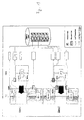
- the figure schematically illustrates a sequence of processing steps PS representing a process plan rather complex in reality.
- the sequence of orders contains a first processing step interrupted upon irregular processing, as well as process steps PS + 1, PS + n - 1 and PS + n.
- To excerpts of the sequence of orders denoted as case I and case II illustrate two preferred embodiments of the invention. They refer to two different ways of integrating unplanned optional mapping steps OMS.
- case I the first part POn of a processing step is interrupted upon irregular processing execution, and a mapping order MO is defined and inserted, thereby creating an order POff for residual execution of the interrupted product processing order to be executed after the mapping order.
- the next process step PS + 1 is executed.
- a dispatch list with orders to be executed is stored, and semiconductor products corresponding to data in the dispatch list are transported to the respective processing tool by a transport system.
- the semiconductor products are transported in groups of one or several lots in containers like front opening unified pots, for instance, with several slots, each slot receiving a single semiconductor wafer. Every processing and mapping order is initiated and concluded by respective movein and move-out sub-orders MVIN and MVOU.
- a mapping order is integrated in the sequence of orders by insertion between two processing orders PS + n - 1 and PS + n.
- mapping orders and, if required, further processing orders, into the order sequence before executing subsequent orders are retrievable.
- a job report JR is created and filed in a database containing history data of every single wafer.
- the history data contain all relevant processing data as well as the position data of the wafer, that is number of the slot of the front opening unified pod and the identification of the unified pod.
- the history data contain all information required for gapless slot and wafer ID related wafer tracking from the beginning to the end of the processing root. According to prior art, the history data did not correspond to the actual wafer positions after diverse handling steps manually performed upon irregular processing, and hence had to be rearranged.
Landscapes
- Container, Conveyance, Adherence, Positioning, Of Wafer (AREA)
- General Factory Administration (AREA)
Priority Applications (8)
| Application Number | Priority Date | Filing Date | Title |
|---|---|---|---|
| EP00117733A EP1180788A1 (en) | 2000-08-17 | 2000-08-17 | Method for wafer position data retrieval in semiconductor wafer manufacturing |
| DE60130896T DE60130896T2 (de) | 2000-08-17 | 2001-08-01 | Verfahren zur wiedergabe von waferpositionsdaten während einer halbleiterwaferherstellung |
| EP01960604A EP1309988B1 (en) | 2000-08-17 | 2001-08-01 | Method for wafer position data retrieval in semiconductor wafer manufacturing |
| PCT/EP2001/008900 WO2002015235A1 (en) | 2000-08-17 | 2001-08-01 | Method for wafer position data retrieval in semiconductor wafer manufacturing |
| JP2002520274A JP2004507082A (ja) | 2000-08-17 | 2001-08-01 | 半導体ウエハ製造においてウエハ位置データを検索する方法 |
| KR10-2003-7001633A KR100523826B1 (ko) | 2000-08-17 | 2001-08-01 | 반도체 웨이퍼 제조시의, 웨이퍼 위치 데이터를 정정하기위한방법 |
| TW090120079A TW503501B (en) | 2000-08-17 | 2001-08-16 | Method for wafer position data retrieval in semiconductor wafer manufacturing |
| US10/368,073 US6909932B2 (en) | 2000-08-17 | 2003-02-18 | Method for wafer position data retrieval in semiconductor wafer manufacturing |
Applications Claiming Priority (1)
| Application Number | Priority Date | Filing Date | Title |
|---|---|---|---|
| EP00117733A EP1180788A1 (en) | 2000-08-17 | 2000-08-17 | Method for wafer position data retrieval in semiconductor wafer manufacturing |
Publications (1)
| Publication Number | Publication Date |
|---|---|
| EP1180788A1 true EP1180788A1 (en) | 2002-02-20 |
Family
ID=8169562
Family Applications (2)
| Application Number | Title | Priority Date | Filing Date |
|---|---|---|---|
| EP00117733A Withdrawn EP1180788A1 (en) | 2000-08-17 | 2000-08-17 | Method for wafer position data retrieval in semiconductor wafer manufacturing |
| EP01960604A Expired - Lifetime EP1309988B1 (en) | 2000-08-17 | 2001-08-01 | Method for wafer position data retrieval in semiconductor wafer manufacturing |
Family Applications After (1)
| Application Number | Title | Priority Date | Filing Date |
|---|---|---|---|
| EP01960604A Expired - Lifetime EP1309988B1 (en) | 2000-08-17 | 2001-08-01 | Method for wafer position data retrieval in semiconductor wafer manufacturing |
Country Status (7)
| Country | Link |
|---|---|
| US (1) | US6909932B2 (https=) |
| EP (2) | EP1180788A1 (https=) |
| JP (1) | JP2004507082A (https=) |
| KR (1) | KR100523826B1 (https=) |
| DE (1) | DE60130896T2 (https=) |
| TW (1) | TW503501B (https=) |
| WO (1) | WO2002015235A1 (https=) |
Families Citing this family (5)
| Publication number | Priority date | Publication date | Assignee | Title |
|---|---|---|---|---|
| US7894174B2 (en) * | 2004-08-23 | 2011-02-22 | Monolithic Power Systems, Inc. | Method and apparatus for fault detection scheme for cold cathode fluorescent lamp (CCFL) integrated circuits |
| CN101453818B (zh) * | 2007-11-29 | 2014-03-19 | 杭州茂力半导体技术有限公司 | 放电灯的电路保护和调节装置 |
| US7826914B2 (en) * | 2008-06-27 | 2010-11-02 | International Business Machines Corporation | System and method for tracking transports in a production process |
| US20110153660A1 (en) * | 2008-10-15 | 2011-06-23 | Inotera Memories, Inc. | Method of searching for key semiconductor operation with randomization for wafer position |
| JP6525500B2 (ja) * | 2014-02-03 | 2019-06-05 | キヤノン株式会社 | パターン形成方法、リソグラフィ装置及び物品の製造方法 |
Citations (2)
| Publication number | Priority date | Publication date | Assignee | Title |
|---|---|---|---|---|
| JPH08268512A (ja) * | 1995-04-03 | 1996-10-15 | Daifuku Co Ltd | 基板仕分け装置を備えた荷保管設備 |
| DE19962703A1 (de) * | 1998-12-23 | 2000-07-06 | Mirae Corp | Verfahren und Vorrichtung zum Steuern des Beladens/Entladens von Halbleiterbauelementen |
Family Cites Families (6)
| Publication number | Priority date | Publication date | Assignee | Title |
|---|---|---|---|---|
| US5761065A (en) * | 1995-03-30 | 1998-06-02 | Advanced Micro Devices, Inc. | Arrangement and method for detecting sequential processing effects in manufacturing |
| US5716856A (en) * | 1995-08-22 | 1998-02-10 | Advanced Micro Devices, Inc. | Arrangement and method for detecting sequential processing effects in manufacturing using predetermined sequences within runs |
| US6259960B1 (en) * | 1996-11-01 | 2001-07-10 | Joel Ltd. | Part-inspecting system |
| TW426872B (en) * | 1999-10-08 | 2001-03-21 | Taiwan Semiconductor Mfg | Method of preventing contamination in process |
| US6684125B2 (en) * | 2000-12-31 | 2004-01-27 | Texas Instruments Incorporated | In-situ randomization and recording of wafer processing order at process tools |
| JP3870052B2 (ja) * | 2001-09-20 | 2007-01-17 | 株式会社日立製作所 | 半導体装置の製造方法及び欠陥検査データ処理方法 |
-
2000
- 2000-08-17 EP EP00117733A patent/EP1180788A1/en not_active Withdrawn
-
2001
- 2001-08-01 JP JP2002520274A patent/JP2004507082A/ja active Pending
- 2001-08-01 WO PCT/EP2001/008900 patent/WO2002015235A1/en not_active Ceased
- 2001-08-01 DE DE60130896T patent/DE60130896T2/de not_active Expired - Lifetime
- 2001-08-01 KR KR10-2003-7001633A patent/KR100523826B1/ko not_active Expired - Fee Related
- 2001-08-01 EP EP01960604A patent/EP1309988B1/en not_active Expired - Lifetime
- 2001-08-16 TW TW090120079A patent/TW503501B/zh not_active IP Right Cessation
-
2003
- 2003-02-18 US US10/368,073 patent/US6909932B2/en not_active Expired - Fee Related
Patent Citations (2)
| Publication number | Priority date | Publication date | Assignee | Title |
|---|---|---|---|---|
| JPH08268512A (ja) * | 1995-04-03 | 1996-10-15 | Daifuku Co Ltd | 基板仕分け装置を備えた荷保管設備 |
| DE19962703A1 (de) * | 1998-12-23 | 2000-07-06 | Mirae Corp | Verfahren und Vorrichtung zum Steuern des Beladens/Entladens von Halbleiterbauelementen |
Non-Patent Citations (2)
| Title |
|---|
| "SORTING AND TRANSFER DRIVE MECHANISM", IBM TECHNICAL DISCLOSURE BULLETIN,US,IBM CORP. NEW YORK, vol. 33, no. 6A, 1 November 1990 (1990-11-01), pages 134 - 143, XP000107661, ISSN: 0018-8689 * |
| PATENT ABSTRACTS OF JAPAN vol. 1997, no. 02 28 February 1997 (1997-02-28) * |
Also Published As
| Publication number | Publication date |
|---|---|
| EP1309988A1 (en) | 2003-05-14 |
| DE60130896T2 (de) | 2008-08-21 |
| TW503501B (en) | 2002-09-21 |
| EP1309988B1 (en) | 2007-10-10 |
| WO2002015235A1 (en) | 2002-02-21 |
| US6909932B2 (en) | 2005-06-21 |
| KR20030064375A (ko) | 2003-07-31 |
| US20030144757A1 (en) | 2003-07-31 |
| JP2004507082A (ja) | 2004-03-04 |
| DE60130896D1 (de) | 2007-11-22 |
| KR100523826B1 (ko) | 2005-10-25 |
Similar Documents
| Publication | Publication Date | Title |
|---|---|---|
| US6778879B2 (en) | Automated material handling system and method of use | |
| US6308107B1 (en) | Realtime decision making system for reduction of time delays in an automated material handling system | |
| US7672748B2 (en) | Automated manufacturing systems and methods | |
| KR102752955B1 (ko) | 에지 링 부품 번호들을 슬롯 번호들에 맵핑하기 위한 식별자 사용 | |
| US20060095153A1 (en) | Wafer carrier transport management method and system thereof | |
| US7151980B2 (en) | Transport management system and method thereof | |
| EP1309988B1 (en) | Method for wafer position data retrieval in semiconductor wafer manufacturing | |
| JP2024547198A (ja) | 半導体プロセスデバイスのスケジューリング制御方法及び半導体プロセスデバイス | |
| CN100337305C (zh) | 测试衬底的回收方法和装置 | |
| US7016753B2 (en) | Management system for production line and management method for production line | |
| US20040237284A1 (en) | Compound processing system for sheet metal processing | |
| US8015040B2 (en) | Methods, systems, and computer program products for product randomization and analysis in a manufacturing environment | |
| US20050096775A1 (en) | Method and system of automatic carrier transfer | |
| US7539553B2 (en) | System and method for automated dispatch and transportation of work-in-process | |
| US6747230B2 (en) | Method and device for sorting wafers | |
| US7302305B2 (en) | Job queue management system and method thereof, including clustering wafer lots processed by common recipe into group, and creating process job and control job | |
| US6338005B1 (en) | Managing test material in an automated material handling system | |
| US7015068B2 (en) | Partial wafer processing for random size wafers | |
| JP2004507082A5 (https=) | ||
| JP4381673B2 (ja) | 生産ラインの管理方法 | |
| CN100428438C (zh) | 在处理工具内交换传送盒的方法和系统 | |
| US7286891B2 (en) | System and method for correcting material and data mismatch in an automated manufacturing environment | |
| TW557480B (en) | Automatic wafer sorting system and method | |
| JPH04273115A (ja) | ロット編成方法および装置 | |
| US20040004167A1 (en) | Paddle for securely mounting a wafer cassette holder thereto |
Legal Events
| Date | Code | Title | Description |
|---|---|---|---|
| PUAI | Public reference made under article 153(3) epc to a published international application that has entered the european phase |
Free format text: ORIGINAL CODE: 0009012 |
|
| AK | Designated contracting states |
Kind code of ref document: A1 Designated state(s): AT BE CH CY DE DK ES FI FR GB GR IE IT LI LU MC NL PT SE |
|
| AX | Request for extension of the european patent |
Free format text: AL;LT;LV;MK;RO;SI |
|
| AKX | Designation fees paid | ||
| REG | Reference to a national code |
Ref country code: DE Ref legal event code: 8566 |
|
| STAA | Information on the status of an ep patent application or granted ep patent |
Free format text: STATUS: THE APPLICATION IS DEEMED TO BE WITHDRAWN |
|
| 18D | Application deemed to be withdrawn |
Effective date: 20020821 |