EP1179839A2 - Process for manufacturing a non-volatile memory cell - Google Patents
Process for manufacturing a non-volatile memory cell Download PDFInfo
- Publication number
- EP1179839A2 EP1179839A2 EP01114948A EP01114948A EP1179839A2 EP 1179839 A2 EP1179839 A2 EP 1179839A2 EP 01114948 A EP01114948 A EP 01114948A EP 01114948 A EP01114948 A EP 01114948A EP 1179839 A2 EP1179839 A2 EP 1179839A2
- Authority
- EP
- European Patent Office
- Prior art keywords
- layer
- polysilicon layer
- gate region
- floating gate
- cell
- Prior art date
- Legal status (The legal status is an assumption and is not a legal conclusion. Google has not performed a legal analysis and makes no representation as to the accuracy of the status listed.)
- Withdrawn
Links
Images


Classifications
-
- H—ELECTRICITY
- H10—SEMICONDUCTOR DEVICES; ELECTRIC SOLID-STATE DEVICES NOT OTHERWISE PROVIDED FOR
- H10B—ELECTRONIC MEMORY DEVICES
- H10B41/00—Electrically erasable-and-programmable ROM [EEPROM] devices comprising floating gates
- H10B41/30—Electrically erasable-and-programmable ROM [EEPROM] devices comprising floating gates characterised by the memory core region
-
- H—ELECTRICITY
- H10—SEMICONDUCTOR DEVICES; ELECTRIC SOLID-STATE DEVICES NOT OTHERWISE PROVIDED FOR
- H10B—ELECTRONIC MEMORY DEVICES
- H10B69/00—Erasable-and-programmable ROM [EPROM] devices not provided for in groups H10B41/00 - H10B63/00, e.g. ultraviolet erasable-and-programmable ROM [UVEPROM] devices
Definitions
- the present invention relates to a process for fabricating a non-volatile memory cell having a floating gate region, which is self-aligned to the insulator, and having a high coefficient of coupling.
- the invention relates, particularly but not exclusively, to a process for fabricating a non-volatile EPROM or flash EPROM cell, and the following description is made with reference to this application field, with the only aim to simplify its explanation.
- electronic memory devices of the type of EPROM's or flash EPROM's, integrated in a semiconductor comprise a plurality of non-volatile memory cells arranged in a matrix array.
- the non-volatile memory cells comprise each a MOS transistor having a gate region, located above the channel region, which is floating, i.e. has a high DC impedance to all the other terminals of the cell and the circuit wherein the cell is incorporated.
- the cell also has a second region, known as the control gate, which is driven by suitable control voltages.
- the other electrodes of the transistor are the standard drain, source, and body terminals.
- Area occupation is defined as the product of the so-called "y-pitch” and “x-pitch” (see Figure 1), i.e. the cell dimensions along respective y and x directions in a plane of lay.
- the "y-pitch" dimension is given by the sum of the cell half-contact dimension, the distance from the contact to the gate region, the length dimension of the gate region, and the half-sourceline.
- the "x-pitch" dimension is given by the width of the memory cell active area, or the dimension of the floating gate region, plus the respective distance.
- Limiting factors to a reduction of the x-pitch dimension are the resolution of the fabricating process and, therefore, in defining the floating gate region, and above all, the alignment tolerances of the floating gate region to the active area.
- this solution has some drawbacks. In fact, it does not solve the problem of providing a good capacitive coupling between the control gate and the floating gate region.
- the coupling could be improved by extending the floating gate region to overlie the layer of field oxide that surrounds the active area of the cell along the x direction.
- several polysilicon layers would have to be aligned to the active area in order to achieve such an improved capacitive coupling, and this structure formation adds problems of alignment and photolithography tolerance to the process steps.
- the technical problem that underlies this invention is to provide a process for fabricating a non-volatile memory cell, whereby a floating gate region can be obtained which is self-aligned to the active area of the cell, and whereby the coupling area between the floating gate region and the control gate region can be maximized. Accordingly, this process should have appropriate structural characteristics to overcome the limitations and drawbacks with which prior art memory cells are still beset.
- the resolutive idea of this invention is to form the floating gate region by a double deposition of polycrystalline silicon (polysilicon), wherein the first deposition allows the floating gate region to be self-aligned to the active area, while the second deposition allows the surface of the floating gate region to be extended as much as possible in the x direction of the cell without presenting lithography alignment problems.
- polysilicon polycrystalline silicon
- the nitride layer 4 could be omitted.
- the polysilicon layer 3 would then be made thicker.
- oxide layer 2 and polycrystalline silicon layer are the definitive ones, that is, those providing the gate oxide layer (or the so-called tunnel oxide, if the cell is a flash type) and the floating gate region of the cell.
- this stack structure was usually formed of sacrificial layers, which were removed after use.
- the thickness dimensions may be, for example: from a few unit to a few ten nm (e.g. 8 to 12 nm) for the oxide layer 2; a few hundred nm (e.g. 100 to 150 nm) for the polysilicon layer 3; and a few hundred nm (e.g. 100 to 200 nm) for the nitride layer 4.
- the layer 5 is patterned to provide a mask approaching in size the active area AA of the cell to be obtained.
- the nitride layer 4, if there, and the polysilicon layer 3 and oxide layer 2 are then etched in cascade.
- This etching is continued to form a trench 6 in the semiconductor layer 1 and define the active area AA of the memory cell.
- the trench 6 will have sloping sidewalls at an angle ⁇ from the surface plane.
- the angle ⁇ may vary between 90 and 60 degrees (and is typically 75-85 degrees).
- the trench 6 is shown as having sloping sidewalls, but it should be understood that the trench 6 may be formed with vertical sidewalls.
- the depth of the trench in the semiconductor substrate 1 is a few hundred nanometers, e.g. about 300 nm.
- the layer 5 of photo-sensitive material is then removed, and an isolation layer 7 is formed to fill the trench 6 and isolate adjacent stack structures from one another.
- This isolation layer 7 is made sufficiently thick to at least partly planarize the structure at this step of its fabrication, as shown in Figure 6.
- the isolation layer 7 may be an oxide layer deposited by a CVD method.
- the process of this invention also comprises the following steps.
- the surface of the structure is further planarized, e.g. by a CMP (Chemical Mechanical Polishing) technique, to expose the nitride layer 4.
- CMP Chemical Mechanical Polishing
- the oxide layer 7 is then etched away for a thickness equal to the combined thicknesses of the nitride layer 4 and the polysilicon layer 3.
- the nitride layer 4 is then etched away by selective chemical etching as shown in Figure 9, and a second layer 8 of polysilicon is deposited as shown in Figure 10.
- the second polysilicon layer 8 is short-circuited to the first polysilicon layer 3.
- the thickness of the second polysilicon layer 8 is equal to that of the first polysilicon layer 3, i.e. is in the range of hundreds of nanometers, e.g. 100 to 150 nm.
- the second polysilicon layer 8 is etched away for a thickness equal to that of the deposited layer 8, e.g. using an etch-back method.
- extensions 9 are formed adjacent to the first polysilicon layer 3, over the isolation layer 7.
- a floating gate region 10 is formed which comprises a first portion located above the active area formed from the first polysilicon area, and has extensions 9 lying over the isolation layer formed from the second polysilicon layer.
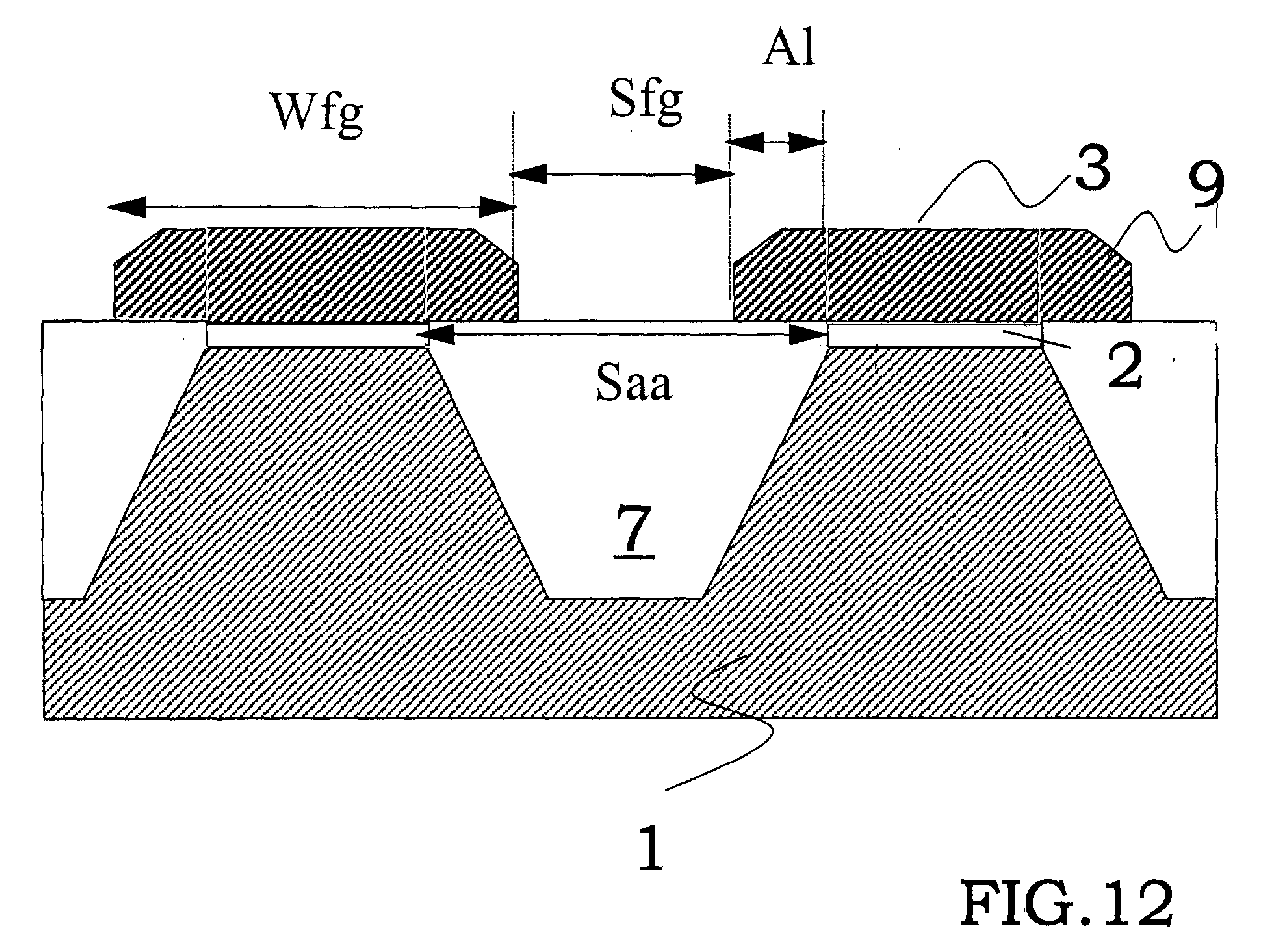
- a cell fabricated in accordance with the invention has a smaller active area width Waa than the distance Saa between contiguous floating gate regions, and has a greater floating gate region width Wfg than the distance Sfg between contiguous floating gate regions.
- This dimensional feature is made necessary by that the dimension of the floating gate region along the direction x contributes to define the capacitive coupling to the control gate, a fundamental parameter to the proper dimensioning of the cell.
- neither dimensions, of the extensions and the floating gate region, are defined by masking, but rather by the thickness of the polysilicon films deposited.
- K the thickness of the polysilicon film deposited (of both the first and second layers)
- the dimensions of the extensions will equal K
- the dimension of the distance between floating gate regions will equal Saa - 2K, where Saa is the distance between active areas.
- the fabricating process set forth hereinabove does solve the technical problem, and offers a number of advantages.
- a major advantage of a memory cell fabricated thereby is that the capacitive coupling of the floating gate region to the control region can be maximized, as shown in Figure 13.
- this can be achieved by maximizing dimension A1 and minimizing dimension Sfg, with a suitably selected thickness K.
Abstract
Description
- depositing a dielectric layer, such as ONO, and then depositing a polysilicon layer to form the control gate region;
- implanting the source and drain regions of the cell; and
- defining the contacts and metal lines.
Claims (7)
- A process for fabricating non-volatile memory cells on a semiconductor substrate comprising the following steps:forming a stack structure comprised of a first polysilicon layer (3) isolated from the substrate by an oxide layer (2);cascade etching the first polysilicon layer (3), oxide layer (2), and semiconductor substrate (1) to define a first portion of a floating gate region of the cell and at least one trench (6) bordering an active area (AA) of the memory cell;filling said at least one trench (6) with an isolation layer (7);depositing a second polysilicon layer (8) onto the whole exposed surface of the semiconductor; andetching away said second polysilicon layer (8) to expose the floating gate region formed in the first polysilicon layer (3), thereby forming extensions (9) adjacent to said portion of the first polysilicon layer (3).
- The process of Claim 1, characterized in that said extensions extend over the isolation layer.
- The process of Claim 1, characterized in that said second polysilicon layer (8) has the same thickness as the first polysilicon layer (3).
- The process of Claim 1, characterized in that the stack structure includes a nitride layer (4).
- The process of Claim 1, characterized in that the trenches (6) have sloping sidewalls from the semiconductor surface.
- The process of Claim 1, characterized in that the trenches (6) have vertical sidewalls from the semiconductor surface.
- The process of Claim 1, characterized in that the isolation layer is an oxide layer.
Applications Claiming Priority (2)
| Application Number | Priority Date | Filing Date | Title |
|---|---|---|---|
| ITMI001567 | 2000-07-11 | ||
| IT2000MI001567A IT1318145B1 (en) | 2000-07-11 | 2000-07-11 | PROCESS FOR MAKING A NON-VOLATILE MEMORY CELL WITH A REGION OF FLOATING GATE SELF-ALIGNED WITH INSULATION AND WITH A HIGH |
Publications (2)
| Publication Number | Publication Date |
|---|---|
| EP1179839A2 true EP1179839A2 (en) | 2002-02-13 |
| EP1179839A3 EP1179839A3 (en) | 2004-12-15 |
Family
ID=11445453
Family Applications (1)
| Application Number | Title | Priority Date | Filing Date |
|---|---|---|---|
| EP01114948A Withdrawn EP1179839A3 (en) | 2000-07-11 | 2001-06-20 | Process for manufacturing a non-volatile memory cell |
Country Status (3)
| Country | Link |
|---|---|
| US (2) | US6537879B2 (en) |
| EP (1) | EP1179839A3 (en) |
| IT (1) | IT1318145B1 (en) |
Cited By (1)
| Publication number | Priority date | Publication date | Assignee | Title |
|---|---|---|---|---|
| KR100426487B1 (en) * | 2001-12-28 | 2004-04-14 | 주식회사 하이닉스반도체 | Method of forming a floating gate in flash memory device |
Families Citing this family (15)
| Publication number | Priority date | Publication date | Assignee | Title |
|---|---|---|---|---|
| US20020130357A1 (en) * | 2001-03-14 | 2002-09-19 | Hurley Kelly T. | Self-aligned floating gate flash cell system and method |
| US6475894B1 (en) * | 2002-01-18 | 2002-11-05 | Nanya Technology Corporation | Process for fabricating a floating gate of a flash memory in a self-aligned manner |
| US6682977B2 (en) * | 2002-02-11 | 2004-01-27 | Winbond Electronics Corporation | Method for fabricating a gate structure of a flash memory |
| KR100436289B1 (en) * | 2002-07-18 | 2004-06-16 | 주식회사 하이닉스반도체 | Gate structure of flash memory cell and method of forming the same and method of forming dielectric layer |
| KR100504691B1 (en) * | 2003-01-10 | 2005-08-03 | 삼성전자주식회사 | Non-volatile memory device having a charge strage insulator and method of fabricating the same |
| KR100511598B1 (en) * | 2003-09-24 | 2005-08-31 | 동부아남반도체 주식회사 | Method of fabricating a flash memory |
| KR100554516B1 (en) * | 2004-06-29 | 2006-03-03 | 삼성전자주식회사 | Method of manufacturing a semiconductor device |
| US20060046402A1 (en) * | 2004-08-31 | 2006-03-02 | Micron Technology, Inc. | Flash cell structures and methods of formation |
| KR100655289B1 (en) * | 2005-01-13 | 2006-12-08 | 삼성전자주식회사 | Method of fabricating flash memory |
| JP2006303308A (en) * | 2005-04-22 | 2006-11-02 | Toshiba Corp | Semiconductor device and its manufacturing method |
| KR100608377B1 (en) * | 2005-05-02 | 2006-08-08 | 주식회사 하이닉스반도체 | Method for fabricating cell transistor of memory device |
| US20070063319A1 (en) * | 2005-09-19 | 2007-03-22 | Bohumil Lojek | Film stack and method for fabricating the same |
| KR100660285B1 (en) * | 2005-12-28 | 2006-12-20 | 동부일렉트로닉스 주식회사 | Method for manufacturing split gate type non-volatile memory device |
| KR100764746B1 (en) | 2006-09-08 | 2007-10-08 | 삼성전자주식회사 | Nonvolatile memory device and method of forming the same |
| CN102299092B (en) | 2010-06-22 | 2013-10-30 | 中国科学院微电子研究所 | Semiconductor device and forming method thereof |
Citations (5)
| Publication number | Priority date | Publication date | Assignee | Title |
|---|---|---|---|---|
| WO1996008840A1 (en) * | 1994-09-13 | 1996-03-21 | Macronix International Co., Ltd. | A flash eprom transistor array and method for manufacturing the same |
| JPH0897306A (en) * | 1994-09-29 | 1996-04-12 | Toshiba Corp | Semiconductor device and its manufacture |
| EP0780902A1 (en) * | 1995-07-31 | 1997-06-25 | Sharp Kabushiki Kaisha | Nonvolatile semiconductor memory and method for fabricating the same |
| WO1999031730A1 (en) * | 1997-12-18 | 1999-06-24 | Advanced Micro Devices, Inc. | Formation of control and floating gates of semiconductor non-volatile memories |
| US6057580A (en) * | 1997-07-08 | 2000-05-02 | Kabushiki Kaisha Toshiba | Semiconductor memory device having shallow trench isolation structure |
Family Cites Families (5)
| Publication number | Priority date | Publication date | Assignee | Title |
|---|---|---|---|---|
| US6140184A (en) * | 1998-06-01 | 2000-10-31 | Motorola, Inc. | Method of changing the power dissipation across an array of transistors |
| TW407381B (en) * | 1999-03-01 | 2000-10-01 | United Microelectronics Corp | Manufacture of the flash memory cell |
| JP2001196476A (en) * | 2000-01-07 | 2001-07-19 | Toshiba Corp | Semiconductor device and its manufacturing method |
| US6326283B1 (en) * | 2000-03-07 | 2001-12-04 | Vlsi Technology, Inc. | Trench-diffusion corner rounding in a shallow-trench (STI) process |
| US6326263B1 (en) * | 2000-08-11 | 2001-12-04 | United Microelectronics Corp. | Method of fabricating a flash memory cell |
-
2000
- 2000-07-11 IT IT2000MI001567A patent/IT1318145B1/en active
-
2001
- 2001-06-20 EP EP01114948A patent/EP1179839A3/en not_active Withdrawn
- 2001-07-06 US US09/900,501 patent/US6537879B2/en not_active Expired - Lifetime
-
2003
- 2003-01-07 US US10/337,556 patent/US6750505B2/en not_active Expired - Lifetime
Patent Citations (5)
| Publication number | Priority date | Publication date | Assignee | Title |
|---|---|---|---|---|
| WO1996008840A1 (en) * | 1994-09-13 | 1996-03-21 | Macronix International Co., Ltd. | A flash eprom transistor array and method for manufacturing the same |
| JPH0897306A (en) * | 1994-09-29 | 1996-04-12 | Toshiba Corp | Semiconductor device and its manufacture |
| EP0780902A1 (en) * | 1995-07-31 | 1997-06-25 | Sharp Kabushiki Kaisha | Nonvolatile semiconductor memory and method for fabricating the same |
| US6057580A (en) * | 1997-07-08 | 2000-05-02 | Kabushiki Kaisha Toshiba | Semiconductor memory device having shallow trench isolation structure |
| WO1999031730A1 (en) * | 1997-12-18 | 1999-06-24 | Advanced Micro Devices, Inc. | Formation of control and floating gates of semiconductor non-volatile memories |
Non-Patent Citations (1)
| Title |
|---|
| PATENT ABSTRACTS OF JAPAN vol. 1996, no. 08, 30 August 1996 (1996-08-30) -& JP 08 097306 A (TOSHIBA CORP), 12 April 1996 (1996-04-12) * |
Cited By (1)
| Publication number | Priority date | Publication date | Assignee | Title |
|---|---|---|---|---|
| KR100426487B1 (en) * | 2001-12-28 | 2004-04-14 | 주식회사 하이닉스반도체 | Method of forming a floating gate in flash memory device |
Also Published As
| Publication number | Publication date |
|---|---|
| IT1318145B1 (en) | 2003-07-23 |
| EP1179839A3 (en) | 2004-12-15 |
| ITMI20001567A1 (en) | 2002-01-11 |
| US20030096477A1 (en) | 2003-05-22 |
| ITMI20001567A0 (en) | 2000-07-11 |
| US6537879B2 (en) | 2003-03-25 |
| US20020025631A1 (en) | 2002-02-28 |
| US6750505B2 (en) | 2004-06-15 |
Similar Documents
| Publication | Publication Date | Title |
|---|---|---|
| US6885058B2 (en) | Semiconductor device and method of manufacturing such a semiconductor device | |
| US7745875B2 (en) | Method for producing a vertical field effect transistor | |
| US6391722B1 (en) | Method of making nonvolatile memory having high capacitive coupling ratio | |
| US7208796B2 (en) | Split gate flash memory | |
| US6537879B2 (en) | Process for manufacturing a non-volatile memory cell with a floating gate region autoaligned to the isolation and with a high coupling coefficient | |
| US6235589B1 (en) | Method of making non-volatile memory with polysilicon spacers | |
| US20020190305A1 (en) | Nonvolatile memories with floating gate spacers, and methods of fabrication | |
| US7951670B2 (en) | Flash memory cell with split gate structure and method for forming the same | |
| US20070111442A1 (en) | Method of making a multi-bit nanocrystal memory | |
| US6451652B1 (en) | Method for forming an EEPROM cell together with transistor for peripheral circuits | |
| US6717224B2 (en) | Flash memory cell and method for fabricating a flash | |
| US20150243670A1 (en) | Nonvolatile semiconductor memory device having element isolating region of trench type | |
| KR20040023716A (en) | Method of manufacturing a semiconductor device with a non-volatile memory comprising a memory cell with an access gate and with a control gate and a charge storage region | |
| US6787843B2 (en) | Nonvolatile semiconductor memory cell and associated semiconductor circuit configuration and method for the fabrication of the circuit configuration | |
| US6472259B1 (en) | Method of manufacturing semiconductor device | |
| US11640972B2 (en) | Process for fabricating a high-voltage capacitive element, and corresponding integrated circuit | |
| JP3764177B2 (en) | Semiconductor memory device and manufacturing method thereof | |
| EP1032029A1 (en) | Process for manufacturing semiconductor integrated electronic memory devices having a virtual ground cells matrix | |
| US20240030302A1 (en) | Memory device | |
| US20020063275A1 (en) | Method of forming transistor gate | |
| US7550342B2 (en) | Nonvolatile semiconductor memory device and method of manufacturing the same |
Legal Events
| Date | Code | Title | Description |
|---|---|---|---|
| PUAI | Public reference made under article 153(3) epc to a published international application that has entered the european phase |
Free format text: ORIGINAL CODE: 0009012 |
|
| AK | Designated contracting states |
Kind code of ref document: A2 Designated state(s): AT BE CH CY DE DK ES FI FR GB GR IE IT LI LU MC NL PT SE TR |
|
| AX | Request for extension of the european patent |
Free format text: AL;LT;LV;MK;RO;SI |
|
| RIN1 | Information on inventor provided before grant (corrected) |
Inventor name: RATTI STEFANO Inventor name: CAMERLENGHI, EMILIO Inventor name: BEZ, ROBERTO |
|
| RIN1 | Information on inventor provided before grant (corrected) |
Inventor name: RATTI STEFANO Inventor name: CAMERLENGHI, EMILIO Inventor name: BEZ, ROBERTO |
|
| PUAL | Search report despatched |
Free format text: ORIGINAL CODE: 0009013 |
|
| AK | Designated contracting states |
Kind code of ref document: A3 Designated state(s): AT BE CH CY DE DK ES FI FR GB GR IE IT LI LU MC NL PT SE TR |
|
| AX | Request for extension of the european patent |
Extension state: AL LT LV MK RO SI |
|
| RIC1 | Information provided on ipc code assigned before grant |
Ipc: 7H 01L 21/28 B Ipc: 7H 01L 21/8247 B Ipc: 7H 01L 21/336 A |
|
| 17P | Request for examination filed |
Effective date: 20050609 |
|
| AKX | Designation fees paid |
Designated state(s): DE FR GB IT |
|
| STAA | Information on the status of an ep patent application or granted ep patent |
Free format text: STATUS: THE APPLICATION IS DEEMED TO BE WITHDRAWN |
|
| 18D | Application deemed to be withdrawn |
Effective date: 20060514 |