EP0780902A1 - Nonvolatile semiconductor memory and method for fabricating the same - Google Patents
Nonvolatile semiconductor memory and method for fabricating the same Download PDFInfo
- Publication number
- EP0780902A1 EP0780902A1 EP96305665A EP96305665A EP0780902A1 EP 0780902 A1 EP0780902 A1 EP 0780902A1 EP 96305665 A EP96305665 A EP 96305665A EP 96305665 A EP96305665 A EP 96305665A EP 0780902 A1 EP0780902 A1 EP 0780902A1
- Authority
- EP
- European Patent Office
- Prior art keywords
- polysilicon
- films
- semiconductor substrate
- oxide film
- tunnel oxide
- Prior art date
- Legal status (The legal status is an assumption and is not a legal conclusion. Google has not performed a legal analysis and makes no representation as to the accuracy of the status listed.)
- Granted
Links
- 239000004065 semiconductor Substances 0.000 title claims abstract description 104
- 238000000034 method Methods 0.000 title claims description 36
- 229910021420 polycrystalline silicon Inorganic materials 0.000 claims abstract description 166
- 229920005591 polysilicon Polymers 0.000 claims abstract description 166
- 239000000758 substrate Substances 0.000 claims abstract description 88
- 239000011159 matrix material Substances 0.000 claims abstract description 11
- 238000009792 diffusion process Methods 0.000 claims description 50
- 239000012535 impurity Substances 0.000 claims description 35
- 230000008878 coupling Effects 0.000 claims description 23
- 238000010168 coupling process Methods 0.000 claims description 23
- 238000005859 coupling reaction Methods 0.000 claims description 23
- 238000000151 deposition Methods 0.000 claims description 12
- 239000011810 insulating material Substances 0.000 claims description 11
- 238000000206 photolithography Methods 0.000 claims description 10
- 238000002955 isolation Methods 0.000 claims description 8
- 238000000059 patterning Methods 0.000 claims description 8
- 230000015572 biosynthetic process Effects 0.000 claims description 6
- 238000005530 etching Methods 0.000 claims description 4
- 238000004519 manufacturing process Methods 0.000 description 12
- VYPSYNLAJGMNEJ-UHFFFAOYSA-N Silicium dioxide Chemical compound O=[Si]=O VYPSYNLAJGMNEJ-UHFFFAOYSA-N 0.000 description 11
- 230000001133 acceleration Effects 0.000 description 7
- 229920002120 photoresistant polymer Polymers 0.000 description 7
- -1 boron ions Chemical class 0.000 description 5
- 238000005229 chemical vapour deposition Methods 0.000 description 5
- 230000003647 oxidation Effects 0.000 description 5
- 238000007254 oxidation reaction Methods 0.000 description 5
- 229910052581 Si3N4 Inorganic materials 0.000 description 4
- 229910052681 coesite Inorganic materials 0.000 description 4
- 229910052906 cristobalite Inorganic materials 0.000 description 4
- 239000000377 silicon dioxide Substances 0.000 description 4
- HQVNEWCFYHHQES-UHFFFAOYSA-N silicon nitride Chemical compound N12[Si]34N5[Si]62N3[Si]51N64 HQVNEWCFYHHQES-UHFFFAOYSA-N 0.000 description 4
- 229910052682 stishovite Inorganic materials 0.000 description 4
- 229910052905 tridymite Inorganic materials 0.000 description 4
- 229910052785 arsenic Inorganic materials 0.000 description 3
- 229910052796 boron Inorganic materials 0.000 description 3
- 238000010586 diagram Methods 0.000 description 3
- 150000002500 ions Chemical class 0.000 description 3
- 239000000463 material Substances 0.000 description 3
- 229910052814 silicon oxide Inorganic materials 0.000 description 3
- 230000008018 melting Effects 0.000 description 2
- 238000002844 melting Methods 0.000 description 2
- 229910052751 metal Inorganic materials 0.000 description 2
- 239000002184 metal Substances 0.000 description 2
- 150000004767 nitrides Chemical class 0.000 description 2
- 239000012299 nitrogen atmosphere Substances 0.000 description 2
- 229910021332 silicide Inorganic materials 0.000 description 2
- FVBUAEGBCNSCDD-UHFFFAOYSA-N silicide(4-) Chemical compound [Si-4] FVBUAEGBCNSCDD-UHFFFAOYSA-N 0.000 description 2
- WNUPENMBHHEARK-UHFFFAOYSA-N silicon tungsten Chemical compound [Si].[W] WNUPENMBHHEARK-UHFFFAOYSA-N 0.000 description 2
- CIWBSHSKHKDKBQ-JLAZNSOCSA-N Ascorbic acid Chemical compound OC[C@H](O)[C@H]1OC(=O)C(O)=C1O CIWBSHSKHKDKBQ-JLAZNSOCSA-N 0.000 description 1
- OAICVXFJPJFONN-UHFFFAOYSA-N Phosphorus Chemical compound [P] OAICVXFJPJFONN-UHFFFAOYSA-N 0.000 description 1
- XUIMIQQOPSSXEZ-UHFFFAOYSA-N Silicon Chemical compound [Si] XUIMIQQOPSSXEZ-UHFFFAOYSA-N 0.000 description 1
- 238000003491 array Methods 0.000 description 1
- RQNWIZPPADIBDY-UHFFFAOYSA-N arsenic atom Chemical compound [As] RQNWIZPPADIBDY-UHFFFAOYSA-N 0.000 description 1
- 230000001419 dependent effect Effects 0.000 description 1
- 230000002542 deteriorative effect Effects 0.000 description 1
- 230000005684 electric field Effects 0.000 description 1
- 239000002784 hot electron Substances 0.000 description 1
- 230000002401 inhibitory effect Effects 0.000 description 1
- 230000010354 integration Effects 0.000 description 1
- 238000012986 modification Methods 0.000 description 1
- 230000004048 modification Effects 0.000 description 1
- 229910052698 phosphorus Inorganic materials 0.000 description 1
- 239000011574 phosphorus Substances 0.000 description 1
- 238000005498 polishing Methods 0.000 description 1
- 229910052710 silicon Inorganic materials 0.000 description 1
- 239000010703 silicon Substances 0.000 description 1
- 238000009751 slip forming Methods 0.000 description 1
- 239000000126 substance Substances 0.000 description 1
- WQJQOUPTWCFRMM-UHFFFAOYSA-N tungsten disilicide Chemical compound [Si]#[W]#[Si] WQJQOUPTWCFRMM-UHFFFAOYSA-N 0.000 description 1
- 229910021342 tungsten silicide Inorganic materials 0.000 description 1
Images


Classifications
-
- H—ELECTRICITY
- H10—SEMICONDUCTOR DEVICES; ELECTRIC SOLID-STATE DEVICES NOT OTHERWISE PROVIDED FOR
- H10B—ELECTRONIC MEMORY DEVICES
- H10B41/00—Electrically erasable-and-programmable ROM [EEPROM] devices comprising floating gates
- H10B41/30—Electrically erasable-and-programmable ROM [EEPROM] devices comprising floating gates characterised by the memory core region
-
- H—ELECTRICITY
- H10—SEMICONDUCTOR DEVICES; ELECTRIC SOLID-STATE DEVICES NOT OTHERWISE PROVIDED FOR
- H10B—ELECTRONIC MEMORY DEVICES
- H10B69/00—Erasable-and-programmable ROM [EPROM] devices not provided for in groups H10B41/00 - H10B63/00, e.g. ultraviolet erasable-and-programmable ROM [UVEPROM] devices
-
- H—ELECTRICITY
- H10—SEMICONDUCTOR DEVICES; ELECTRIC SOLID-STATE DEVICES NOT OTHERWISE PROVIDED FOR
- H10D—INORGANIC ELECTRIC SEMICONDUCTOR DEVICES
- H10D30/00—Field-effect transistors [FET]
- H10D30/60—Insulated-gate field-effect transistors [IGFET]
- H10D30/68—Floating-gate IGFETs
- H10D30/6891—Floating-gate IGFETs characterised by the shapes, relative sizes or dispositions of the floating gate electrode
Definitions
- the present invention relates to a nonvolatile semiconductor memory having floating gates and a method for fabricating such a nonvolatile semiconductor memory.
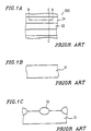
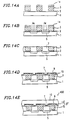
- Figure 1A is a plan view illustrating a first step of the fabrication process of a conventional flash memory
- Figures 1B and 1C are sectional views taken along lines B-B and C-C of Figure 1A, respectively.
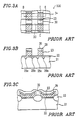
- Figure 2A is a plan view illustrating a second step of the fabrication process of the flash memory
- Figures 2B and 2C are sectional views taken along lines B-B and C-C of Figure 2A, respectively.
- Figure 3A is a plan view illustrating a third step of the fabrication process of the flash memory, and Figures 3B and 3C are sectional views taken along lines B-B and C-C of Figure 3A, respectively.
- LOCOS oxide films 33 are formed on a semiconductor substrate 21 of a memory cell array 500 The portions of the semiconductor substrate 21 which are not covered with the LOCOS oxide films 33 will remain active regions 34.
- tunnel oxide films 22 are formed on the active regions 34 of the semiconductor substrate 21, and polysilicon films which are to be floating gates 23 are formed on the tunnel oxide films 22 so as to cover the entire active regions 34.
- the LOCOS oxide films 33 are ten times or more thicker than the tunnel oxide films 22 and are used as isolators.
- the floating gates 23 are formed so as to overlap the periphery portions of the LOCOS oxide films 33.
- the top surface area of each floating gate 23 is larger than the area thereof in contact with the tunnel oxide film 22.
- ONO (SiO 2 /SiN/SiO 2 ) films 29 are formed to cover the floating gates 23 and a material for the control gates is deposited on the resultant substrate.
- a resist having a pattern of the control gates (word lines) is formed on the deposited material.
- the material for the control gates and the ONO films 29 are etched to form control gates 30 as well as the floating gates 23.
- ions are implanted in the semiconductor substrate 21 using the control gates 30 as a mask, to form source diffusion layers 25a and drain diffusion layers 25b.
- V CG V CG ⁇ C 2 /(C 1 +C 2 ).
- the floating gates 23 extend so as to overlap the LOGOS films 33 in order to increase the coupling ratio. This causes a problem of increasing the cell area.
- Impurity diffusion layers may be used as isolators in place of the thick insulating films.
- the coupling capacitance C 2 between the floating gate and the control gate cannot be made larger than the coupling capacitance C 1 between the floating gate and the semiconductor substrate by overlapping the floating gate with the impurity diffusion layers. It is therefore difficult to increase the coupling ratio in this case, unlike the case where the thick insulating films are used as isolators.
- the nonvolatile semiconductor memory of this invention includes a memory cell array having memory cells arranged in a matrix, the memory cell array comprising: a semiconductor substrate; a tunnel oxide film formed on the semiconductor substrate; floating gates including first polysilicon films formed on the tunnel oxide film and second polysilicon films formed on both sides of the respective first polysilicon films; first insulating films formed on the floating gates; and control gates formed on the first insulating films, wherein the memory cell array further comprising second insulating films formed on the tunnel oxide film between the first polysilicon films, the second insulating films having a predetermined thickness which is thinner than that of the first polysiiicon films, and wherein the second polysilicon films are formed on the second insulating films.
- the nonvolatile semiconductor memory includes a memory cell array having memory cells arranged in a matrix, the memory cell array comprising: a semiconductor substrate; a tunnel oxide film formed on the semiconductor substrate; floating gates including a first polysilicon film formed on the tunnel oxide film and a third polysilicon film formed on the first polysilicon film; first insulating films formed on the floating gates; and control gates formed on the first insulating films, wherein the memory cell array further comprising second insulating films formed on the tunnel oxide film between the first polysilicon films, the second insulating films having a thickness which is substantially same as that of the first polysilicon films, whereby a surface including surfaces of the first polysilicon films and surfaces of the second insulating films being planarized, and wherein each of the third polysilicon film covering the corresponding first polysilicon film and portions of the second insulating films, a surface area of the third polysilicon film being larger than that of the first polysilicon film.
- the second insulating films prevent capacitive coupling between the corresponding second polysilicon films of the floating gates and the semiconductor substrate.
- the method of the present inventon is a method for fabricating a nonvolatile semiconductor memory including a memory cell array having memory cells arranged in a matrix, the memory cell array including a tunnel oxide film, floating gates, first insulating films, and control gates formed in this order on a semiconductor substrate.
- the method comprising the steps of: forming the tunnel oxide film on the semiconductor substrate; depositing first polysilicon on the tunnel oxide film and patterning the first polysilicon into a desired shape by photolithography to form first polysilicon films; depositing second insulating material on the entire surface of the resultant substrate and etching back the deposited second insulating material to form second insulating films on the tunnel oxide film between the first polysilicon films, the second insulating films having a predetermined thickness which is thinner than that of the first polysilicon films; and depositing second polysilicon on the entire surface of the resultant substrate and etching back the second polysilicon to form second polysilicon films on both Sides of the first polysilicon films, wherein each of the first polysilicon films and the corresponding second polysilicon films constitute the floating gates.
- the method of the present invention is a method for fabricating a nonvolatile semiconductor memory including a memory cell array having memory cells arranged in a matrix, the memory cell array including a tunnel oxide film, floating gates, first insulating films, and control gates formed in this order on a semiconductor substrate.
- the method comprising the steps of: forming the tunnel oxide film on the semiconductor substrate; depositing first polysilicon on the tunnel oxide film and patterning the first polysilicon into a desired shape by photolithography to form first polysilicon films; depositing second insulating material on the entire surface of the resultant substrate and removing the second insulating material until the first polysilicon films are exposed, to form second insulating films, and planarizing a surface including surfaces of the first polysilicon films and surfaces of the second insulating films; and depositing third polysilicon on the entire surface of the resultant substrate and patterning the third polysilicon to form third polysilicon films, each of the third polysilicon films covering the corresponding first polysilicon film, a surface area of each third polysilicon film being larger than that of the corresponding first polysilicon films, wherein the first polysilicon films and the corresponding third polysilicon films constitute the respective floating gates.
- the method further comprises a step of forming impurity diffusion regions as isolators by implanting impurities of a same conductivity type as that of the semiconductor substrate in the semiconductor substrate using the control gates as a mask.
- each floating gate includes the first polysilicon film and either the second polysilicon films or the third polysilicon film.
- An insulating film with a predetermined thickness is formed between the semiconductor substrate and the second or third polysilicon film.
- the second polysilicon films are formed in the narrow spaces between sections of the first polysilicon films having a minimum width in the channel length direction. Therefore, the formation of the second polysilicon films does not increase the cell area.
- the invention described herein makes possible the advantages of (1) providing a nonvolatile semiconductor memory where the coupling ratio can be increased without increasing the cell area even when impurity diffusion regions are used as isolators in place of thick insulating isolators, and (2) providing a method for fabricating such a nonvolatile semiconductor memory.
- Figure 1A is a plan view illustrating a first step of the fabrication process of a conventional flash memory.
- Figures 1B and 1C are sectional views taken along lines B-B and C-C of figure 1A, respectively.
- Figure 2A is a plan view illustrating a second step of the fabrication process of the conventional flash memory
- Figures 2B and 2C are sectional views taken along lines B-B and C-C of Figure 2A, respectively.
- Figure 3A is a plan view illustrating a third step of the fabrication process of the conventional flash memory.
- Figures 3B and 3C are sectional views taken along lines B-B and C-C of Figure 3A, respectively.
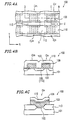
- Figure 4A is a plan view illustrating a flash memory of a virtual ground architecture.
- Figures 4B and 4C are sectional views taken along lines B-B and C-C of Figure 4A, respectively.
- Figure 5A is a plan view illustrating a nonvolatile semiconductor memory of Example 1 according to the present invention.
- Figures 5B and 5C are sectional views taken along lines B-B and C-C of Figure 5A, respectively.
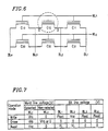
- Figure 6 is an equivalent circuit diagram of the nonvolatile semiconductor memory of the virtual ground architecture.
- Figure 7 is a table showing the conditions in the write, erase, and read operations in Example 1.
- Figures 8A to 8G are sectional views illustrating the steps of the fabrication process of the nonvolatile semiconductor memory of Example 1.
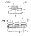
- Figure 9 is a sectional view of a nonvolatile semiconductor memory using LOCOS films as isolators according to the present invention.
- Figure 10 is a sectional view of a nonvolatile semiconductor memory of Example 2 according to the present invention.
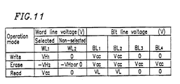
- Figure 11 is a table showing the conditions in the write, erase, and read operations in Example 2.
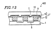
- Figure 13 is a sectional view of a nonvolatile semiconductor memory of Example 3 according to the present invention.
- Figure 4A is a plan view of a memory cell array 100 of a flash memory of the virtual ground architecture.
- Figures 4B and 4C are sectional views taken along lines B-B and C-C of Figure 4A, respectively.
- a control gate 110 is formed on the floating gate 103 via an insulating film 109 made of ONO (SiO 2 /SiN/SiO 2 ) and the like. Such control gates 110 extend in a channel direction of the memory cell C (an X direction shown in Figure 4A), constituting a word line for connecting the memory cells C lined in the X direction.
- an impurity diffusion layer 105 is formed between every two memory cells adjacent each other in the X direction (e.g., memory cells C in and C in ).
- the impurity diffusion layer 105 serves as a drain diffusion layer for one of the two adjacent memory cells (e.g., the memory cell C in ) and a source diffusion layer for the other memory cell (e.g., the memory cell C in ).
- the impurity diffusion layer 105 is thus shared by the two adjacent memory cells.
- the impurity diffusion layers 105 lined in the Y direction are connected with one another via diffusion layer wirings, forming a so-called buried bit line 112, as shown in Figure 4A.
- the bit line 112 serves as a source line or a drain line depending on the memory cell selected.
- the impurity diffusion layer 105 is shared by two memory cells adjacent in the X direction, the impurity diffusion layer 105 acting as the source diffusion layer for one memory cell and the drain diffusion layer for the other memory cell. This eliminates the necessity of isolating the source diffusion layer and the drain diffusion layer of memory cells adjacent in the X direction.
- the bit line 112 can be formed by connecting the impurity diffusion layers 105 for the memory cells lined in the Y direction. This eliminates the necessity of forming a contact region for connecting the bit line with each memory cell, allowing the memory cell array 100 to achieve a high degree of integration.
- memory cell arrays other than the virtual ground architecture can also be used as long as there is formed an insulating film of a predetermined thickness which blocks the generation of a capacitance between a second polysilicon film and a floating gate according to the present invention and the semiconductor substrate.
- Figure 5A is a plan view of a memory cell array 200 of the nonvolatile semiconductor memory of Example 1 according to the present invention.
- Figures 5a and 5C are sectional views taken along lines B-B and C-C of Figure 5A, respectively.
- the same components are denoted by the same reference numerals as those in Figures 4A to 4C.
- the memory cell array 200 of this example includes a p-type semiconductor substrate 1, a tunnel insulating film 2 formed on the semiconductor substrate 1, first polysilicon films 3 formed on the semiconductor substrate 1 formed on the tunnel insulating film 2, and second polysilicon films 8.
- the first and second polysilicon films 3 and 8 constitute floating gates 3'.
- An ONO film 9 covers each of the floating gates 3' composed of the first and second polysilicon films 3 and 8, and a control gate 10 is formed over the ONO film 9. As shown in Figure 5A, the control gates 10 are formed on all memory cells lined in the X direction and are electrically connected, forming a word line.
- a high-density impurity diffusion layer (N - ) 5 and a low-density impurity diffusion layer (N - ) 6 are formed between every two memory cells adjacent in the X direction, and these diffusion layers for the memory cells aligned in the Y direction are connected to form a bit line 12.
- the first polysilicon film 3 of each memory cell capacitively couples with the high-density impurity diffusion layer 5 on the drain side via the tunnel insulating film 2, while the first polysilicon film 3 capacitively couples with the low-density impurity diffusion layer 6 on the source side via the tunnel insulating film 2, forming an asymmetric source/drain structure.
- the tunnel insulating film 2 may be a silicon oxide film or a double-layer structure of a silicon oxide film and a silicon nitride film.
- bit lines BL (bit lines BL 1 to BL 4 are shown in Figure 6) serve as source wirings or drain wirings depending on the selected cell.
- Figure 7 shows the operation conditions when the memory cell C 12 shown in Figure 6 is selected, for example.
- the source voltage V cc is also applied to the control gate 10 of the memory cell, for example, a memory cell C 11 , which is not selected (hereinafter such a memory cell is referred to as a "non-selected cell") and which is connected to the bit line BL 2 on the source side.
- the low-density impurity diffusion layer 6 which does not generate the tunnel phenomenon between the source (low-density impurity diffusion layer 6) and the floating gate is formed on the source side of the non-selected cell C 11 , no tunnel current flows between the Source and the floating gate 3' of the non-selected cell C 11 , thereby inhibiting data from being written in the non-selected cell C 11 .
- a predetermined voltage V cc (4 V, for example) is applied to the word line WL 1
- a predetermined voltage V L (1 V, for example) is applied to the bit line BL 2 and 0 V to the bit line BL 3 , as in the conventional manner, so as to detect a current flowing between the bit lines BL 2 and BL 3 .
- the voltages shown in the table of Figure 7 have the relationship of VH 1 , VH 2 > V cc > V L .
- the tunnel oxide film 2 with a thickness of about 8 nm is formed on the semiconductor substrate 1 by thermal oxidation.
- first polysilicon is deposited on the entire surface of the resultant substrate to a thickness of about 100 to 200 nm.
- the resultant first polysilicon layer is patterned by photolithography using a photoresist 4 to form the first polysilicon films 3 which are to constitute the floating gates in the shape of stripes extending in the channel width direction ( Figure 8A).
- arsenic (As) ions are obliquely implanted in the semiconductor substrate 1 at an angle of 7° from the normal of the semiconductor substrate 1 under the conditions of an acceleration energy of 70 KeV and a dose amount of 1 ⁇ 10 15 /cm 2 using the pattern of the photoresist 4 and the first polysilicon films 3 as a mask, so as to form the high-density impurity diffusion layers 5 which are to be the bit lines ( Figure 8B).
- phosphorus (P) ions are implanted in the semiconductor substrate 1 under the conditions of an acceleration energy of 50 KeV and a dose amount of 3 ⁇ 10 13 /cm 2 using the pattern of the first polysilicon films 3 as a mask, so as. to form the low-density impurity diffusion layers 6 ( Figure 8C).
- the resultant substrate is heat-treated in a nitrogen atmosphere at 900°C for 10 minutes, so that the drain diffusion layers of a DDD structure and the source diffusion layers of an LDD structure are formed ( Figure SD).
- insulating material is then deposited by chemical vapor deposition (CVD) to cover the first polysilicon films 3 and etched back, so that insulating films 7 with a thickness 5 to 10 times larger than that of the tunnel insulating film 2 are formed between the first polysilicon films 3.
- the insulating films 7 serve to prevent a coupling capacitance from generating between the second polysilicon films 8 (part of the floating gates) to be formed in a later stage and the semiconductor substrate 1. That is, portions where the relatively thick insulating films 7 are formed do not contribute the capacitive coupling of the floating gates 3' and the semiconductor substrate 1 ( Figure 8E).
- a second polysilicon is deposited on the entire surface of the resultant substrate and etched back, so as to form second polysilicon films 8 on the sides of the first polysilicon films 3 in such a manner that they are electrically connected with each other. Thereafter, the ONO film 9 is formed on the resultant substrate ( Figure 8F).
- a fourth polysilicon film is formed on the ONO film 9.
- the control gates 10, the insulating films 9, and the floating gates 3' are formed ( Figure 8G).
- the control gates 10 of respective memory cells are formed consecutively in the X direction, forming one word line.
- control gates 10 i.e., the word line WL
- the control gates 10 may be of a double-layered structure including the fourth polysilicon film and a metal silicide film with a high melting point such as tungsten silicide (WSi).
- boron ions are implanted in the semiconductor substrate 1 under the conditions of an acceleration energy of 40 KeV and a dose amount of 1 ⁇ 10 13 /cm 2 using the word lines as a mask, so as to form p-type impurity diffusion layers 11 as isolators (see Figure 5C).
- the isolation is performed by junction isolation.
- the present invention is also applicable to the case where the isolation is performed by forming thick insulating films such as LOCOS films.
- LOCOS films 13 are formed on the semiconductor substrate 1 before the formation of the tunnel insulating film 2 and the first polysilicon films 3.
- the floating gates 3' composed of the first polysilicon films 3 and the second polysilicon films 8 are continuously formed in a shape of stripes. Alternatively, they may be formed separately from one another, and the fourth polysilicon film may be patterned so that the resultant word lines completely cover the floating gates.
- the overlap of the floating gate with the LOCOS film 13 can be minimized because the overlap is required only for an aligning allowance at photolithography.
- Figure 10 is a sectional view of a memory cell array 300 of the nonvolatile semiconductor memory of Example 2 according to the present invention.
- the same components are denoted by the same reference numerals as those in Figures 5A to 5C.
- the memory cell array 300 of this example is the same as the memory cell array 200 of Example 1, except that the low-density impurity diffusion layers 6 are not formed in this example.
- Figure 11 shows the conditions of each operation mode when the nonvolatile semiconductor memory of this example is used. The conditions are shown with reference to the circuit diagram of Figure 6, as in Example 1.
- a high voltage VH 1 (8 V, for example) is applied to the word line WL 1 connected to the selected cell C 12 .
- a predetermined power voltage V cc (4 V, for example) is applied to the bit line BL 2 , one of the two bit lines connected to the selected cell C 12 , while 0 V is applied to the other bit line BL 3 .
- V cc 4 V, for example
- the non-selected cells voltages are applied to two bit lines which are connected to each non-selected cell so that the two bit lines have the same voltage.
- a negative voltage -VH 2 (-12 V, for example) is applied to the word line WL 1
- a predetermined positive voltage V cc (4 V, for example) is applied to all or part of the bit lines, allowing a Fowler-Nordheim (FN) tunnel current to flow.
- V cc 4 V, for example
- the tunnel oxide film 2 with a thickness of about 8 nm is formed on the semiconductor substrate 1 by thermal oxidation.
- first polysilicon is deposited on the entire surface of the resultant substrate to a thickness of about 100 to 200 nm.
- the resultant first polysilicon layer is patterned by photolithography using a photoresist 4 to form the first polysilicon films 3 which are to constitute the floating gates in the shape of stripes extending in the channel width direction.
- arsenic ions are implanted in the semiconductor substrate 1 under the conditions of an acceleration energy of 70 KeV and a dose amount of 1 ⁇ 10 15 /cm 2 using the pattern of the photoresist 4 and the first polysilicon films 3 as a mask, so as to form the high-density impurity diffusion layers 5 which are to be the bit lines ( Figure 12A).
- the resultant substrate is heat-treated in a nitrogen atmosphere at 900°C for 10 minutes, so as to form the diffusion layers ( Figure 12B).
- An insulating material is then deposited by CVD to cover the first polysilicon films 3 and etched back, so that insulating films 7 with a thickness 5 to 10 times larger than that of the tunnel insulating film 2 are formed between the first polysilicon films 3 ( Figure 12C).
- second polysilicon is deposited on the entire surface of the resultant substrate and etched back, so as to form second polysilicon films 8 on the sides of the first polysilicon films 3 in such a manner that they are electrically connected with each other. Thereafter, the ONO film 9 is formed on the resultant substrate ( Figure 12D).
- a fourth polysilicon film is formed on the ONO film 9.
- the control gates 10, the insulating films 9, and the floating gates 3' are formed ( Figure 12E).
- the control gates 10 of respective memory cells are formed consecutively in the X direction, forming one word line.
- control gates 10 i.e., the word line WL
- the control gates 10 may be of a double-layered structure including the fourth polysilicon film and a metal silicide film with a high melting point such as tungsten silicide (WSi).
- boron ions are implanted in the semiconductor substrate 1 under the conditions of an acceleration energy of 40 KeV and a dose amount of 1 ⁇ 10 13 /cm 2 using the word lines as a mask, so as to form p-type impurity diffusion layers 11 as isolators.
- LOCOS films also may be used as isolators.
- Figure 13 is a sectional view of a memory cell array 400 of the nonvolatile semiconductor memory of Example 3 according to the present invention.
- the same components are denoted by the same reference numerals as those in Figures 5A to 5C.
- the tunnel oxide film 2 with a thickness of about 8 nm is formed on the semiconductor substrate 1 by thermal oxidation.
- first polysilicon is deposited on the entire surface of the resultant substrate to a thickness of about 100 to 200 nm, and then silicon nitride is deposited on the first polysilicon layer to a thickness of 10 to 20 nm.
- the resultant first polysilicon layer and the nitride layer are patterned by photolithography using a photoresist to form first polysilicon films 3 which are to constitute the floating gates covering the channel regions and nitride films 14 in a shape of stripes extending in the channel width direction ( Figure 14A).
- arsenic ions are implanted in the semiconductor substrate 1 under the conditions of an acceleration energy of 20 to 60 KeV and a dose amount of 1 ⁇ 10 15 to 5 ⁇ 10 15 /cm 2 using the pattern of the first polysilicon films 3 and the silicon nitride films 14 as a mask, so as to form high-density impurity diffusion layers 5 which are to be the bit lines ( Figure 14B).
- an insulating material such as silicon oxide is deposited by CVD to cover the first polysilicon films 3, and the resultant insulating layer is etched by chemical mechanical polishing (CMP) until the top surfaces of the first polysilicon films 3 are exposed, and then planarized.
- CMP chemical mechanical polishing
- the spaces between the first polysilicon films 3 located above the diffusion layers 5 to be formed later are filled with insulating films 7 ( Figure 14C).
- the silicon nitride films 14 serve as a stopper for the CMP process.
- third polysilicon is deposited on the entire surface of the resultant substrate and patterned, so as to form third polysilicon films 15 of which surface area is larger than that of the first polysilicon films 3.
- the first polysilicon films 3 and the third polysilicon films 15 constitute the floating gates 3".
- the ONO film 9 is formed on the resultant substrate ( Figure 14D).
- a conductive layer which is to be the control gates 10 for example, a fourth polysilicon film or a double-layer film of the fourth polysiliccn film and a tungsten silicide film, are formed on the entire surface of the resultant substrate.
- the conductive layer, the ONO film 9, the third polysiliccn films 15, and the first polysilicon films 3 are etched using a resist mask, so as to form the word lines and the floating gates ( Figure 14E).
- boron ions are implanted in the semiconductor substrate 1 under the conditions of an acceleration energy of 20 to 40 KeV and a dose amount of 1 ⁇ 10 13 /cm 2 to 3 ⁇ 10 13 /cm 2 using the word lines as a mask, so as to form p-type impurity diffusion layer 11 as isolators, as shown in Figure 5C.
- LOCOS films may be used as isolators.
- the coupling ratio can be increased without increasing the size of memory cells. This makes it possible to lower the voltage to be applied to the floating gates, and thus reduce power consumption.
- the second polysilicon films are formed on the sides of the first polysilicon films having the minimum width in the spaces between the first polysilicon films in the channel length direction of the floating gates. Accordingly, no overlap of the floating gates with the isolation regions is required in the channel width direction of the floating gates. Thus, the cell area does not increase.
- the insulating films are formed between the first polysilicon films by CVD. This prevents a variation in the size of the first polysilicon films which tends to occur when the insulating films are formed by oxidation.
- Example 3 the surface is planarized before the formation of the control gates. This facilitates obtaining a planar device surface. Accordingly, with only the thickness of the third polysilicon films existing under the word lines, the resultant word lines are substantially planar, and thus an increase in line resistance can be prevented.
- the device can be further miniaturized. Since the elements are isolated by the diffusion layers, the coupling capacitance between the floating gate and the control gate can be made larger than the coupling capacitance between the floating gate and the semiconductor substrate without overlapping the floating gate with the isolation region. This makes it possible to increase the coupling ratio as in the case where the LOGOS films are used as isolators.
- the height of the step under the word lines can be reduced compared with the conventional case where the LOCOS films are formed to increase the coupling ratio. This prevents the coverage of the word lines from deteriorating due to the step, and thus the resistance of the word lines is prevented from increasing due to deteriorated coverage.
- the N + diffusion bit lines can be formed in a self-aligned manner without increasing the cell array area.
- a P-type semiconductor substrate and N-type diffusion layers are utilized, however, the present invention is not limited to these types of the semiconductor substrate and the diffusion layers.
Landscapes
- Non-Volatile Memory (AREA)
- Semiconductor Memories (AREA)
Abstract
Description
- The present invention relates to a nonvolatile semiconductor memory having floating gates and a method for fabricating such a nonvolatile semiconductor memory.
- A method for fabricating a conventional flash memory will be described with reference to Figures 1A to 1C, 2A to 2C, and 3A to 3C. Figure 1A is a plan view illustrating a first step of the fabrication process of a conventional flash memory, and Figures 1B and 1C are sectional views taken along lines B-B and C-C of Figure 1A, respectively. Figure 2A is a plan view illustrating a second step of the fabrication process of the flash memory, and Figures 2B and 2C are sectional views taken along lines B-B and C-C of Figure 2A, respectively. Figure 3A is a plan view illustrating a third step of the fabrication process of the flash memory, and Figures 3B and 3C are sectional views taken along lines B-B and C-C of Figure 3A, respectively.
- First, referring to Figures 1A to 1C, local oxidation of silicon (LOCOS)
oxide films 33 are formed on asemiconductor substrate 21 of amemory cell array 500 The portions of thesemiconductor substrate 21 which are not covered with theLOCOS oxide films 33 will remainactive regions 34. - Referring to Figures 2A to 2C,
tunnel oxide films 22 are formed on theactive regions 34 of thesemiconductor substrate 21, and polysilicon films which are to be floatinggates 23 are formed on thetunnel oxide films 22 so as to cover the entireactive regions 34. The LOCOSoxide films 33 are ten times or more thicker than thetunnel oxide films 22 and are used as isolators. As shown in Figure 2C; thefloating gates 23 are formed so as to overlap the periphery portions of theLOCOS oxide films 33. Thus, the top surface area of each floatinggate 23 is larger than the area thereof in contact with thetunnel oxide film 22. This structure makes it possible to obtain a coupling capacitance C2 between the floating gate and a control gate larger than a coupling capacitance C1 between the floating gate and the semiconductor substrate without increasing the coupling capacitance C1. - Next, referring to Figures 3A to 3C, ONO (SiO2/SiN/SiO2)
films 29 are formed to cover thefloating gates 23 and a material for the control gates is deposited on the resultant substrate. A resist having a pattern of the control gates (word lines) is formed on the deposited material. Using this resist pattern as a mask, the material for the control gates and theONO films 29 are etched to formcontrol gates 30 as well as thefloating gates 23. Thereafter, ions are implanted in thesemiconductor substrate 21 using thecontrol gates 30 as a mask, to formsource diffusion layers 25a anddrain diffusion layers 25b. - In the conventional
nonvolatile semiconductor memory 500 shown in Figures 1A to 1C, 2A to 2B, and 3A to 3C with the above-described structure, in order to reduce the potential difference VFG between thefloating gate 23 and thesemiconductor substrate 21, it is necessary to increase the coupling ratio C2/C1, i.e., the ratio of the coupling capacitance C2 between thefloating gate 23 and thecontrol gate 30 to the coupling capacitance C1 between thefloating gate 23 and thesemiconductor substrats 21. At this time, when a voltage VCG is applied to thecontrol gate 30 and 0 V is applied to thesemiconductor substrate 21, the potential difference VFG between thefloating gate 23 and thesemiconductor substrate 21 is represented by
- As described above, the
floating gates 23 extend so as to overlap the LOGOSfilms 33 in order to increase the coupling ratio. This causes a problem of increasing the cell area. - Impurity diffusion layers may be used as isolators in place of the thick insulating films. In such a case, however, the coupling capacitance C2 between the floating gate and the control gate cannot be made larger than the coupling capacitance C1 between the floating gate and the semiconductor substrate by overlapping the floating gate with the impurity diffusion layers. It is therefore difficult to increase the coupling ratio in this case, unlike the case where the thick insulating films are used as isolators.
- The nonvolatile semiconductor memory of this invention, includes a memory cell array having memory cells arranged in a matrix, the memory cell array comprising: a semiconductor substrate; a tunnel oxide film formed on the semiconductor substrate; floating gates including first polysilicon films formed on the tunnel oxide film and second polysilicon films formed on both sides of the respective first polysilicon films; first insulating films formed on the floating gates; and control gates formed on the first insulating films, wherein the memory cell array further comprising second insulating films formed on the tunnel oxide film between the first polysilicon films, the second insulating films having a predetermined thickness which is thinner than that of the first polysiiicon films, and wherein the second polysilicon films are formed on the second insulating films.
- The nonvolatile semiconductor memory according to the present invention includes a memory cell array having memory cells arranged in a matrix, the memory cell array comprising: a semiconductor substrate; a tunnel oxide film formed on the semiconductor substrate; floating gates including a first polysilicon film formed on the tunnel oxide film and a third polysilicon film formed on the first polysilicon film; first insulating films formed on the floating gates; and control gates formed on the first insulating films, wherein the memory cell array further comprising second insulating films formed on the tunnel oxide film between the first polysilicon films, the second insulating films having a thickness which is substantially same as that of the first polysilicon films, whereby a surface including surfaces of the first polysilicon films and surfaces of the second insulating films being planarized, and wherein each of the third polysilicon film covering the corresponding first polysilicon film and portions of the second insulating films, a surface area of the third polysilicon film being larger than that of the first polysilicon film.
- In one embodiment of the present invention, the second insulating films prevent capacitive coupling between the corresponding second polysilicon films of the floating gates and the semiconductor substrate.
- The method of the present inventon is a method for fabricating a nonvolatile semiconductor memory including a memory cell array having memory cells arranged in a matrix, the memory cell array including a tunnel oxide film, floating gates, first insulating films, and control gates formed in this order on a semiconductor substrate. The method comprising the steps of: forming the tunnel oxide film on the semiconductor substrate; depositing first polysilicon on the tunnel oxide film and patterning the first polysilicon into a desired shape by photolithography to form first polysilicon films; depositing second insulating material on the entire surface of the resultant substrate and etching back the deposited second insulating material to form second insulating films on the tunnel oxide film between the first polysilicon films, the second insulating films having a predetermined thickness which is thinner than that of the first polysilicon films; and depositing second polysilicon on the entire surface of the resultant substrate and etching back the second polysilicon to form second polysilicon films on both Sides of the first polysilicon films, wherein each of the first polysilicon films and the corresponding second polysilicon films constitute the floating gates.
- The method of the present invention is a method for fabricating a nonvolatile semiconductor memory including a memory cell array having memory cells arranged in a matrix, the memory cell array including a tunnel oxide film, floating gates, first insulating films, and control gates formed in this order on a semiconductor substrate. The method comprising the steps of: forming the tunnel oxide film on the semiconductor substrate; depositing first polysilicon on the tunnel oxide film and patterning the first polysilicon into a desired shape by photolithography to form first polysilicon films; depositing second insulating material on the entire surface of the resultant substrate and removing the second insulating material until the first polysilicon films are exposed, to form second insulating films, and planarizing a surface including surfaces of the first polysilicon films and surfaces of the second insulating films; and depositing third polysilicon on the entire surface of the resultant substrate and patterning the third polysilicon to form third polysilicon films, each of the third polysilicon films covering the corresponding first polysilicon film, a surface area of each third polysilicon film being larger than that of the corresponding first polysilicon films, wherein the first polysilicon films and the corresponding third polysilicon films constitute the respective floating gates.
- In one embodiment of the present invention, after the formation of the control gates, the method further comprises a step of forming impurity diffusion regions as isolators by implanting impurities of a same conductivity type as that of the semiconductor substrate in the semiconductor substrate using the control gates as a mask.
- In one embodiment of the present invention, the method further comprises a step of forming source/drain diffusion layers by implanting impurities in the semiconductor substrate using the pattern of the first polysilicon films as a mask.
- Thus, according to the present invention, each floating gate includes the first polysilicon film and either the second polysilicon films or the third polysilicon film. An insulating film with a predetermined thickness is formed between the semiconductor substrate and the second or third polysilicon film. As a result, while the coupling capacitance between the floating gate and the semiconductor substrate is dependent on only the first polysilicon film, the surface area of the floating gate is determined by an area including the first polysilicon film and either the second polysilicon films or the third polysilicon film. This makes it possible to increase the capacitance coupling ratio of the control gate compared with that conventionally obtained for the same cell area. This eliminates or reduces the necessity of overlapping the floating gate with the isolation regions in the channel width direction.
- Moreover, the second polysilicon films are formed in the narrow spaces between sections of the first polysilicon films having a minimum width in the channel length direction. Therefore, the formation of the second polysilicon films does not increase the cell area.
- Thus, the invention described herein makes possible the advantages of (1) providing a nonvolatile semiconductor memory where the coupling ratio can be increased without increasing the cell area even when impurity diffusion regions are used as isolators in place of thick insulating isolators, and (2) providing a method for fabricating such a nonvolatile semiconductor memory.
- These and other advantages of the present invention will become apparent to those skilled in the art upon reading and understanding the following detailed description with reference to the accompanying figures.
- Figure 1A is a plan view illustrating a first step of the fabrication process of a conventional flash memory. Figures 1B and 1C are sectional views taken along lines B-B and C-C of figure 1A, respectively.
- Figure 2A is a plan view illustrating a second step of the fabrication process of the conventional flash memory, Figures 2B and 2C are sectional views taken along lines B-B and C-C of Figure 2A, respectively.
- Figure 3A is a plan view illustrating a third step of the fabrication process of the conventional flash memory. Figures 3B and 3C are sectional views taken along lines B-B and C-C of Figure 3A, respectively.
- Figure 4A is a plan view illustrating a flash memory of a virtual ground architecture. Figures 4B and 4C are sectional views taken along lines B-B and C-C of Figure 4A, respectively.
- Figure 5A is a plan view illustrating a nonvolatile semiconductor memory of Example 1 according to the present invention. Figures 5B and 5C are sectional views taken along lines B-B and C-C of Figure 5A, respectively.
- Figure 6 is an equivalent circuit diagram of the nonvolatile semiconductor memory of the virtual ground architecture.
- Figure 7 is a table showing the conditions in the write, erase, and read operations in Example 1.
- Figures 8A to 8G are sectional views illustrating the steps of the fabrication process of the nonvolatile semiconductor memory of Example 1.
- Figure 9 is a sectional view of a nonvolatile semiconductor memory using LOCOS films as isolators according to the present invention.
- Figure 10 is a sectional view of a nonvolatile semiconductor memory of Example 2 according to the present invention.
- Figure 11 is a table showing the conditions in the write, erase, and read operations in Example 2.
- Figures 12A to 12E are sectional views illustrating the steps of the fabrication process of the nonvolatile semiconductor memory of Example 2.
- Figure 13 is a sectional view of a nonvolatile semiconductor memory of Example 3 according to the present invention.
- Figures 14A to 14E are sectional views illustrating the steps of the fabrication process of the nonvolatile semiconductor memory of Example 3.
- The present invention will be described by way of examples with reference to the accompanied drawings.
- First, the configuration of a flash memory of a virtual ground architecture will be described.
- In the following examples, a nonvolatile semiconductor memory of a virtual ground architecture is used where source lines (ground lines) and drain lines are not fixed but switched appropriately therebetween. As an example of the memory of the virtual ground architecture, the configuration shown in Figures 4A to 4C has been proposed. Figure 4A is a plan view of a
memory cell array 100 of a flash memory of the virtual ground architecture. Figures 4B and 4C are sectional views taken along lines B-B and C-C of Figure 4A, respectively. - Referring to Figures 4A to 4C, the
memory cell array 100 includes a plurality of memory cells C formed in a matrix on asemiconductor substrate 101. In Figure 4A to 4C, the respective memory cells C are denoted by individual codes such as Cin. Each of the memory cells C includes atunnel insulating film 102 formed on thesemiconductor substrate 1, and a floatinggate 103 formed on thetunnel insulating film 102. - A
control gate 110 is formed on the floatinggate 103 via an insulatingfilm 109 made of ONO (SiO2/SiN/SiO2) and the like.Such control gates 110 extend in a channel direction of the memory cell C (an X direction shown in Figure 4A), constituting a word line for connecting the memory cells C lined in the X direction. - As shown in Figure 4B, an
impurity diffusion layer 105 is formed between every two memory cells adjacent each other in the X direction (e.g., memory cells Cin and Cin). Theimpurity diffusion layer 105 serves as a drain diffusion layer for one of the two adjacent memory cells (e.g., the memory cell Cin) and a source diffusion layer for the other memory cell (e.g., the memory cell Cin). Theimpurity diffusion layer 105 is thus shared by the two adjacent memory cells. - The impurity diffusion layers 105 lined in the Y direction are connected with one another via diffusion layer wirings, forming a so-called buried
bit line 112, as shown in Figure 4A. Thebit line 112 serves as a source line or a drain line depending on the memory cell selected. - Thus, in the virtual ground architecture, the
impurity diffusion layer 105 is shared by two memory cells adjacent in the X direction, theimpurity diffusion layer 105 acting as the source diffusion layer for one memory cell and the drain diffusion layer for the other memory cell. This eliminates the necessity of isolating the source diffusion layer and the drain diffusion layer of memory cells adjacent in the X direction. Thebit line 112 can be formed by connecting the impurity diffusion layers 105 for the memory cells lined in the Y direction. This eliminates the necessity of forming a contact region for connecting the bit line with each memory cell, allowing thememory cell array 100 to achieve a high degree of integration. - As shown in Figures 4A and 4C, a field oxide film (element isolation film) 109 such as a LOCOS oxide film is formed between two memory cells adjacent in the Y direction (e.g., the memory cells Cin and Cjn).
- Other types of memory cell arrays other than the virtual ground architecture can also be used as long as there is formed an insulating film of a predetermined thickness which blocks the generation of a capacitance between a second polysilicon film and a floating gate according to the present invention and the semiconductor substrate.
- Figure 5A is a plan view of a
memory cell array 200 of the nonvolatile semiconductor memory of Example 1 according to the present invention. Figures 5a and 5C are sectional views taken along lines B-B and C-C of Figure 5A, respectively. In Figures 5A to 5C, the same components are denoted by the same reference numerals as those in Figures 4A to 4C. - Referring to Figures 5A to 5C, the
memory cell array 200 of this example includes a p-type semiconductor substrate 1, atunnel insulating film 2 formed on thesemiconductor substrate 1,first polysilicon films 3 formed on thesemiconductor substrate 1 formed on thetunnel insulating film 2, andsecond polysilicon films 8. The first andsecond polysilicon films - An
ONO film 9 covers each of the floating gates 3' composed of the first andsecond polysilicon films control gate 10 is formed over theONO film 9. As shown in Figure 5A, thecontrol gates 10 are formed on all memory cells lined in the X direction and are electrically connected, forming a word line. - A high-density impurity diffusion layer (N-) 5 and a low-density impurity diffusion layer (N-) 6 are formed between every two memory cells adjacent in the X direction, and these diffusion layers for the memory cells aligned in the Y direction are connected to form a
bit line 12. - The
first polysilicon film 3 of each memory cell capacitively couples with the high-densityimpurity diffusion layer 5 on the drain side via thetunnel insulating film 2, while thefirst polysilicon film 3 capacitively couples with the low-densityimpurity diffusion layer 6 on the source side via thetunnel insulating film 2, forming an asymmetric source/drain structure. Thetunnel insulating film 2 may be a silicon oxide film or a double-layer structure of a silicon oxide film and a silicon nitride film. - As shown in Figure 5C, an isolating
layer 11 such as a p-type impurity diffusion layer is formed in the X direction between the memory cells. - As shown in the equivalent circuit diagram of Figure 6, the
memory cell array 200 employs the virtual ground method, where bit lines BL (bit lines BL1 to BL4 are shown in Figure 6) serve as source wirings or drain wirings depending on the selected cell. - The operation of the
memory cell array 200 will now be described. Figure 7 shows the operation conditions when the memory cell C12 shown in Figure 6 is selected, for example. - Referring to Figures 6 and 7, in the write operation, a negative high voltage VH1 (-8 V, for example) is applied to a word line WL1 connected to the selected cell C12, while 0 V is applied to the other word lines (WL2, for example). A predetermined positive source voltage Vcc (4 V, for example) is applied to a bit line BL2 connected to a drain of the selected cell C12, while the other bit lines (BL1, BL3, and BL4, for example) are put in a floating state. As a result, a tunnel current flows in the selected cell C12 via the
tunnel insulating film 2 due to the electric field generated between the floating gate 3' and the drain (high-density impurity diffusion layer 5) thereof, allowing data to be written in the selected cell C12. At this time, the source voltage Vcc is also applied to thecontrol gate 10 of the memory cell, for example, a memory cell C11, which is not selected (hereinafter such a memory cell is referred to as a "non-selected cell") and which is connected to the bit line BL2 on the source side. However, since the low-densityimpurity diffusion layer 6 which does not generate the tunnel phenomenon between the source (low-density impurity diffusion layer 6) and the floating gate is formed on the source side of the non-selected cell C11, no tunnel current flows between the Source and the floating gate 3' of the non-selected cell C11, thereby inhibiting data from being written in the non-selected cell C11. - In the erase operation, a positive high voltage VH2 (12 V, for example) is applied to a desired word line, while 0 V is applied to all the bit lines, so as to erase a plurality of memory cells at one time. For example, when the voltage VH2 is applied to the word line WL1, data in the memory cells C11, C12, and C13 are erased. When the voltage VH2 is applied to the word line WL2, data in the memory cells C21, C22, and C23 are erased.
- In the read operation, a predetermined voltage Vcc (4 V, for example) is applied to the word line WL1, while a predetermined voltage VL (1 V, for example) is applied to the bit line BL2 and 0 V to the bit line BL3, as in the conventional manner, so as to detect a current flowing between the bit lines BL2 and BL3. The voltages shown in the table of Figure 7 have the relationship of VH1, VH2 > Vcc > VL.
- Next, the fabrication process of the
memory cell array 200 of the nonvolatile semiconductor memory of this example will be described with reference to Figures 8A to 8G. - First, the
tunnel oxide film 2 with a thickness of about 8 nm is formed on thesemiconductor substrate 1 by thermal oxidation. Then, first polysilicon is deposited on the entire surface of the resultant substrate to a thickness of about 100 to 200 nm. The resultant first polysilicon layer is patterned by photolithography using a photoresist 4 to form thefirst polysilicon films 3 which are to constitute the floating gates in the shape of stripes extending in the channel width direction (Figure 8A). - Thereafter, arsenic (As) ions are obliquely implanted in the
semiconductor substrate 1 at an angle of 7° from the normal of thesemiconductor substrate 1 under the conditions of an acceleration energy of 70 KeV and a dose amount of 1 × 10¹⁵/cm2 using the pattern of the photoresist 4 and thefirst polysilicon films 3 as a mask, so as to form the high-density impurity diffusion layers 5 which are to be the bit lines (Figure 8B). - After the photoresist 4 is removed, phosphorus (P) ions are implanted in the
semiconductor substrate 1 under the conditions of an acceleration energy of 50 KeV and a dose amount of 3 × 10¹³/cm2 using the pattern of thefirst polysilicon films 3 as a mask, so as. to form the low-density impurity diffusion layers 6 (Figure 8C). Thereafter, the resultant substrate is heat-treated in a nitrogen atmosphere at 900°C for 10 minutes, so that the drain diffusion layers of a DDD structure and the source diffusion layers of an LDD structure are formed (Figure SD). - An insulating material is then deposited by chemical vapor deposition (CVD) to cover the
first polysilicon films 3 and etched back, so that insulatingfilms 7 with athickness 5 to 10 times larger than that of thetunnel insulating film 2 are formed between thefirst polysilicon films 3. The insulatingfilms 7 serve to prevent a coupling capacitance from generating between the second polysilicon films 8 (part of the floating gates) to be formed in a later stage and thesemiconductor substrate 1. That is, portions where the relatively thickinsulating films 7 are formed do not contribute the capacitive coupling of the floating gates 3' and the semiconductor substrate 1 (Figure 8E). - Next, a second polysilicon is deposited on the entire surface of the resultant substrate and etched back, so as to form
second polysilicon films 8 on the sides of thefirst polysilicon films 3 in such a manner that they are electrically connected with each other. Thereafter, theONO film 9 is formed on the resultant substrate (Figure 8F). - Subsequently, a fourth polysilicon film is formed on the
ONO film 9. By patterning the fourth polysilicon layer, theONO film 9, and the first andsecond polysilicon films control gates 10, the insulatingfilms 9, and the floating gates 3' are formed (Figure 8G). Thecontrol gates 10 of respective memory cells are formed consecutively in the X direction, forming one word line. - Alternatively, the control gates 10 (i.e., the word line WL) may be of a double-layered structure including the fourth polysilicon film and a metal silicide film with a high melting point such as tungsten silicide (WSi).
- Thereafter, boron ions are implanted in the
semiconductor substrate 1 under the conditions of an acceleration energy of 40 KeV and a dose amount of 1 × 10¹³/cm2 using the word lines as a mask, so as to form p-type impurity diffusion layers 11 as isolators (see Figure 5C). - In this example, the isolation is performed by junction isolation. The present invention is also applicable to the case where the isolation is performed by forming thick insulating films such as LOCOS films. For example, as shown in a memory cell array 200' of Figure 9, LOCOS
films 13 are formed on thesemiconductor substrate 1 before the formation of thetunnel insulating film 2 and thefirst polysilicon films 3. - In this example, the floating gates 3' composed of the
first polysilicon films 3 and thesecond polysilicon films 8 are continuously formed in a shape of stripes. Alternatively, they may be formed separately from one another, and the fourth polysilicon film may be patterned so that the resultant word lines completely cover the floating gates. - In the case of using the
LOCOS films 13 as isolators as shown in Figure 9, the overlap of the floating gate with theLOCOS film 13 can be minimized because the overlap is required only for an aligning allowance at photolithography. - Figure 10 is a sectional view of a
memory cell array 300 of the nonvolatile semiconductor memory of Example 2 according to the present invention. In Figure 10, the same components are denoted by the same reference numerals as those in Figures 5A to 5C. - Referring to Figure 10, the
memory cell array 300 of this example is the same as thememory cell array 200 of Example 1, except that the low-density impurity diffusion layers 6 are not formed in this example. - Figure 11 shows the conditions of each operation mode when the nonvolatile semiconductor memory of this example is used. The conditions are shown with reference to the circuit diagram of Figure 6, as in Example 1.
- Referring to Figures 6 and 11, when the memory cell C12 is selected, in the write operation, a high voltage VH1 (8 V, for example) is applied to the word line WL1 connected to the selected cell C12. A predetermined power voltage Vcc (4 V, for example) is applied to the bit line BL2, one of the two bit lines connected to the selected cell C12, while 0 V is applied to the other bit line BL3. As a result, hot electrons generated in the channel region flow in the floating gate. As for the non-selected cells, voltages are applied to two bit lines which are connected to each non-selected cell so that the two bit lines have the same voltage.
- In the erase operation, a negative voltage -VH2 (-12 V, for example) is applied to the word line WL1, while a predetermined positive voltage Vcc (4 V, for example) is applied to all or part of the bit lines, allowing a Fowler-Nordheim (FN) tunnel current to flow. Thus, data in a plurality of memory cells (all memory cells in a block) can be erased at one time.
- In the read operation, a voltage Vcc is applied to the word line WL1 to which the selected call C12 is connected, while a predetermined voltage VL (for example, 1 V) is applied to the bit line BL2 and 0 V to the bit line BL3, so as to detect a current flowing between the bit lines BL2 and BL3. As for the bit lines BL1 and BL4 which are connected to the non-selected cells, voltages are applied to the bit lines BL1 and BL4 so that they have the same voltages as the bit lines BL2 and BL3, respectively. The voltages in the table of Figure 11 have the relationship of VH1, VH2 > Vcc > VL.
- Next, the fabrication process of the nonvolatile semiconductor memory of this example will be described with reference to Figures 12A to 12E.
- First, the
tunnel oxide film 2 with a thickness of about 8 nm is formed on thesemiconductor substrate 1 by thermal oxidation. Then, first polysilicon is deposited on the entire surface of the resultant substrate to a thickness of about 100 to 200 nm. The resultant first polysilicon layer is patterned by photolithography using a photoresist 4 to form thefirst polysilicon films 3 which are to constitute the floating gates in the shape of stripes extending in the channel width direction. - Thereafter, arsenic ions are implanted in the
semiconductor substrate 1 under the conditions of an acceleration energy of 70 KeV and a dose amount of 1 × 10¹⁵/cm2 using the pattern of the photoresist 4 and thefirst polysilicon films 3 as a mask, so as to form the high-density impurity diffusion layers 5 which are to be the bit lines (Figure 12A). Thereafter, after removing the photoresist 4, the resultant substrate is heat-treated in a nitrogen atmosphere at 900°C for 10 minutes, so as to form the diffusion layers (Figure 12B). - An insulating material is then deposited by CVD to cover the
first polysilicon films 3 and etched back, so that insulatingfilms 7 with athickness 5 to 10 times larger than that of thetunnel insulating film 2 are formed between the first polysilicon films 3 (Figure 12C). - Then, second polysilicon is deposited on the entire surface of the resultant substrate and etched back, so as to form
second polysilicon films 8 on the sides of thefirst polysilicon films 3 in such a manner that they are electrically connected with each other. Thereafter, theONO film 9 is formed on the resultant substrate (Figure 12D). - Thereafter, a fourth polysilicon film is formed on the
ONO film 9. By patterning the fourth polysilicon layer, theONO film 9, and the first andsecond polysilicon films control gates 10, the insulatingfilms 9, and the floating gates 3' are formed (Figure 12E). Thecontrol gates 10 of respective memory cells are formed consecutively in the X direction, forming one word line. - Alternatively, the control gates 10 (i.e., the word line WL) may be of a double-layered structure including the fourth polysilicon film and a metal silicide film with a high melting point such as tungsten silicide (WSi).
- Thereafter, boron ions are implanted in the
semiconductor substrate 1 under the conditions of an acceleration energy of 40 KeV and a dose amount of 1 × 10¹³/cm2 using the word lines as a mask, so as to form p-type impurity diffusion layers 11 as isolators. - In this example, as in Example 1, LOCOS films also may be used as isolators.
- Figure 13 is a sectional view of a
memory cell array 400 of the nonvolatile semiconductor memory of Example 3 according to the present invention. In Figure 13, the same components are denoted by the same reference numerals as those in Figures 5A to 5C. - Referring to Figures 14A to 14E, the fabrication process of the nonvolatile semiconductor memory of this example will be described.
- First, the
tunnel oxide film 2 with a thickness of about 8 nm is formed on thesemiconductor substrate 1 by thermal oxidation. Then, first polysilicon is deposited on the entire surface of the resultant substrate to a thickness of about 100 to 200 nm, and then silicon nitride is deposited on the first polysilicon layer to a thickness of 10 to 20 nm. The resultant first polysilicon layer and the nitride layer are patterned by photolithography using a photoresist to formfirst polysilicon films 3 which are to constitute the floating gates covering the channel regions andnitride films 14 in a shape of stripes extending in the channel width direction (Figure 14A). - Thereafter, arsenic ions are implanted in the
semiconductor substrate 1 under the conditions of an acceleration energy of 20 to 60 KeV and a dose amount of 1 × 10¹⁵ to 5 × 10¹⁵/cm2 using the pattern of thefirst polysilicon films 3 and thesilicon nitride films 14 as a mask, so as to form high-density impurity diffusion layers 5 which are to be the bit lines (Figure 14B). - Thereafter, an insulating material such as silicon oxide is deposited by CVD to cover the
first polysilicon films 3, and the resultant insulating layer is etched by chemical mechanical polishing (CMP) until the top surfaces of thefirst polysilicon films 3 are exposed, and then planarized. As a result, the spaces between thefirst polysilicon films 3 located above the diffusion layers 5 to be formed later are filled with insulating films 7 (Figure 14C). Thesilicon nitride films 14 serve as a stopper for the CMP process. - Then, third polysilicon is deposited on the entire surface of the resultant substrate and patterned, so as to form
third polysilicon films 15 of which surface area is larger than that of thefirst polysilicon films 3. Thefirst polysilicon films 3 and thethird polysilicon films 15 constitute the floatinggates 3". Thereafter, theONO film 9 is formed on the resultant substrate (Figure 14D). - Subsequently, a conductive layer which is to be the
control gates 10, for example, a fourth polysilicon film or a double-layer film of the fourth polysiliccn film and a tungsten silicide film, are formed on the entire surface of the resultant substrate. The conductive layer, theONO film 9, the thirdpolysiliccn films 15, and thefirst polysilicon films 3 are etched using a resist mask, so as to form the word lines and the floating gates (Figure 14E). - Thereafter, boron ions are implanted in the
semiconductor substrate 1 under the conditions of an acceleration energy of 20 to 40 KeV and a dose amount of 1 × 10¹³/cm2 to 3 × 10¹³/cm2 using the word lines as a mask, so as to form p-typeimpurity diffusion layer 11 as isolators, as shown in Figure 5C. - In this example, as in Examples 1 and 2, LOCOS films may be used as isolators.
- Thus, according to the present invention, the coupling ratio can be increased without increasing the size of memory cells. This makes it possible to lower the voltage to be applied to the floating gates, and thus reduce power consumption.
- The second polysilicon films are formed on the sides of the first polysilicon films having the minimum width in the spaces between the first polysilicon films in the channel length direction of the floating gates. Accordingly, no overlap of the floating gates with the isolation regions is required in the channel width direction of the floating gates. Thus, the cell area does not increase.
- The insulating films are formed between the first polysilicon films by CVD. This prevents a variation in the size of the first polysilicon films which tends to occur when the insulating films are formed by oxidation.
- In Example 3, the surface is planarized before the formation of the control gates. This facilitates obtaining a planar device surface. Accordingly, with only the thickness of the third polysilicon films existing under the word lines, the resultant word lines are substantially planar, and thus an increase in line resistance can be prevented.
- According to the present invention, the device can be further miniaturized. Since the elements are isolated by the diffusion layers, the coupling capacitance between the floating gate and the control gate can be made larger than the coupling capacitance between the floating gate and the semiconductor substrate without overlapping the floating gate with the isolation region. This makes it possible to increase the coupling ratio as in the case where the LOGOS films are used as isolators. The height of the step under the word lines can be reduced compared with the conventional case where the LOCOS films are formed to increase the coupling ratio. This prevents the coverage of the word lines from deteriorating due to the step, and thus the resistance of the word lines is prevented from increasing due to deteriorated coverage.
- According to the present invention, the N+ diffusion bit lines can be formed in a self-aligned manner without increasing the cell array area.
- In these examples, a P-type semiconductor substrate and N-type diffusion layers are utilized, however, the present invention is not limited to these types of the semiconductor substrate and the diffusion layers.
- Various other modifications will be apparent to and can be readily made by those skilled in the art without departing from the scope and spirit of this invention. Accordingly, it is not intended that the scope of the claims appended hereto be limited to the description as set forth herein, but rather that the claims be broadly construed.
Claims (11)
- A nonvolatile semiconductor memory including a memory cell array having memory cells arranged in a matrix, the memory cell array comprising:a semiconductor substrate;a tunnel oxide film formed on the semiconductor substrate;floating gates including first polysilicon films formed on the tunnel oxide film and second polysilicon films formed on both sides of the respective first polysilicon films;first insulating films formed on the floating gates; andcontrol gates formed on the first insulating films,wherein the memory cell array further comprises second insulating films formed on the tunnel oxide film between the first polysilicon films, the second insulating films having a predetermined thickness which is thinner than that of the first polysilicon films, andwherein the second polysilicon films are formed on the second insulating films.
- A nonvolatile semiconductor memory according to claim 1, wherein the second insulating films prevent capacitive coupling between the corresponding second polysilicon films of the floating gates and the semiconductor substrate.
- A nonvolatile semiconductor memory including a memory cell array having memory cells arranged in a matrix, the memory cell array comprising:a semiconductor substrate;a tunnel oxide film formed on the semiconductor substrate;floating gates including a first polysilicon film formed on the tunnel oxide film and a third polysilicon film formed on the first polysilicon film;first insulating films formed on the floating gates; andcontrol gates formed on the first insulating films,wherein the memory cell array further comprising second insulating films formed on the tunnel oxide film between the first polysilicon films, the second insulating films having a thickness which is substantially same as that of the first polysilicon films, whereby a surface including surfaces of the first polysilicon films and surfaces of the second insulating films being planarized, andwherein each of the third polysilicon film cover the corresponding first polysilicon film and portions of the second insulating films, a surface area of the third polysilicon film being larger than that of the first polysilicon film.
- A nonvolatile semiconductor memory according to claim 3, wherein the second insulating films prevent capacitive coupling between the corresponding second polysilicon films of the floating gates and the semiconductor substrate.
- A method for fabricating a nonvolatile semiconductor memory including a memory cell array having memory cells arranged in a matrix, the memory cell array including a tunnel oxide film, floating gates, first insulating films, and control gates formed in this order on a semiconductor substrate, the method comprising the steps of:forming the tunnel oxide film on the semiconductor substrate;depositing first polysilicon on the tunnel oxide film and patterning the first polysilicon into a desired shape by photolithography to form first polysilicon films;depositing second insulating material on the entire surface of the resultant substrate and etching back the deposited second insulating material to form second insulating films on the tunnel oxide film between the first polysilicon films, the second insulating films having a predetermined thickness which is thinner than that of the first polysilicon films; anddepositing second polysilicon on the entire surface of the resultant substrate and etching back the second polysilicon to form second polysilicon films on both sides of the first polysilicon films,wherein each of the first polysilicon films and the corresponding second polysilicon films constitute the floating gates.
- A method for fabricating a nonvolatile semiconductor memory according to claim 5, wherein after the formation of the control gates, the method further comprises a step of forming impurity diffusion regions as isolators by implanting impurities of a same conductivity type as that of the semiconductor substrate in the semiconductor substrate using the control gates as a mask.
- A method for fabricating a nonvolatile semiconductor memory according to claim 5, further comprising a step of forming source/drain diffusion layers by implanting impurities in the semiconductor substrate using the pattern of the first polysilicon films as a mask.
- A method for fabricating a nonvolatile semiconductor memory including a memory cell array having memory cells arranged in a matrix, the memory cell array including a tunnel oxide film, floating gates, first insulating films, and control gates formed in this order on a semiconductor substrate, the method comprising the steps of:forming the tunnel oxide film on the semiconductor substrate;depositing first polysilicon on the tunnel oxide film and patterning the first polysilicon into a desired shape by photolithography to form first polysilicon films;depositing second insulating material on the entire surface of the resultant substrate and removing the second insulating material until the first polysilicon films are exposed, to form second insulating films, and planarizing a surface including surfaces of the first polysilicon films and surfaces of the second insulating films; anddepositing third polysilicon on the entire surface of the resultant substrate and patterning the third polysilicon to form third polysilicon films, each of the third polysilicon films covering the corresponding first polysilicon film, a surface area of each third polysilicon film being larger than that of the corresponding first polysilicon films,wherein the first polysilicon films and the corresponding third polysilicon films constitute the respective floating gates.
- A method for fabricating a nonvolatile semiconductor memory according to claim 8, wherein after the formation of the control gates, the method further comprises a step of forming impurity diffusion regions as isolators by implanting impurities of a same conductivity type as that of the semiconductor substrate in the semiconductor substrate using the control gates as a mask.
- A method for fabricating a nonvolatile semiconductor memory according to claim 8, further comprising a step of forming source/drain diffusion layers by implanting impurities in the semiconductor substrate using the pattern of the first polysilicon films as a mask.
- A nonvolatile semiconductor memory comprising a matrix array of memory cells formed on a semiconductor substrate, adjacent rows of said cells being separated from each other by elongate isolation regions formed on or in said substrate, the array including a tunnel oxide film formed on the substrate, floating gates formed on the tunnel oxide film, first insulating films formed on the floating gates, elongate control gates each formed on the first insulating films of a respective said row of cells, and second insulating films formed on the tunnel oxide film between the floating gates, said floating gates having portions formed over the second insulating films, in contact with the corresponding first insulating film and projecting in the row direction beyond the contact region of the floating gate and the tunnel oxide film.
Applications Claiming Priority (6)
| Application Number | Priority Date | Filing Date | Title |
|---|---|---|---|
| JP194782/95 | 1995-07-31 | ||
| JP19478295 | 1995-07-31 | ||
| JP19478295 | 1995-07-31 | ||
| JP01507596A JP3366173B2 (en) | 1995-07-31 | 1996-01-31 | Manufacturing method of nonvolatile semiconductor memory |
| JP1507596 | 1996-01-31 | ||
| JP15075/96 | 1996-01-31 |
Publications (2)
| Publication Number | Publication Date |
|---|---|
| EP0780902A1 true EP0780902A1 (en) | 1997-06-25 |
| EP0780902B1 EP0780902B1 (en) | 2004-02-18 |
Family
ID=26351156
Family Applications (1)
| Application Number | Title | Priority Date | Filing Date |
|---|---|---|---|
| EP96305665A Expired - Lifetime EP0780902B1 (en) | 1995-07-31 | 1996-07-31 | Nonvolatile semiconductor memory and method for fabricating the same |
Country Status (5)
| Country | Link |
|---|---|
| US (1) | US5962889A (en) |
| EP (1) | EP0780902B1 (en) |
| JP (1) | JP3366173B2 (en) |
| KR (1) | KR100251981B1 (en) |
| DE (1) | DE69631579T2 (en) |
Cited By (6)
| Publication number | Priority date | Publication date | Assignee | Title |
|---|---|---|---|---|
| FR2776829A1 (en) * | 1998-03-31 | 1999-10-01 | Sgs Thomson Microelectronics | METHOD FOR MANUFACTURING A MEMORY POINT IN BICMOS TECHNOLOGY |
| FR2783972A1 (en) * | 1998-09-29 | 2000-03-31 | Commissariat Energie Atomique | NON-VOLATILE, SELF-ALIGNED, NON-CONTACT, REDUCED SURFACE MEMORY CELL |
| EP0936672A3 (en) * | 1998-02-10 | 2001-08-16 | Nec Corporation | Semiconductor device and method of manufacturing the same |
| WO2003015173A3 (en) * | 2001-08-08 | 2004-02-19 | Sandisk Corp | Floating gate memory array and methods of forming |
| EP1179839A3 (en) * | 2000-07-11 | 2004-12-15 | STMicroelectronics S.r.l. | Process for manufacturing a non-volatile memory cell |
| USRE43417E1 (en) | 2002-06-19 | 2012-05-29 | SanDisk Technologies, Inc | Deep wordline trench to shield cross coupling between adjacent cells for scaled NAND |
Families Citing this family (21)
| Publication number | Priority date | Publication date | Assignee | Title |
|---|---|---|---|---|
| JPH1117036A (en) * | 1997-06-26 | 1999-01-22 | Sharp Corp | Method for manufacturing semiconductor memory device |
| KR100277886B1 (en) * | 1998-06-25 | 2001-02-01 | 김영환 | Nonvolatile memory device of method for manufacturing |
| US6472259B1 (en) * | 1999-04-01 | 2002-10-29 | Asahi Kasei Microsystems Co., Ltd. | Method of manufacturing semiconductor device |
| JP3345880B2 (en) * | 1999-06-29 | 2002-11-18 | 日本電気株式会社 | Semiconductor device including non-volatile memory cell and field effect transistor and method of manufacturing the same |
| JP3602010B2 (en) | 1999-08-02 | 2004-12-15 | シャープ株式会社 | Method for manufacturing semiconductor memory device |
| US6544844B2 (en) * | 1999-10-08 | 2003-04-08 | Macronix International Co., Ltd. | Method for forming a flash memory cell having contoured floating gate surface |
| US6413818B1 (en) | 1999-10-08 | 2002-07-02 | Macronix International Co., Ltd. | Method for forming a contoured floating gate cell |
| US6867097B1 (en) * | 1999-10-28 | 2005-03-15 | Advanced Micro Devices, Inc. | Method of making a memory cell with polished insulator layer |
| KR100311049B1 (en) * | 1999-12-13 | 2001-10-12 | 윤종용 | Nonvolatile semiconductor memory device and manufacturing method thereof |
| JP3558571B2 (en) | 1999-12-17 | 2004-08-25 | シャープ株式会社 | Method for manufacturing semiconductor device |
| KR100351051B1 (en) | 2000-02-24 | 2002-09-05 | 삼성전자 주식회사 | Method for fabricating non-volatile memory cell having bilayered structured floating gate |
| JP2002124585A (en) * | 2000-10-17 | 2002-04-26 | Hitachi Ltd | Nonvolatile semiconductor memory device and method of manufacturing the same |
| US6559009B2 (en) * | 2001-03-29 | 2003-05-06 | Macronix International Co. Ltd. | Method of fabricating a high-coupling ratio flash memory |
| US20030224572A1 (en) * | 2002-06-03 | 2003-12-04 | Hsiao-Ying Yang | Flash memory structure having a T-shaped floating gate and its fabricating method |
| CN1299353C (en) * | 2003-07-24 | 2007-02-07 | 旺宏电子股份有限公司 | Manufacturing method of flash memory |
| KR100798767B1 (en) | 2006-06-29 | 2008-01-29 | 주식회사 하이닉스반도체 | Manufacturing Method of Flash Memory Device |
| US7745285B2 (en) * | 2007-03-30 | 2010-06-29 | Sandisk Corporation | Methods of forming and operating NAND memory with side-tunneling |
| US7800156B2 (en) * | 2008-02-25 | 2010-09-21 | Tower Semiconductor Ltd. | Asymmetric single poly NMOS non-volatile memory cell |
| US8344440B2 (en) * | 2008-02-25 | 2013-01-01 | Tower Semiconductor Ltd. | Three-terminal single poly NMOS non-volatile memory cell with shorter program/erase times |
| US7859043B2 (en) * | 2008-02-25 | 2010-12-28 | Tower Semiconductor Ltd. | Three-terminal single poly NMOS non-volatile memory cell |
| JP2017166868A (en) * | 2016-03-14 | 2017-09-21 | 株式会社エス・テイ・ジャパン | Analysis equipment |
Citations (6)
| Publication number | Priority date | Publication date | Assignee | Title |
|---|---|---|---|---|
| GB2073488A (en) * | 1980-04-09 | 1981-10-14 | Hughes Aircraft Co | Electrically erasable programmable read only memory |
| EP0256993A1 (en) * | 1986-06-03 | 1988-02-24 | STMicroelectronics S.r.l. | Electrically alterable, nonvolatile, floating gate memory device |
| EP0535694A2 (en) * | 1991-10-03 | 1993-04-07 | Kabushiki Kaisha Toshiba | Semiconductor memory device and method of manufacturing the same |
| US5273923A (en) * | 1991-10-09 | 1993-12-28 | Motorola, Inc. | Process for fabricating an EEPROM cell having a tunnel opening which overlaps field isolation regions |
| US5516713A (en) * | 1994-09-06 | 1996-05-14 | United Microelectronics Corporation | Method of making high coupling ratio NAND type flash memory |
| US5521110A (en) * | 1994-12-28 | 1996-05-28 | National Semiconductor Corporation | Method of making EEPROM devices with smaller cell size |
Family Cites Families (24)
| Publication number | Priority date | Publication date | Assignee | Title |
|---|---|---|---|---|
| US4115914A (en) * | 1976-03-26 | 1978-09-26 | Hughes Aircraft Company | Electrically erasable non-volatile semiconductor memory |
| JPH0634424B2 (en) * | 1986-07-18 | 1994-05-02 | 三菱電機株式会社 | Optical coupling device |
| JPS63131575A (en) * | 1986-11-21 | 1988-06-03 | Toshiba Corp | Mos transistor and manufacture thereof |
| JPS63256993A (en) * | 1987-04-14 | 1988-10-24 | 株式会社 ワコム | Controller for liquid crystal display device |
| US4939690A (en) * | 1987-12-28 | 1990-07-03 | Kabushiki Kaisha Toshiba | Electrically erasable programmable read-only memory with NAND cell structure that suppresses memory cell threshold voltage variation |
| JPH022685A (en) * | 1988-06-15 | 1990-01-08 | Fujitsu Ltd | Manufacture of semiconductor memory device |
| JP2547622B2 (en) * | 1988-08-26 | 1996-10-23 | 三菱電機株式会社 | Nonvolatile semiconductor memory device |
| US5089863A (en) * | 1988-09-08 | 1992-02-18 | Mitsubishi Denki Kabushiki Kaisha | Field effect transistor with T-shaped gate electrode |
| JP2755613B2 (en) * | 1988-09-26 | 1998-05-20 | 株式会社東芝 | Semiconductor device |
| KR940008228B1 (en) * | 1988-10-21 | 1994-09-08 | 가부시키가이샤 도시바 | Nonvolatile Semiconductor Memory and Manufacturing Method Thereof |
| EP0366423B1 (en) * | 1988-10-25 | 1994-05-25 | Matsushita Electronics Corporation | Manufacturing method of semiconductor non-volatile memory device |
| JP2904498B2 (en) * | 1989-03-06 | 1999-06-14 | 株式会社東芝 | Nonvolatile semiconductor memory device and method of manufacturing the same |
| US5283758A (en) * | 1989-06-13 | 1994-02-01 | Mitsubishi Denki Kabushiki Kaisha | Non-volatile semiconductor memory device |
| US5021848A (en) * | 1990-03-13 | 1991-06-04 | Chiu Te Long | Electrically-erasable and electrically-programmable memory storage devices with self aligned tunnel dielectric area and the method of fabricating thereof |
| US5019879A (en) * | 1990-03-15 | 1991-05-28 | Chiu Te Long | Electrically-flash-erasable and electrically-programmable memory storage devices with self aligned tunnel dielectric area |
| US5140551A (en) * | 1990-03-22 | 1992-08-18 | Chiu Te Long | Non-volatile dynamic random access memory array and the method of fabricating thereof |
| JPH04130778A (en) * | 1990-09-21 | 1992-05-01 | Mitsubishi Electric Corp | Nonvolatile semiconductor storage device |
| JP2964636B2 (en) * | 1990-11-30 | 1999-10-18 | 日本電気株式会社 | Manufacturing method of nonvolatile semiconductor memory device |
| US5379254A (en) * | 1992-10-20 | 1995-01-03 | National Semiconductor Corporation | Asymmetrical alternate metal virtual ground EPROM array |
| JPH07183407A (en) * | 1993-12-22 | 1995-07-21 | Nec Corp | Nonvolatile semiconductor memory device |
| US5432112A (en) * | 1994-05-06 | 1995-07-11 | United Microelectronics Corporation | Process for EPROM, flash memory with high coupling ratio |
| US5413946A (en) * | 1994-09-12 | 1995-05-09 | United Microelectronics Corporation | Method of making flash memory cell with self-aligned tunnel dielectric area |
| US5498560A (en) * | 1994-09-16 | 1996-03-12 | Motorola, Inc. | Process for forming an electrically programmable read-only memory cell |
| JP2655124B2 (en) * | 1995-03-06 | 1997-09-17 | 日本電気株式会社 | Nonvolatile semiconductor memory device and method of manufacturing the same |
-
1996
- 1996-01-31 JP JP01507596A patent/JP3366173B2/en not_active Expired - Fee Related
- 1996-07-30 KR KR1019960032514A patent/KR100251981B1/en not_active Expired - Lifetime
- 1996-07-31 DE DE69631579T patent/DE69631579T2/en not_active Expired - Lifetime
- 1996-07-31 EP EP96305665A patent/EP0780902B1/en not_active Expired - Lifetime
- 1996-07-31 US US08/690,621 patent/US5962889A/en not_active Expired - Lifetime
Patent Citations (6)
| Publication number | Priority date | Publication date | Assignee | Title |
|---|---|---|---|---|
| GB2073488A (en) * | 1980-04-09 | 1981-10-14 | Hughes Aircraft Co | Electrically erasable programmable read only memory |
| EP0256993A1 (en) * | 1986-06-03 | 1988-02-24 | STMicroelectronics S.r.l. | Electrically alterable, nonvolatile, floating gate memory device |
| EP0535694A2 (en) * | 1991-10-03 | 1993-04-07 | Kabushiki Kaisha Toshiba | Semiconductor memory device and method of manufacturing the same |
| US5273923A (en) * | 1991-10-09 | 1993-12-28 | Motorola, Inc. | Process for fabricating an EEPROM cell having a tunnel opening which overlaps field isolation regions |
| US5516713A (en) * | 1994-09-06 | 1996-05-14 | United Microelectronics Corporation | Method of making high coupling ratio NAND type flash memory |
| US5521110A (en) * | 1994-12-28 | 1996-05-28 | National Semiconductor Corporation | Method of making EEPROM devices with smaller cell size |
Cited By (17)
| Publication number | Priority date | Publication date | Assignee | Title |
|---|---|---|---|---|
| EP0936672A3 (en) * | 1998-02-10 | 2001-08-16 | Nec Corporation | Semiconductor device and method of manufacturing the same |
| US6673674B2 (en) | 1998-02-10 | 2004-01-06 | Nec Electronics Corporation | Method of manufacturing a semiconductor device having a T-shaped floating gate |
| FR2776829A1 (en) * | 1998-03-31 | 1999-10-01 | Sgs Thomson Microelectronics | METHOD FOR MANUFACTURING A MEMORY POINT IN BICMOS TECHNOLOGY |
| EP0948045A1 (en) * | 1998-03-31 | 1999-10-06 | STMicroelectronics SA | Method of fabrication of a memory device in BiCMOS technology |
| US6235588B1 (en) | 1998-03-31 | 2001-05-22 | Stmicroelectronics S.A. | Method of manufacturing a memory point in BICMOS technology |
| FR2783972A1 (en) * | 1998-09-29 | 2000-03-31 | Commissariat Energie Atomique | NON-VOLATILE, SELF-ALIGNED, NON-CONTACT, REDUCED SURFACE MEMORY CELL |
| WO2000019538A1 (en) * | 1998-09-29 | 2000-04-06 | Commissariat A L'energie Atomique | Self-aligned non-volatile contactless memory cell with reduced surface |
| EP1179839A3 (en) * | 2000-07-11 | 2004-12-15 | STMicroelectronics S.r.l. | Process for manufacturing a non-volatile memory cell |
| US6762092B2 (en) | 2001-08-08 | 2004-07-13 | Sandisk Corporation | Scalable self-aligned dual floating gate memory cell array and methods of forming the array |
| WO2003015173A3 (en) * | 2001-08-08 | 2004-02-19 | Sandisk Corp | Floating gate memory array and methods of forming |
| US6953970B2 (en) | 2001-08-08 | 2005-10-11 | Sandisk Corporation | Scalable self-aligned dual floating gate memory cell array and methods of forming the array |
| US7211866B2 (en) | 2001-08-08 | 2007-05-01 | Sandisk Corporation | Scalable self-aligned dual floating gate memory cell array and methods of forming the array |
| CN100578793C (en) * | 2001-08-08 | 2010-01-06 | 圣地斯克公司 | Scalable self-aligned dual floating gate memory cell array and method of forming the same |
| KR100965112B1 (en) * | 2001-08-08 | 2010-06-23 | 쌘디스크 코포레이션 | Scalable self-aligning dual floating gate memory cell array and method for forming this array |
| US7858472B2 (en) | 2001-08-08 | 2010-12-28 | Sandisk Corporation | Scalable self-aligned dual floating gate memory cell array and methods of forming the array |
| EP2267774A3 (en) * | 2001-08-08 | 2011-10-12 | Sandisk Corporation | Method of forming a floating-gate memory array |
| USRE43417E1 (en) | 2002-06-19 | 2012-05-29 | SanDisk Technologies, Inc | Deep wordline trench to shield cross coupling between adjacent cells for scaled NAND |
Also Published As
| Publication number | Publication date |
|---|---|
| JP3366173B2 (en) | 2003-01-14 |
| JPH09102554A (en) | 1997-04-15 |
| KR970008627A (en) | 1997-02-24 |
| US5962889A (en) | 1999-10-05 |
| EP0780902B1 (en) | 2004-02-18 |
| DE69631579D1 (en) | 2004-03-25 |
| KR100251981B1 (en) | 2000-04-15 |
| DE69631579T2 (en) | 2004-12-16 |
Similar Documents
| Publication | Publication Date | Title |
|---|---|---|
| EP0780902B1 (en) | Nonvolatile semiconductor memory and method for fabricating the same | |
| US5453391A (en) | Method for manufacturing a contactless floating gate transistor array | |
| KR100217532B1 (en) | Improved packing density for flash memory | |
| US6709922B2 (en) | Method of manufacturing semiconductor integrated circuit device including nonvolatile semiconductor memory devices | |
| US5939749A (en) | Split gate transistor array | |
| US7015098B2 (en) | Methods and structure for an improved floating gate memory cell | |
| US5793079A (en) | Single transistor non-volatile electrically alterable semiconductor memory device | |
| US6101128A (en) | Nonvolatile semiconductor memory and driving method and fabrication method of the same | |
| US20040132250A1 (en) | Preventing dielectric thickening over a gate area of a transistor | |
| US5646888A (en) | Semiconductor device having isolating regions | |
| KR100210552B1 (en) | A non-volatile semiconductor memory device and a method of manufacturing the same | |
| JPH06188396A (en) | Method of manufacturing electrically erasable contactless EPROM memory device | |
| US5409854A (en) | Method for forming a virtual-ground flash EPROM array with floating gates that are self aligned to the field oxide regions of the array | |
| US7126203B2 (en) | Semiconductor device having a capacitance device | |
| JPH0817948A (en) | Semiconductor device and manufacturing method thereof | |
| US6894361B2 (en) | Semiconductor device | |
| US6144064A (en) | Split-gate EEPROM device having floating gate with double polysilicon layer | |
| US5057446A (en) | Method of making an EEPROM with improved capacitive coupling between control gate and floating gate | |
| US5604141A (en) | Method for forming virtual-ground flash EPROM array with reduced cell pitch in the X direction | |
| EP0752721B1 (en) | Nonvolatile semiconductor memory and driving method and fabrication method of the same | |
| US5151760A (en) | Integrated circuit with improved capacitive coupling | |
| US6429093B1 (en) | Sidewall process for forming a low resistance source line | |
| KR100420440B1 (en) | Non-volatile semiconductor memory device | |
| JP4159849B2 (en) | Floating gate memory array manufacturing method | |
| KR20010015269A (en) | A layout and method for flash memory with no sas process |
Legal Events
| Date | Code | Title | Description |
|---|---|---|---|
| PUAI | Public reference made under article 153(3) epc to a published international application that has entered the european phase |
Free format text: ORIGINAL CODE: 0009012 |
|
| AK | Designated contracting states |
Kind code of ref document: A1 Designated state(s): DE FR GB |
|
| 17P | Request for examination filed |
Effective date: 19971110 |
|
| 17Q | First examination report despatched |
Effective date: 20011001 |
|
| GRAP | Despatch of communication of intention to grant a patent |
Free format text: ORIGINAL CODE: EPIDOSNIGR1 |
|
| GRAS | Grant fee paid |
Free format text: ORIGINAL CODE: EPIDOSNIGR3 |
|
| GRAA | (expected) grant |
Free format text: ORIGINAL CODE: 0009210 |
|
| AK | Designated contracting states |
Kind code of ref document: B1 Designated state(s): DE FR GB |
|
| REG | Reference to a national code |
Ref country code: GB Ref legal event code: FG4D |
|
| REF | Corresponds to: |
Ref document number: 69631579 Country of ref document: DE Date of ref document: 20040325 Kind code of ref document: P |
|
| ET | Fr: translation filed | ||
| PLBE | No opposition filed within time limit |
Free format text: ORIGINAL CODE: 0009261 |
|
| STAA | Information on the status of an ep patent application or granted ep patent |
Free format text: STATUS: NO OPPOSITION FILED WITHIN TIME LIMIT |
|
| 26N | No opposition filed |
Effective date: 20041119 |
|
| REG | Reference to a national code |
Ref country code: FR Ref legal event code: TP Owner name: INTELLECTUAL PROPERTIES 1 KFT., HU Effective date: 20120125 |
|
| REG | Reference to a national code |
Ref country code: DE Ref legal event code: R082 Ref document number: 69631579 Country of ref document: DE Representative=s name: PATENTANWAELTE RUFF, WILHELM, BEIER, DAUSTER &, DE |
|
| REG | Reference to a national code |
Ref country code: GB Ref legal event code: 732E Free format text: REGISTERED BETWEEN 20120426 AND 20120502 |
|
| REG | Reference to a national code |
Ref country code: DE Ref legal event code: R082 Ref document number: 69631579 Country of ref document: DE Representative=s name: PATENTANWAELTE RUFF, WILHELM, BEIER, DAUSTER &, DE Effective date: 20120330 Ref country code: DE Ref legal event code: R081 Ref document number: 69631579 Country of ref document: DE Owner name: INTELLECTUAL PROPERTIES I KFT., HU Free format text: FORMER OWNER: SHARP K.K., OSAKA, JP Effective date: 20120330 Ref country code: DE Ref legal event code: R081 Ref document number: 69631579 Country of ref document: DE Owner name: SAMSUNG ELECTRONICS CO., LTD., SUWON-SI, KR Free format text: FORMER OWNER: SHARP K.K., OSAKA, JP Effective date: 20120330 |
|
| REG | Reference to a national code |
Ref country code: DE Ref legal event code: R082 Ref document number: 69631579 Country of ref document: DE Representative=s name: PATENTANWAELTE RUFF, WILHELM, BEIER, DAUSTER &, DE |
|
| REG | Reference to a national code |
Ref country code: DE Ref legal event code: R082 Ref document number: 69631579 Country of ref document: DE Representative=s name: PATENTANWAELTE RUFF, WILHELM, BEIER, DAUSTER &, DE Effective date: 20150203 Ref country code: DE Ref legal event code: R081 Ref document number: 69631579 Country of ref document: DE Owner name: SAMSUNG ELECTRONICS CO., LTD., SUWON-SI, KR Free format text: FORMER OWNER: INTELLECTUAL PROPERTIES I KFT., BUDAPEST, HU Effective date: 20150203 |
|
| REG | Reference to a national code |
Ref country code: GB Ref legal event code: 732E Free format text: REGISTERED BETWEEN 20150226 AND 20150304 |
|
| REG | Reference to a national code |
Ref country code: FR Ref legal event code: TP Owner name: SAMSUNG ELECTRONICS CO., LTD., KR Effective date: 20150421 |
|
| REG | Reference to a national code |
Ref country code: FR Ref legal event code: PLFP Year of fee payment: 20 |
|
| PGFP | Annual fee paid to national office [announced via postgrant information from national office to epo] |
Ref country code: GB Payment date: 20150626 Year of fee payment: 20 |
|
| PGFP | Annual fee paid to national office [announced via postgrant information from national office to epo] |
Ref country code: FR Payment date: 20150625 Year of fee payment: 20 |
|
| PGFP | Annual fee paid to national office [announced via postgrant information from national office to epo] |
Ref country code: DE Payment date: 20150623 Year of fee payment: 20 |
|
| REG | Reference to a national code |
Ref country code: DE Ref legal event code: R071 Ref document number: 69631579 Country of ref document: DE |
|
| REG | Reference to a national code |
Ref country code: GB Ref legal event code: PE20 Expiry date: 20160730 |
|
| PG25 | Lapsed in a contracting state [announced via postgrant information from national office to epo] |
Ref country code: GB Free format text: LAPSE BECAUSE OF EXPIRATION OF PROTECTION Effective date: 20160730 |