EP1178606A2 - Überstromgeschützter Halbleiterleistungsschalter, insbesondere zum Schalten niederohmiger Lasten - Google Patents
Überstromgeschützter Halbleiterleistungsschalter, insbesondere zum Schalten niederohmiger Lasten Download PDFInfo
- Publication number
- EP1178606A2 EP1178606A2 EP01118563A EP01118563A EP1178606A2 EP 1178606 A2 EP1178606 A2 EP 1178606A2 EP 01118563 A EP01118563 A EP 01118563A EP 01118563 A EP01118563 A EP 01118563A EP 1178606 A2 EP1178606 A2 EP 1178606A2
- Authority
- EP
- European Patent Office
- Prior art keywords
- branch
- load
- voltage
- current
- connection
- Prior art date
- Legal status (The legal status is an assumption and is not a legal conclusion. Google has not performed a legal analysis and makes no representation as to the accuracy of the status listed.)
- Withdrawn
Links
Images


Classifications
-
- H—ELECTRICITY
- H03—ELECTRONIC CIRCUITRY
- H03K—PULSE TECHNIQUE
- H03K17/00—Electronic switching or gating, i.e. not by contact-making and –breaking
- H03K17/06—Modifications for ensuring a fully conducting state
- H03K17/063—Modifications for ensuring a fully conducting state in field-effect transistor switches
-
- H—ELECTRICITY
- H03—ELECTRONIC CIRCUITRY
- H03K—PULSE TECHNIQUE
- H03K17/00—Electronic switching or gating, i.e. not by contact-making and –breaking
- H03K17/08—Modifications for protecting switching circuit against overcurrent or overvoltage
- H03K17/082—Modifications for protecting switching circuit against overcurrent or overvoltage by feedback from the output to the control circuit
- H03K17/0822—Modifications for protecting switching circuit against overcurrent or overvoltage by feedback from the output to the control circuit in field-effect transistor switches
Definitions
- the invention relates to a power semiconductor switch, especially for switching a low-resistance load according to the Preamble of claim 1.
- a power semiconductor switch is known from DE 196 35 332 A1 (SIEMENS AG).
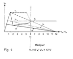
- FIG. 1 output characteristic curves are shown which show different courses of the output current I out due to a low-impedance load as a function of the source-drain voltage, ie the difference V bb - V out between the operating voltage V bb of the power transistor and that at the output connection , ie show output voltage V out dropping at a load with differently acting current limits.
- the solid characteristic curve a 1 shows the course of the output current I out achieved by the known current limitation
- the curve a 2 also drawn in solid lines, represents the current course when a load resistor is switched on in the circuit leading from the output connection of the power semiconductor switch to the load
- the dotted current curve b 1 represents a desired straight course of the current limitation
- the dotted current curve b 2 shows a current curve according to b 1 with the load resistor switched on.
- the dash-dotted curve c 1 represents a current curve when the current limitation is increased and the curve c 2 represents a current curve with the load resistor switched on when the current limitation is increased according to the curve c 1 .
- the current curve I out either - as the characteristic curve b 1 shows - takes a straight curve in which I out is essentially constant or even an increase according to the characteristic curve c 1 .
- the known current limiting circuit contains a current limiting branch for the voltage range above the threshold V s (6 V) of the differential voltage V bb - V out applied to the power semiconductor, and the drop shown by the current profile a 1 in FIG. 1 and the associated restriction of the Area of application below the threshold V s in purchase. So far, this has only been remedied by increasing the capacity of the charge pump. However, this can only be achieved by increasing the circuit area occupied by the charge pump and the drivers, the increased space requirement being disadvantageous in any case.
- the dip illustrated by the characteristic curve a 1 in FIG. 1 can be avoided with the charge pump unchanged.
- the first branch can be connected to the second branch when the voltage threshold V s is exceeded.
- the first branch is switched on and off by means of a depletion type N-channel field effect transistor. Its gate connection is due to a potential of V bb - Vs already present in the rest of the circuit, and its source connection is at the output connection of the power transistor. If the voltage V out at the output terminal is now higher than the gate potential V bb - Vs of the N-channel field effect transistor of the depletion type, a gate-source voltage U gs less than 0 is present at this transistor, the transistor pinches off, and the first branch the current limiting circuit is switched off. As a result, an output characteristic curve approximated to the current curve b 1 in FIG. 1 can be achieved.
- the exemplary embodiment of a power semiconductor switch according to the invention shown in the circuit diagram of FIG. 2 has the drain-source path of an N-channel power field effect transistor 1, which has a sense branch, in series with a load L which is connected to an output terminal (OUT) 4 is connected in parallel from an FET 2 and a shunt resistor 3.
- the drain connection of the FET 1 is connected to the operating voltage V bb , which, for. B. is 12 V.
- the gate connection G of the power FET 1 and the gate connection of the sense FET 2 are connected to a charge pump 5 via a rectifier 6 and a gate charging FET 7 functioning as a constant current source.
- the charge pump 5 supplies a direct current via the rectifier 6 and the constant current source 7, the strength of which depends on the capacitance, ie the strength of the charge pump 5 and the internal resistance R i which varies with the output voltage V out .
- Numeral 10 denotes a current limiting circuit which has three parallel branches 11, 12 and 13.
- the branch 11 (second branch) with a field effect transistor 14 has the function of limiting the current flowing through the load L and the FET 1 when the drain-source voltage V bb - V out of the FET 1 has a threshold value Vs (6 V ) falls below.
- this first branch 12 has a depletable N-channel field effect transistor 8 of the depletion type. Its gate connection is connected to a potential V bb - V s , V s being 6 V in the example in FIG. 2.
- the source connection of the N-channel field-effect transistor 8 is present at the output connection OUT 4, ie at the output voltage V out . If V out is now higher than the voltage difference V bb - V s , then a gate-source voltage U gs less than 0 is present at the field effect transistor 8, the transistor 8 pinches off and the first branch 12 is disconnected.
- Fig. 3 shows the improved achieved by branch 12 Output current characteristic d.
- a third parallel branch 13 to the current limiting circuit 10, the strength of which depends on the output voltage V out .
- An N-channel field-effect transistor 9 of the enhancement type lies in the third branch 13, the source connection of which lies at the output connection 4 and the gate connection of which is supplied with V bb .
- the gate connections of the field effect transistors 14, 15 and 16 in the branches 11, 12 and 13 of the current limiting circuit 10 are acted upon together with the potential falling across the shunt resistor 3.
Landscapes
- Electronic Switches (AREA)
- Emergency Protection Circuit Devices (AREA)
Abstract
Description
- Fig. 1
- verschiedene, vorangehend bereits beschriebene Ausgangskennlinien, d. h. Stromverläufe von überstrombegrenzten Leistungshalbleiterschaltern mit Ladungspumpe beim Schalten niederohmiger Lasten;
- Fig. 2
- ein schematisches Schaltbild eines Ausführungsbeispiels eines erfindungsgemäßen Leistungshalbleiterschalters; und
- Fig. 3
- Ausgangskennlinien, die mit der Strombegrenzung des in Fig. 2 dargestellten Ausführungsbeispiels des erfindungsgemäßen Leistungshalbleiterschalters erreichbar sind.
Die Gateanschlüsse der Feldeffekttransistoren 14, 15 und 16 in den Zweigen 11, 12 und 13 der Strombegrenzungsschaltung 10 sind gemeinsam mit dem am Shuntwiderstand 3 abfallenden Potenzial beaufschlagt.
Claims (8)
- Leistungshalbleiterschalter, insbesondere zum Schalten einer niederohmigen Last (L), mitdie Strombegrenzungsschaltung (10) einen ersten Zweig (12) aufweist für die Begrenzung des durch die Last (L) und den Leistungstransistor (1) fließenden Stroms (Iout), wenn die Drain-Source-Spannung des Leistungstransistors (1) einen bestimmten Spannungswert (Vs) überschreitet,einer zwischen dem Gateanschluss (G) eines Feldeffektleistungstransistors (1) und dessen an der Last (L) liegendem Ausgangsanschluss (4) eingeschalteten Strombegrenzungsschaltung (10) undeiner mit diesem Gateanschluss (G) verbundenen Ladungspumpe (5, 6, 7), mit der dem Gate (G) des Leistungstransistors (1) ein Ladestrom injiziert wird, wobei
dadurch gekennzeichnet, dass
die Strombegrenzungsschaltung (10) einen zweiten zum ersten Zweig (12) parallelen Zweig (11) für die Begrenzung des durch die Last (L) und den Leistungstransistor (1) fließenden Stroms (Iout) aufweist, wenn die Drain-Source-Spannung des Leistungstransistors (1) den bestimmten Wert (Vs) unterschreitet. - Leistungshalbleiterschalter nach Anspruch 1,
dadurch gekennzeichnet, dass
der erste Zweig (12) der Strombegrenzungsschaltung (10) einen abschnürbaren N-Kanal-Feldeffekttransistor (8) vom Verarmungstyp aufweist, durch den der erste Zweig (12) der Strombegrenzungsschaltung (10) dem zweiten Zweig (11) zuschaltbar ist, wenn die an der Last (L) abfallende bzw. am Ausgangsanschluss (4) liegende Ausgangsspannung (Vout) den bestimmten Spannungswert (Vs) unterschreitet und vom zweiten Zweig (11) der Strombegrenzungsschaltung (10) wegschaltbar ist, wenn die an der Last (L) abfallende bzw. am Ausgangsanschluss (4) liegende Spannung den bestimmten Spannungswert (Vs) überschreitet. - Leistungshalbleiterschalter nach Anspruch 2,
dadurch gekennzeichnet, dass
der Gateanschluss des N-Kanal-Feldeffekttransistors (8) mit einer Gatespannung beaufschlagt ist, die gleich der um den bestimmten Spannungswert (Vs) verminderten Betriebsspannung (Vbb) ist, und dass der Sourceanschluss des N-Kanal-Feldeffekttransistors (8) mit dem Sourceanschluss bzw. mit dem Ausgangsanschluss (4) des Leistungstransistors (1) verbunden ist. - Leistungshalbleiterschalter nach einem der Ansprüche 1 bis 3,
dadurch gekennzeichnet, dass
die Strombegrenzungsschaltung (10) außerdem einen dritten zum ersten und zweiten Zweig (12, 11) parallelen Zweig (13) aufweist, dessen Stärke von der an der Last (L) abfallenden bzw. am Ausgangsanschluss (4) anliegenden Spannung (Vout) abhängt. - Leistungshalbleiterschalter nach Anspruch 4,
dadurch gekennzeichnet, dass
der dritte Zweig (13) einen N-Kanal-Feldeffekttransistor (9) vom Anreicherungstyp aufweist, dessen Sourceanschluss mit dem Sourceanschluss des Leistungstransistors (1) verbunden und dessen Gateanschluss mit einem Teil der Betriebsspannung (Vbb) beaufschlagt ist. - Leistungshalbleiterschalter nach Anspruch 5,
dadurch gekennzeichnet, dass
der Gateanschluss des N-Kanal-Feldeffektransistors (9) mit einem mit höchstens dem bestimmten Spannungswert (Vs) gegen die an der Last (L) abfallende bzw. am Ausgangsanschluss (4) anliegende Ausgangsspannung (Vout) geklemmten Potenzial beaufschlagt ist. - Leistungshalbleiterschalter nach einem der vorangehenden Ansprüche,
dadurch gekennzeichnet, dass
er für eine Betriebsspannung Vbb = 12 V ausgelegt ist, und dass der bestimmte Spannungswert (Vs) 6 V beträgt. - Leistungshalbleiterschalter nach einem der vorangehenden Ansprüche,
dadurch gekennzeichnet, dass
außerdem in dem vom Sourcesanschluss des Leistungshalbleiters (1) zur Last (L) führenden Stromkreis ein zuschaltbarer Lastwiderstand vorgesehen ist.
Applications Claiming Priority (2)
| Application Number | Priority Date | Filing Date | Title |
|---|---|---|---|
| DE10038221 | 2000-08-04 | ||
| DE2000138221 DE10038221C2 (de) | 2000-08-04 | 2000-08-04 | Überstromgeschützter Halbleiterleistungsschalter, insbesondere zum Schalten niederohmiger Lasten |
Publications (2)
| Publication Number | Publication Date |
|---|---|
| EP1178606A2 true EP1178606A2 (de) | 2002-02-06 |
| EP1178606A3 EP1178606A3 (de) | 2005-04-06 |
Family
ID=7651406
Family Applications (1)
| Application Number | Title | Priority Date | Filing Date |
|---|---|---|---|
| EP01118563A Withdrawn EP1178606A3 (de) | 2000-08-04 | 2001-08-01 | Überstromgeschützter Halbleiterleistungsschalter, insbesondere zum Schalten niederohmiger Lasten |
Country Status (2)
| Country | Link |
|---|---|
| EP (1) | EP1178606A3 (de) |
| DE (1) | DE10038221C2 (de) |
Family Cites Families (6)
| Publication number | Priority date | Publication date | Assignee | Title |
|---|---|---|---|---|
| US4893158A (en) * | 1987-06-22 | 1990-01-09 | Nissan Motor Co., Ltd. | MOSFET device |
| US4808839A (en) * | 1988-04-04 | 1989-02-28 | Motorola, Inc. | Power field effect transistor driver circuit for protection from overvoltages |
| US5164659A (en) * | 1991-08-29 | 1992-11-17 | Warren Schultz | Switching circuit |
| US5272399A (en) * | 1992-02-25 | 1993-12-21 | Siemens Aktiengesellschaft | Circuit limiting the load current of a power MOSFET |
| DE19635332A1 (de) * | 1996-08-30 | 1998-03-12 | Siemens Ag | Leistungstransistor mit Kurzschluß-Schutz |
| DE69815010T2 (de) * | 1997-02-19 | 2004-02-12 | Koninklijke Philips Electronics N.V. | Leistungsvorrichtung mit kurzschlussdetektor |
-
2000
- 2000-08-04 DE DE2000138221 patent/DE10038221C2/de not_active Expired - Fee Related
-
2001
- 2001-08-01 EP EP01118563A patent/EP1178606A3/de not_active Withdrawn
Also Published As
| Publication number | Publication date |
|---|---|
| DE10038221A1 (de) | 2002-02-28 |
| EP1178606A3 (de) | 2005-04-06 |
| DE10038221C2 (de) | 2002-06-06 |
Similar Documents
| Publication | Publication Date | Title |
|---|---|---|
| DE19902520B4 (de) | Hybrid-Leistungs-MOSFET | |
| EP0557850B1 (de) | Schaltungsanordnung zur Laststrombegrenzung eines Leistungs-MOSFET | |
| DE102015102878B4 (de) | Elektronische Ansteuerschaltung | |
| DE102014108576B4 (de) | Treiberschaltung mit Miller-Clamping-Funktionalität für Leistungshalbleiterschalter, Leistungshalbleiterschalter und Wechselrichterbrücke | |
| EP0766395A2 (de) | Leistungstransistor mit Kurzschlussschutz | |
| DE102009007790B3 (de) | Treiberchip zum Treiben einer induktiven Last | |
| DE102010051874A1 (de) | Schaltung zum Schutz gegen Verpolung | |
| DE2639790C3 (de) | Schaltungsanordnung zur Lieferung konstanten Stroms | |
| DE4444623A1 (de) | Schaltungsanordnung zur Laststromregelung eines Leistungs-MOSFET | |
| DE4316275A1 (de) | MOS Leistungshalbleiter-Schalteinrichtung mit Lastkurzschlußschutz bei geringer Wärmeabfuhr | |
| DE2740763A1 (de) | Integrierte stromversorgungsschaltung | |
| DE102006041050B4 (de) | Schaltkreis mit zwei Mosfets | |
| DE102005005290A1 (de) | Konstantstromquellen-Vorrichtung mit zwei seriellen Verarmungs-MOS-Transistoren | |
| DE19838657B4 (de) | Schaltungsanordnung zum Erfassen des Laststromes eines Leistungs-Feldeffekt-Halbleiterbauelementes | |
| DE4403201C2 (de) | Ansteuerschaltung für ein MOS-Halbleiterbauelement mit sourceseitiger Last | |
| DE102005027442B4 (de) | Schaltungsanordnung zum Schalten einer Last | |
| EP0825716A2 (de) | Ansteuerschaltung für ein Feldeffekt gesteuertes Halbleiterbauelement | |
| DE10038221C2 (de) | Überstromgeschützter Halbleiterleistungsschalter, insbesondere zum Schalten niederohmiger Lasten | |
| EP0753754A2 (de) | Integrierte Komparatorschaltung | |
| DE20104111U1 (de) | Schaltungsanordnung zum Überstrom freien Ein- und Ausschalten eines Stromes | |
| DE19739999C2 (de) | Ansteuerschaltung für ein mittels Feldeffekt gesteuertes Leistungs-Halbleiterbauelement | |
| DE10349629B4 (de) | Elektronischer Schaltkreis | |
| DE60126191T2 (de) | CMOS Bustreiber | |
| DE19547768C1 (de) | Elektrische Schaltvorrichtung | |
| DE19547778C1 (de) | CMOS-Treiberschaltung |
Legal Events
| Date | Code | Title | Description |
|---|---|---|---|
| PUAI | Public reference made under article 153(3) epc to a published international application that has entered the european phase |
Free format text: ORIGINAL CODE: 0009012 |
|
| AK | Designated contracting states |
Kind code of ref document: A2 Designated state(s): AT BE CH CY DE DK ES FI FR GB GR IE IT LI LU MC NL PT SE TR |
|
| AX | Request for extension of the european patent |
Free format text: AL;LT;LV;MK;RO;SI |
|
| PUAL | Search report despatched |
Free format text: ORIGINAL CODE: 0009013 |
|
| AK | Designated contracting states |
Kind code of ref document: A3 Designated state(s): AT BE CH CY DE DK ES FI FR GB GR IE IT LI LU MC NL PT SE TR |
|
| AX | Request for extension of the european patent |
Extension state: AL LT LV MK RO SI |
|
| 17P | Request for examination filed |
Effective date: 20050928 |
|
| AKX | Designation fees paid |
Designated state(s): DE FR IT |
|
| 17Q | First examination report despatched |
Effective date: 20060808 |
|
| STAA | Information on the status of an ep patent application or granted ep patent |
Free format text: STATUS: THE APPLICATION IS DEEMED TO BE WITHDRAWN |
|
| 18D | Application deemed to be withdrawn |
Effective date: 20080303 |