EP1178539A2 - Schottky field-effect transistor - Google Patents
Schottky field-effect transistor Download PDFInfo
- Publication number
- EP1178539A2 EP1178539A2 EP01113993A EP01113993A EP1178539A2 EP 1178539 A2 EP1178539 A2 EP 1178539A2 EP 01113993 A EP01113993 A EP 01113993A EP 01113993 A EP01113993 A EP 01113993A EP 1178539 A2 EP1178539 A2 EP 1178539A2
- Authority
- EP
- European Patent Office
- Prior art keywords
- trench
- effect transistor
- substrate
- schottky
- transistor switch
- Prior art date
- Legal status (The legal status is an assumption and is not a legal conclusion. Google has not performed a legal analysis and makes no representation as to the accuracy of the status listed.)
- Withdrawn
Links
- 230000005669 field effect Effects 0.000 title claims abstract description 24
- 239000000758 substrate Substances 0.000 claims abstract description 41
- 229910052751 metal Inorganic materials 0.000 claims abstract description 24
- 239000002184 metal Substances 0.000 claims abstract description 24
- 239000004065 semiconductor Substances 0.000 claims abstract description 17
- 238000000034 method Methods 0.000 claims description 18
- 239000002019 doping agent Substances 0.000 claims description 15
- 229910021420 polycrystalline silicon Inorganic materials 0.000 claims description 15
- 229920005591 polysilicon Polymers 0.000 claims description 15
- 230000004888 barrier function Effects 0.000 claims description 11
- 239000004020 conductor Substances 0.000 claims description 9
- 230000015556 catabolic process Effects 0.000 claims description 7
- RTAQQCXQSZGOHL-UHFFFAOYSA-N Titanium Chemical compound [Ti] RTAQQCXQSZGOHL-UHFFFAOYSA-N 0.000 claims description 3
- 238000004519 manufacturing process Methods 0.000 claims description 3
- 239000010936 titanium Substances 0.000 claims description 3
- 229910052719 titanium Inorganic materials 0.000 claims description 3
- 238000005520 cutting process Methods 0.000 claims description 2
- 229910021341 titanium silicide Inorganic materials 0.000 claims description 2
- 238000000151 deposition Methods 0.000 claims 4
- PXHVJJICTQNCMI-UHFFFAOYSA-N Nickel Chemical compound [Ni] PXHVJJICTQNCMI-UHFFFAOYSA-N 0.000 claims 2
- 238000005530 etching Methods 0.000 claims 1
- 229910052759 nickel Inorganic materials 0.000 claims 1
- RUFLMLWJRZAWLJ-UHFFFAOYSA-N nickel silicide Chemical compound [Ni]=[Si]=[Ni] RUFLMLWJRZAWLJ-UHFFFAOYSA-N 0.000 claims 1
- 229910021334 nickel silicide Inorganic materials 0.000 claims 1
- 230000005684 electric field Effects 0.000 abstract description 8
- 238000009825 accumulation Methods 0.000 abstract description 7
- 239000000463 material Substances 0.000 abstract description 6
- 230000000694 effects Effects 0.000 description 5
- ZOXJGFHDIHLPTG-UHFFFAOYSA-N Boron Chemical compound [B] ZOXJGFHDIHLPTG-UHFFFAOYSA-N 0.000 description 4
- 229910052796 boron Inorganic materials 0.000 description 4
- 229910052581 Si3N4 Inorganic materials 0.000 description 3
- XUIMIQQOPSSXEZ-UHFFFAOYSA-N Silicon Chemical compound [Si] XUIMIQQOPSSXEZ-UHFFFAOYSA-N 0.000 description 3
- 230000007423 decrease Effects 0.000 description 3
- 229910052710 silicon Inorganic materials 0.000 description 3
- 239000010703 silicon Substances 0.000 description 3
- HQVNEWCFYHHQES-UHFFFAOYSA-N silicon nitride Chemical compound N12[Si]34N5[Si]62N3[Si]51N64 HQVNEWCFYHHQES-UHFFFAOYSA-N 0.000 description 3
- OAICVXFJPJFONN-UHFFFAOYSA-N Phosphorus Chemical compound [P] OAICVXFJPJFONN-UHFFFAOYSA-N 0.000 description 2
- VYPSYNLAJGMNEJ-UHFFFAOYSA-N Silicium dioxide Chemical group O=[Si]=O VYPSYNLAJGMNEJ-UHFFFAOYSA-N 0.000 description 2
- 230000000903 blocking effect Effects 0.000 description 2
- 210000000746 body region Anatomy 0.000 description 2
- 238000001312 dry etching Methods 0.000 description 2
- 238000001465 metallisation Methods 0.000 description 2
- 150000004767 nitrides Chemical class 0.000 description 2
- 229910052698 phosphorus Inorganic materials 0.000 description 2
- 239000011574 phosphorus Substances 0.000 description 2
- 230000001681 protective effect Effects 0.000 description 2
- 238000000137 annealing Methods 0.000 description 1
- 229910052785 arsenic Inorganic materials 0.000 description 1
- RQNWIZPPADIBDY-UHFFFAOYSA-N arsenic atom Chemical compound [As] RQNWIZPPADIBDY-UHFFFAOYSA-N 0.000 description 1
- 230000015572 biosynthetic process Effects 0.000 description 1
- 239000000969 carrier Substances 0.000 description 1
- 230000001413 cellular effect Effects 0.000 description 1
- 230000003247 decreasing effect Effects 0.000 description 1
- 230000007547 defect Effects 0.000 description 1
- 230000001419 dependent effect Effects 0.000 description 1
- 238000010586 diagram Methods 0.000 description 1
- 239000007943 implant Substances 0.000 description 1
- 238000002513 implantation Methods 0.000 description 1
- 238000002347 injection Methods 0.000 description 1
- 239000007924 injection Substances 0.000 description 1
- 150000002500 ions Chemical class 0.000 description 1
- 230000003647 oxidation Effects 0.000 description 1
- 238000007254 oxidation reaction Methods 0.000 description 1
- 229920002120 photoresistant polymer Polymers 0.000 description 1
- 235000012239 silicon dioxide Nutrition 0.000 description 1
- 239000000377 silicon dioxide Substances 0.000 description 1
- 238000004088 simulation Methods 0.000 description 1
- WFKWXMTUELFFGS-UHFFFAOYSA-N tungsten Chemical compound [W] WFKWXMTUELFFGS-UHFFFAOYSA-N 0.000 description 1
- 229910052721 tungsten Inorganic materials 0.000 description 1
- 239000010937 tungsten Substances 0.000 description 1
- WQJQOUPTWCFRMM-UHFFFAOYSA-N tungsten disilicide Chemical compound [Si]#[W]#[Si] WQJQOUPTWCFRMM-UHFFFAOYSA-N 0.000 description 1
- 229910021342 tungsten silicide Inorganic materials 0.000 description 1
Images


Classifications
-
- H—ELECTRICITY
- H01—ELECTRIC ELEMENTS
- H01L—SEMICONDUCTOR DEVICES NOT COVERED BY CLASS H10
- H01L29/00—Semiconductor devices specially adapted for rectifying, amplifying, oscillating or switching and having potential barriers; Capacitors or resistors having potential barriers, e.g. a PN-junction depletion layer or carrier concentration layer; Details of semiconductor bodies or of electrodes thereof ; Multistep manufacturing processes therefor
- H01L29/66—Types of semiconductor device ; Multistep manufacturing processes therefor
- H01L29/86—Types of semiconductor device ; Multistep manufacturing processes therefor controllable only by variation of the electric current supplied, or only the electric potential applied, to one or more of the electrodes carrying the current to be rectified, amplified, oscillated or switched
- H01L29/861—Diodes
- H01L29/872—Schottky diodes
- H01L29/8725—Schottky diodes of the trench MOS barrier type [TMBS]
-
- H—ELECTRICITY
- H01—ELECTRIC ELEMENTS
- H01L—SEMICONDUCTOR DEVICES NOT COVERED BY CLASS H10
- H01L29/00—Semiconductor devices specially adapted for rectifying, amplifying, oscillating or switching and having potential barriers; Capacitors or resistors having potential barriers, e.g. a PN-junction depletion layer or carrier concentration layer; Details of semiconductor bodies or of electrodes thereof ; Multistep manufacturing processes therefor
- H01L29/66—Types of semiconductor device ; Multistep manufacturing processes therefor
- H01L29/66007—Multistep manufacturing processes
- H01L29/66075—Multistep manufacturing processes of devices having semiconductor bodies comprising group 14 or group 13/15 materials
- H01L29/66227—Multistep manufacturing processes of devices having semiconductor bodies comprising group 14 or group 13/15 materials the devices being controllable only by the electric current supplied or the electric potential applied, to an electrode which does not carry the current to be rectified, amplified or switched, e.g. three-terminal devices
- H01L29/66409—Unipolar field-effect transistors
- H01L29/66477—Unipolar field-effect transistors with an insulated gate, i.e. MISFET
- H01L29/66666—Vertical transistors
-
- H—ELECTRICITY
- H01—ELECTRIC ELEMENTS
- H01L—SEMICONDUCTOR DEVICES NOT COVERED BY CLASS H10
- H01L29/00—Semiconductor devices specially adapted for rectifying, amplifying, oscillating or switching and having potential barriers; Capacitors or resistors having potential barriers, e.g. a PN-junction depletion layer or carrier concentration layer; Details of semiconductor bodies or of electrodes thereof ; Multistep manufacturing processes therefor
- H01L29/66—Types of semiconductor device ; Multistep manufacturing processes therefor
- H01L29/68—Types of semiconductor device ; Multistep manufacturing processes therefor controllable by only the electric current supplied, or only the electric potential applied, to an electrode which does not carry the current to be rectified, amplified or switched
- H01L29/70—Bipolar devices
- H01L29/72—Transistor-type devices, i.e. able to continuously respond to applied control signals
- H01L29/739—Transistor-type devices, i.e. able to continuously respond to applied control signals controlled by field-effect, e.g. bipolar static induction transistors [BSIT]
- H01L29/7391—Gated diode structures
-
- H—ELECTRICITY
- H01—ELECTRIC ELEMENTS
- H01L—SEMICONDUCTOR DEVICES NOT COVERED BY CLASS H10
- H01L29/00—Semiconductor devices specially adapted for rectifying, amplifying, oscillating or switching and having potential barriers; Capacitors or resistors having potential barriers, e.g. a PN-junction depletion layer or carrier concentration layer; Details of semiconductor bodies or of electrodes thereof ; Multistep manufacturing processes therefor
- H01L29/66—Types of semiconductor device ; Multistep manufacturing processes therefor
- H01L29/68—Types of semiconductor device ; Multistep manufacturing processes therefor controllable by only the electric current supplied, or only the electric potential applied, to an electrode which does not carry the current to be rectified, amplified or switched
- H01L29/76—Unipolar devices, e.g. field effect transistors
- H01L29/772—Field effect transistors
- H01L29/78—Field effect transistors with field effect produced by an insulated gate
- H01L29/7827—Vertical transistors
- H01L29/7828—Vertical transistors without inversion channel, e.g. vertical ACCUFETs, normally-on vertical MISFETs
-
- H—ELECTRICITY
- H01—ELECTRIC ELEMENTS
- H01L—SEMICONDUCTOR DEVICES NOT COVERED BY CLASS H10
- H01L29/00—Semiconductor devices specially adapted for rectifying, amplifying, oscillating or switching and having potential barriers; Capacitors or resistors having potential barriers, e.g. a PN-junction depletion layer or carrier concentration layer; Details of semiconductor bodies or of electrodes thereof ; Multistep manufacturing processes therefor
- H01L29/66—Types of semiconductor device ; Multistep manufacturing processes therefor
- H01L29/68—Types of semiconductor device ; Multistep manufacturing processes therefor controllable by only the electric current supplied, or only the electric potential applied, to an electrode which does not carry the current to be rectified, amplified or switched
- H01L29/76—Unipolar devices, e.g. field effect transistors
- H01L29/772—Field effect transistors
- H01L29/78—Field effect transistors with field effect produced by an insulated gate
- H01L29/7839—Field effect transistors with field effect produced by an insulated gate with Schottky drain or source contact
-
- H—ELECTRICITY
- H01—ELECTRIC ELEMENTS
- H01L—SEMICONDUCTOR DEVICES NOT COVERED BY CLASS H10
- H01L29/00—Semiconductor devices specially adapted for rectifying, amplifying, oscillating or switching and having potential barriers; Capacitors or resistors having potential barriers, e.g. a PN-junction depletion layer or carrier concentration layer; Details of semiconductor bodies or of electrodes thereof ; Multistep manufacturing processes therefor
- H01L29/66—Types of semiconductor device ; Multistep manufacturing processes therefor
- H01L29/86—Types of semiconductor device ; Multistep manufacturing processes therefor controllable only by variation of the electric current supplied, or only the electric potential applied, to one or more of the electrodes carrying the current to be rectified, amplified, oscillated or switched
- H01L29/861—Diodes
- H01L29/872—Schottky diodes
Definitions
- This invention relates to semiconductor switches.
- MOSFETs Semiconductor switches, typically MOSFETs, are widely used to control the flow of power to electronic devices such as computers and cellular telephones.
- the supply voltage at which these devices operate is decreasing rapidly ⁇ from 5 V to 3.3 V and below. It is likely that supply voltages will drop to 1 V or less within the foreseeable future.
- the challenge is to develop power switches that can be switched on and off with a control signal of 1 V or less and that have a very low forward voltage drop when they are conducting. It is impossible to lower the threshold voltage of a conventional enhancement-mode power MOSFET below 0.5 V without creating an excessive leakage current when the device is turned off; and a conventional MOSFET with a threshold voltage of 0.5 V or more cannot be fully turned on unless the gate voltage is greater than 1.5 V.
- Depletion mode MOSFETs have a restricted current capability and the use of bipolar transistors as switches is limited by the need to provide a continuous base current.
- a Schottky diode is connected in series with the power switch to protect the circuitry against a reverse bias condition.
- the forward voltage drop across the Schottky diode creates a further power loss and reduces the efficiency of the system.
- the voltage drop across the Schottky diode should be much less than the supply voltage.
- the Barrier-ACCUFET 150 includes trenches 1502 formed in a semiconductor substrate 1504.
- a gate 1506 is located in the trenches 1502, insulated by a dielectric layer 1508 from the substrate 1504.
- Substrate 1504 also includes a heavily-doped N+ region 1510 and an N- drift region 1512, which together form the drain of the device.
- a P-body 1514 and N+ source regions 1516 are formed near the surface of the substrate 1504.
- the gate 1506 is doped with N-type material, creating charge depletion regions in the N- drift region 1512.
- the parameters of the device are set to ensure that these depletion regions merge at the center of the mesa between the trenches when the gate is biased off, as shown in Fig. 15A , pinching off the current flow between the N+ source regions 1516 and the N+ region 1510.
- the electric field emanating from the gate is used to shield the P body against the punchthrough phenomenon.
- the charge density of the dopant in the portion of the N- drift region 1512 that is located in the mesa calculated as an integral of the net doping concentration across the width of the mesa, is less than 5 x 10 12 cm -2 .
- the two-dimensional pinching effect caused by the gate electrodes and the junction between P body 1514 and N- drift region 1512 allows the net charge density in the P body region to be much lower than in conventional trench MOSFETs. This in turn sllows a design of a MOSFET with a short channel and a low threshold voltage while maintaining a reasonable thickness of the dielectric layer 1508, which is typically an oxide.
- Fig. 15B when the gate voltage of the Barrier-ACCUFET is increased, the depletion regions surrounding the trench contract, and accumulation regions 1518 are formed in the N- drift region 1512 adjacent to the trench. Accumulation regions 1518 provide a low-resistance current path between the N+ source regions 1516 and the drain, and reduce the voltage drop across the device in a conduction mode.
- a deep trench reaching the N+ substrate _ is used to minimize the on-resistance of the switch, and the portion of the dielectric layer 1508 at the bottom of the trench is made thicker to reduce the strength of the electric field at the bottom comer of the trench.
- the strength of the electric field normally reaches a maximum at this comer, and the dielectric layer there is particularly vulnerable to damage from impact ionization and hot carrier generation.
- TMBS-diode Trench-MOS-Barrier Schottky diode
- a TMBS-diode is described, for example, in U.S. Patent No. 5,365,102 to Mehtrota et al. and U.S. Application No. 08/832,012, now U.S. Patent No. 5,XXX,XXX, to Williams et al.
- a major disadvantage of a Schottky diode is its relatively high reverse leakage current, which is typically orders of magnitude higher than the reverse leakage of a PN junction diode. Moreover, the leakage current in a Schottky diode is strongly dependent on the magnitude of the reverse voltage, as a consequence of reverse-voltage-induced barrier-lowering at the rectifying metal-semiconductor interface (sometimes referred to as a "Schottky-barrier"). Unfortunately, using a metal which has a large Schottky barrier height and thereby reducing the leakage current increase the forward voltage drop across the diode. This leads to a difficult trade-off between the forward and reverse bias characteristics of the diode.
- TMBS-diode reduces the trade-off between forward voltage drop and reverse leakage current by taking advantage of a pinching effect similar to that described above in connection with the Barrier-ACCUFET.
- Figs. 16A and 16B show cross-sectional views of a TMBS-diode 160 in the off- and on-states, respectively.
- TMBS-diode 160 is formed in an N+ substrate 1602 and an N- layer 1604.
- the gate electrodes 1606 are located in trenches 1608 which form a mesa between them.
- the Schottky interface is between the top surface of N- layer 1604 and a Schottky metal 1610. Schottky metal 1610 is connected to the gate electrodes 1606. As shown in Fig.
- the high electric field appearing at the bottom comer of the trench can lead to severe reliability problems by charging the gate dielectric layer 1612 with hot carriers.
- this problem can be alleviated somewhat by introducing a deep PN junction with a breakdown voltage lower than that of the trench structure.
- a Schottky field-effect transistor (SFET) switch in accordance with this invention is formed in a semiconductor substrate having first and second trench segments separated by a mesa.
- a metal layer forming a Schottky interface is formed on the surface of the mesa.
- the metal layer and the substrate represent the anode and cathode terminals, respectively, of the switch.
- a conductive material in the trench segments forms a gate electrode, the gate electrode being insulated by a dielectric layer from the semiconductor substrate and the metal layer.
- the substrate is generally doped with N-type dopant, and the conductive material which forms the gate electrode is also doped with N-type dopant. This creates depletion regions in the mesa which can merge to pinch off current between the anode and the cathode.
- the SFET switch is controlled by the voltage on the gate.
- the gate When the gate is biased positive, accumulation regions form along the walls of the trench and a current can flow from the anode layer to the cathode.
- the gate When the gate is biased negative, the depletion regions expand, choking off practically any current between the anode and cathode terminals. For example, if the anode is biased at 1 V and the cathode is grounded, a voltage of 1 V applied to the gate produces a forward voltage drop of less than 0.3 V at 100 A/cm 2 and room temperature. On the other hand, a voltage of-1 V applied to the gate reduces the forward anode current to less than 1 mA/mm 2 .
- the switch blocks current independent of the gate bias. Applying a positive or negative voltage to the gate increases or decreases the current, respectively, by a factor of two or three. If the absolute value of the negative blocking gate voltage is larger than the reverse bias applied to the switch, the leakage current can be suppressed by more than two orders of magnitude.
- the SFET switch of this invention is thus ideally suited to use with low supply voltages of, for example, 1 V or less.
- the switch can also be formed in a P-type substrate, in which case the polarities of the gate dopant and voltages are reversed.
- the SFET switch may be formed in a substrate which includes a lightly doped epitaxial layer grown on a heavily doped semiconductor piece.
- the trench extends through the epitaxial layer into the heavily doped material.
- the dielectric layer may be made thicker at the bottom of the trench.
- a PN clamping diode may be formed integrally in parallel with the trench structure to prevent damage to the dielectric layer from high electric fields. The clamped diode is designed to have a breakdown voltage that is less than a voltage that would damage the dielectric layer.
- Figs. 1A and 1B show cross-sectional views of a Schottky field-effect transistor (SFET) switch 10 in accordance with this invention.
- Fig. 1A shows switch 10 in a current-blocking state;
- Fig. 1B shows switch 10 in a conductive state.
- the switch is formed in a silicon substrate 102 which includes a heavily doped N+ piece 104 on which a lightly doped N- epitaxial (epi) layer or drift region 106 is grown.
- N+ piece 104 is generally doped with arsenic to a doping concentration of about 2 x 10 19 cm -3 .
- a trench 108 which includes segments 108A and 108B is formed in substrate 102, the trench segments being separated by a mesa 110.
- a metal layer 112 is deposited on the substrate 102 and forms a rectifying Schottky interface 114 with the top surface of mesa 110.
- Each of trench segments 108A and 108B (sometimes referred to collectively as trenches 108) contains a conductive gate material, in this case polysilicon, which is doped with N-type dopant, typically phosphorus.
- the polysilicon gate is insulated from the substrate 102 and the metal layer 112 by a dielectric layer 118, which in this embodiment is silicon dioxide.
- dielectric layer 118 includes thin portions adjacent the side walls of the trenches 108 and thicker portions 118A and 118B at the top and bottom of the trenches, respectively.
- Metal layer 112 represents the anode and N+ region 104 represents the cathode of SFET switch 10.
- a metal cathode contact (not shown) would typically be formed on the back side of N+ region 104, although in some embodiments the cathode is contacted by an N+ sinker extending from the front side of the substrate. Since switch 10 is an N-type device, the metal in layer could be titanium, the barrier at the metal-semiconductor Schottky interface 114 is 0.51 eV. Gate 116 is typically contacted somewhere in the third dimension, outside the plane of the paper.
- the mesa between trenches 108 can take many shapes, e.g., rectangular, square, hexagonal, or longitudinal stripes, and the trenches are connected together in a lattice which defines numerous mesas or "cells", all of which are connected in parallel.
- the Schottky interface 114 When the anode is biased positive with respect to the cathode, the Schottky interface 114 is forward-biased, and current flow through the N- drift region 106 is controlled by the lateral electric field generated by the gate electrode 116.
- the gate electrode 116 can be connected directly to the metal layer 112 (i.e., the gate is shorted to the anode). In this mode the device operates like the TMBS-diode described in the above-referenced U.S. Patent No. 5,XXX,XXX to Williams et al.
- the accumulation layer provides a very low-resistance path, so only the barrier represented by the Schottky interface 114 needs to be overcome. This yields a very low voltage drop for the device.
- the normally leaky Schottky interface is supported by the pinching effect of the electric field generated by the gate electrodes.
- the Schottky interface 114 is reverse-biased, and a substantial current will not flow regardless of how the gate is biased. Applying a bias to the gate, however, can increase or reduce the leakage current by a factor of 2 or 3. If the gate is biased positively, the leakage current increases; if the gate is biased negatively, the leakage current decreases. If the gate is biased negative at a level greater than the reverse bias on the anode-cathode terminals of switch 10, however, the leakage current is suppressed by more than two orders of magnitude.
- the Schottky diode With its ultra-low forward voltage drop, defines the forward and reverse characteristics of the device which are similar to those of a TMBS-diode.
- the reverse characteristic is a flat, voltage-independent leakage current; this is due to the pinching effect of the field generated by the gate.
- Forward biasing the gate electrode with respect to the cathode in the conduction mode (V A > V G > V C ) further reduces the resistance of the device in the conduction mode.
- Applying a reverse bias to the gate in the conduction mode results in a blocking of the current.
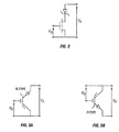
- Fig. 2 The behavior of the device is somewhat similar to that of a serial connection of a Schottky diode and a depletion mode MOSFET, shown in Fig. 2.
- Figs. 3A and 3B show proposed symbols for the SFET fabricated using N-type and P-type substrates, respectively.
- a P-type region 120 is formed in substrate 102 by implantation outside mesa 110. Region forms a PN junction 122 with the remaining N-type portion of substrate 102, which represents a clamping diode that at a desired voltage to protect the trench structure and in particular prevent the field strength from reaching the point at which hot carrier injection into the gate dielectric layer 118 occurs.
- the technique of doping P region 120 to provide a desired breakdown voltage at junction 122 is well known (see, e.g., Sze, Physics of Semiconductor Devices, 2 nd Ed., John Wiley & Sons (1981), pp. 96-109, incorporated herein by reference).
- the distance between trenches 108 (which is also the width W of mesa 110, see Fig. 1A ) is preferably less than 1.2 ⁇ m and more preferably between 0.4 and 0.6 ⁇ m.
- the doping concentration in the drift region 106 is preferably less than 1 x 10 16 cm -3 . Normally, the doping concentration in N-epi layer 106 will actually be graduated, with the concentration increasing gradually with distance from the surface of layer 106 to a relatively sharp increase at the junction between N-epi layer 106 and the N+ piece 104.
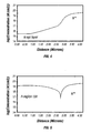
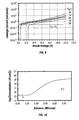
- Fig. 4 is graph of the doping concentration in a vertical cross-section 4-4 through mesa 110 in one embodiment
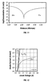
- Fig. 5 is a graph of the doping concentration in a vertical cross-section 5-5 through P-region 120 in the same embodiment.
- a SFET switch can be manufactured by any one of several known process flows for making trench MOSFETs. There are several differences, however, including: (a) no source or body regions are formed; (b) the metallization scheme used on the top surface of the substrate should result in a Schottky interface with a low barrier height, preferably below 0.6 eV and more preferably around 0.5 eV.
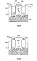
- Figs. 6A and 6B illustrate the steps of one process for manufacturing SFET 10 shown in Fig. 1.
- N- epi layer 106 is grown on an N+ silicon piece 104 using a known type of epitaxial reactor.
- Epi layer 106 may include two or more sublayers; in this embodiment, an upper sublayer is 3.7 ⁇ m thick and has an average doping concentration of 2 x 10 15 cm -3 and a lower sublayer is 0.5 ⁇ m thick and has an average doping concentration of 3 x 10 17 cm -3 .
- a thin pad oxide layer 602 and a silicon nitride layer 604 are formed on the top surface of epi layer 106 and patterned with openings where the trenches 108 are to be located.
- pad oxide layer 602 can be 30 nm thick and silicon nitride layer 604 can be 150 nm thick.
- Trenches 108 are formed by cutting through epi layer to the N+ silicon, preferably by dry-etching. A sacrificial oxide layer is grown on the walls of the trenches and etched back to eliminate any defects caused during the formation of the trenches.
- trenches 108 are 0.8 ⁇ m wide and 2.2 ⁇ m deep and are separated laterally by 0.4 ⁇ m.
- gate oxide layer 118 is thermally grown on the side walls and floor of the trenches.
- the thicker portion 118B can be formed in the lower portion of the trenches 108 by the techniques described in U.S. Patent No. 4,914,058 to Blanchard, issued April 3, 1990, and in Application No. [Attorney Docket No. M-8200 US] , by Giles et al., filed June 8, 2000, both of which are incorporated herein by reference.
- the thicker portion of the dielectric layer may include a polysilicon plug as taught in the above-referenced Application No. [Attorney Docket No. M-8200] and in Application No. [Attorney Docket No.
- the thickness of the oxide layer 118 on the walls of the trenches can be 50 nm and the thickness of the thicker portion 118B can be 200 nm, for example.
- Polysilicon is deposited in the trenches and etched back to a level below the surface of epi layer 106 to form gate electrodes 116.
- the polysilicon is doped with N-type material to a concentration of 10 19 cm -3 , for example.
- the etchback of the polysilicon leaves at recess 606 which can be 0.1 ⁇ m deep.
- the exposed polysilicon is thermally oxidized to an oxide thickness of 0.2 ⁇ m, for example, to yield thicker portions 118A and a generally flat topology on the top surface of the structure.
- the silicon nitride layer 604 and pad oxide layer 602 are removed with conventional etchants, yielding a self-aligned definition of the contact areas.
- contact windows to the gate are opened through the thicker portions 118A, using a dedicated mask and a dry-etching (reactive ion etch) process. Referring to Figs.
- metal layer 112 is then deposited on the top surface of the mesa 110 and the thicker oxide portion 118A to form the Schottky interface 114. Because of the high doping concentration of the polysilicon gate, metal layer 112 forms an ohmic contact with the polysilicon at the locations of the gate contact windows. Metal layer 114 is patterned using a photoresist mask to form anode and gate electrodes. A metal layer (not shown) is deposited on the back side of the N+ substrate to form an ohmic contact to the cathode.
- a preferred metal for layer 112 is titanium, which produces a Schottky barrier of 0.51 eV, but other materials such as titanium silicide, tungsten or tungsten silicide could also be used.
- the structure can be masked before pad oxide layer 602 and nitride layer 604 are formed, and a P-type dopant such as boron is implanted at a dose of 8 x 10 15 cm -2 and an energy of 80 keV.
- the implanted dopant can be driven in at 1050 °C for 60 minutes and 950 °C for 130 minutes to form P-region 120, having an average doping concentration of about 10 19 cm -3 .
- SFET 10 shown in Fig. 1.
- the doping profiles of the mesa 110 and P-region 120 are shown in Figs. 4 and 5, respectively.
- the resulting breakdown voltage of the trench structure was about 18 V, and the clamping diode had a breakdown voltage of about 12 V.
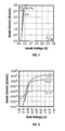
- Fig. 8 is a graph on semilog paper of the anode current density of SFET 10 as V G swings between +1 V and -1 V for several values of V A .
- V A is equal to 1 V the current density varies between 20 A/mm 2 and 0.3 mA/mm 2 as V G varies between +1 V and -1 V.
- the SFET is an ideal power switch for operation in the voltage range below 3 V.
- advantages of the SFET are the following:
- Fig. 9 is a graph on semilog paper of the simulated reverse characteristics of SFET 10, showing the leakage current density as a function of V A for various values of V G .
- This graph clearly indicates that the leakage current can be reduced to essentially zero by applying a V G that is greater than V A , in absolute terms, i.e.,
- Table 1 shows the design parameters of an illustrative P-type SFET.
- Epi layer structure Upper sublayer: 4.3 ⁇ m, 2 x 10 15 cm -3 , boron Lower sublayer: 1.5 ⁇ m, 3 x 10 17 cm -3 , boron Surface doping dose 1 x 10 11 cm -2 @ 40 keV (BF 2 implanted through gate oxide)
- the shallow BF 2 implant is used to define the doping concentration at the surface of the epi layer to compensate for the effect of boron redistribution at the top surface during thermal oxidation and annealing processes.
- the BF 2 is implanted through the gate oxide, which at this point covers the top surface of the mesa.
- Fig. 10 shows the doping concentration in a vertical section through the mesa and Fig. 11 shows the doping concentration through the clamping diode.
- Fig. 10 it is evident that the dopant from the lower epi sublayer has outdiffused, increasing the doping concentration of the lower part of the upper epi sublayer.
- Figs. 12-14 are graphs showing the simulated characteristic of the P-type SFET characterized in Table 1.
- Fig. 13 is a graph on semilog paper of the anode current density of the P-type SFET 10 V G swings between +1 V and -1 V for several values of V A .
- V A is equal to 1 V the current density varies between 10 A/mm 2 and less than 1mA/mm 2 as V G varies between -1 V and +1 V.
- Fig. 14 is a graph on semilog paper of the simulated reverse characteristics of SFET 10, showing the leakage current density as a function of V A for various values of V G .
Landscapes
- Engineering & Computer Science (AREA)
- Microelectronics & Electronic Packaging (AREA)
- Power Engineering (AREA)
- Physics & Mathematics (AREA)
- Ceramic Engineering (AREA)
- Condensed Matter Physics & Semiconductors (AREA)
- General Physics & Mathematics (AREA)
- Computer Hardware Design (AREA)
- Manufacturing & Machinery (AREA)
- Junction Field-Effect Transistors (AREA)
- Electrodes Of Semiconductors (AREA)
Abstract
Description
- This invention relates to semiconductor switches.
- Semiconductor switches, typically MOSFETs, are widely used to control the flow of power to electronic devices such as computers and cellular telephones. The supply voltage at which these devices operate is decreasing rapidly―from 5 V to 3.3 V and below. It is likely that supply voltages will drop to 1 V or less within the foreseeable future.
- To accommodate this decrease in supply voltage, the challenge is to develop power switches that can be switched on and off with a control signal of 1 V or less and that have a very low forward voltage drop when they are conducting. It is impossible to lower the threshold voltage of a conventional enhancement-mode power MOSFET below 0.5 V without creating an excessive leakage current when the device is turned off; and a conventional MOSFET with a threshold voltage of 0.5 V or more cannot be fully turned on unless the gate voltage is greater than 1.5 V. Depletion mode MOSFETs have a restricted current capability and the use of bipolar transistors as switches is limited by the need to provide a continuous base current.
- Furthermore, in many applications a Schottky diode is connected in series with the power switch to protect the circuitry against a reverse bias condition. When this is done, the forward voltage drop across the Schottky diode creates a further power loss and reduces the efficiency of the system. To prevent this from being a significant power dissipation factor, the voltage drop across the Schottky diode should be much less than the supply voltage.
- Application No 09/476,320 describes a Barrier Accumulation-Mode Field-Effect Transistor (Barrier-ACCUFET), a cross-sectional view of which is shown in Figs. 15A and 15B. The Barrier-ACCUFET 150 includes
trenches 1502 formed in asemiconductor substrate 1504. Agate 1506 is located in thetrenches 1502, insulated by adielectric layer 1508 from thesubstrate 1504.Substrate 1504 also includes a heavily-dopedN+ region 1510 and an N-drift region 1512, which together form the drain of the device. A P-body 1514 andN+ source regions 1516 are formed near the surface of thesubstrate 1504. Thegate 1506 is doped with N-type material, creating charge depletion regions in the N-drift region 1512. The parameters of the device are set to ensure that these depletion regions merge at the center of the mesa between the trenches when the gate is biased off, as shown in Fig. 15A, pinching off the current flow between theN+ source regions 1516 and theN+ region 1510. The electric field emanating from the gate is used to shield the P body against the punchthrough phenomenon. To ensure that the depletion regions merge, the charge density of the dopant in the portion of the N-drift region 1512 that is located in the mesa, calculated as an integral of the net doping concentration across the width of the mesa, is less than 5 x 1012 cm-2. - The two-dimensional pinching effect caused by the gate electrodes and the junction between
P body 1514 and N-drift region 1512 allows the net charge density in the P body region to be much lower than in conventional trench MOSFETs. This in turn sllows a design of a MOSFET with a short channel and a low threshold voltage while maintaining a reasonable thickness of thedielectric layer 1508, which is typically an oxide. - As shown in Fig. 15B, when the gate voltage of the Barrier-ACCUFET is increased, the depletion regions surrounding the trench contract, and
accumulation regions 1518 are formed in the N-drift region 1512 adjacent to the trench.Accumulation regions 1518 provide a low-resistance current path between theN+ source regions 1516 and the drain, and reduce the voltage drop across the device in a conduction mode. - In one embodiment of a Barrier-ACCUFET, a deep trench reaching the N+ substrate _ is used to minimize the on-resistance of the switch, and the portion of the
dielectric layer 1508 at the bottom of the trench is made thicker to reduce the strength of the electric field at the bottom comer of the trench. The strength of the electric field normally reaches a maximum at this comer, and the dielectric layer there is particularly vulnerable to damage from impact ionization and hot carrier generation. - Another device that can be used to control a current is known as a Trench-MOS-Barrier Schottky diode (TMBS-diode). A TMBS-diode is described, for example, in U.S. Patent No. 5,365,102 to Mehtrota et al. and U.S. Application No. 08/832,012, now U.S. Patent No. 5,XXX,XXX, to Williams et al.
- A major disadvantage of a Schottky diode is its relatively high reverse leakage current, which is typically orders of magnitude higher than the reverse leakage of a PN junction diode. Moreover, the leakage current in a Schottky diode is strongly dependent on the magnitude of the reverse voltage, as a consequence of reverse-voltage-induced barrier-lowering at the rectifying metal-semiconductor interface (sometimes referred to as a "Schottky-barrier"). Unfortunately, using a metal which has a large Schottky barrier height and thereby reducing the leakage current increase the forward voltage drop across the diode. This leads to a difficult trade-off between the forward and reverse bias characteristics of the diode. Commercially available Schottky-diodes use metallization schemes with barrier heights larger than 0.6 eV. As a result, there are no known Schottky diodes on the market with a forward voltage drop below 0.40 V at 100 A/cm2 and room temperature.
- A TMBS-diode reduces the trade-off between forward voltage drop and reverse leakage current by taking advantage of a pinching effect similar to that described above in connection with the Barrier-ACCUFET. Figs. 16A and 16B show cross-sectional views of a TMBS-
diode 160 in the off- and on-states, respectively. TMBS-diode 160 is formed in anN+ substrate 1602 and an N-layer 1604. Thegate electrodes 1606 are located intrenches 1608 which form a mesa between them. The Schottky interface is between the top surface of N-layer 1604 and a Schottkymetal 1610. Schottkymetal 1610 is connected to thegate electrodes 1606. As shown in Fig. 16A, the high electric field appearing at the bottom comer of the trench can lead to severe reliability problems by charging the gatedielectric layer 1612 with hot carriers. As proposed in Application No. 08/832,012, this problem can be alleviated somewhat by introducing a deep PN junction with a breakdown voltage lower than that of the trench structure. - A Schottky field-effect transistor (SFET) switch in accordance with this invention is formed in a semiconductor substrate having first and second trench segments separated by a mesa. A metal layer forming a Schottky interface is formed on the surface of the mesa. The metal layer and the substrate, represent the anode and cathode terminals, respectively, of the switch. A conductive material in the trench segments forms a gate electrode, the gate electrode being insulated by a dielectric layer from the semiconductor substrate and the metal layer. In one group of embodiments, the substrate is generally doped with N-type dopant, and the conductive material which forms the gate electrode is also doped with N-type dopant. This creates depletion regions in the mesa which can merge to pinch off current between the anode and the cathode.
- The SFET switch is controlled by the voltage on the gate. When the gate is biased positive, accumulation regions form along the walls of the trench and a current can flow from the anode layer to the cathode. When the gate is biased negative, the depletion regions expand, choking off practically any current between the anode and cathode terminals. For example, if the anode is biased at 1 V and the cathode is grounded, a voltage of 1 V applied to the gate produces a forward voltage drop of less than 0.3 V at 100 A/cm2 and room temperature. On the other hand, a voltage of-1 V applied to the gate reduces the forward anode current to less than 1 mA/mm2. When the Schottky interface is reverse-biased, the switch blocks current independent of the gate bias. Applying a positive or negative voltage to the gate increases or decreases the current, respectively, by a factor of two or three. If the absolute value of the negative blocking gate voltage is larger than the reverse bias applied to the switch, the leakage current can be suppressed by more than two orders of magnitude.
- The SFET switch of this invention is thus ideally suited to use with low supply voltages of, for example, 1 V or less.
- The switch can also be formed in a P-type substrate, in which case the polarities of the gate dopant and voltages are reversed.
- The SFET switch may be formed in a substrate which includes a lightly doped epitaxial layer grown on a heavily doped semiconductor piece. In many embodiments, the trench extends through the epitaxial layer into the heavily doped material. To protect the dielectric layer in the trench, typically an oxide, the dielectric layer may be made thicker at the bottom of the trench. In addition, a PN clamping diode may be formed integrally in parallel with the trench structure to prevent damage to the dielectric layer from high electric fields. The clamped diode is designed to have a breakdown voltage that is less than a voltage that would damage the dielectric layer.
-
- Figs. 1A and 1B are cross-sectional views of a Schottky field-effect transistor (SFET) of this invention.
- Fig. 2 is a circuit diagram of a Schottky diode connected in series with a depletion mode MOSFET.
- Figs. 3A and 3B show proposed symbolic representations of an N-type SFET and a P-type SFET, respectively.
- Fig. 4 is a graph of the doping profile through the mesa of an N-type SFET.
- Fig. 5 is a graph of the doping profile through the protective clamping diode of an N-type SFET.
- Figs. 6A and 6B illustrate steps of a process sequence for manufacturing an N-type SFET.
- Figs. 7 and 8 are graphs showing the forward conduction characteristics of an N-type SFET.
- Fig. 9 is a graph showing the reverse characteristics of an N-type SFET.
- Fig. 10 is a graph of the doping profile through the mesa of a P-type SFET.
- Fig. 11 is a graph of the doping profile through the protective clamping diode of a P-type SFET.
- Figs. 12 and 13 are graphs showing the forward conduction characteristics of a P-type SFET.
- Fig. 14 is a graph showing the reverse characteristics of a P-type SFET.
- Figs. 15A and 15B are cross-sectional views of a Barrier-Accumulation Mode Field-Effect Transistor (Barrier ACCUFET).
- Figs. 16A and 16B are cross-sectional views of a Trench-MOS-Barrier-Schottky Diode (TMBS-diode).
-
- The drawings are generally not to scale.
- Figs. 1A and 1B show cross-sectional views of a Schottky field-effect transistor (SFET) switch 10 in accordance with this invention. Fig. 1A shows
switch 10 in a current-blocking state; Fig. 1B showsswitch 10 in a conductive state. In this embodiment, the switch is formed in asilicon substrate 102 which includes a heavily dopedN+ piece 104 on which a lightly doped N- epitaxial (epi) layer or driftregion 106 is grown.N+ piece 104 is generally doped with arsenic to a doping concentration of about 2 x 1019 cm-3. A trench 108 which includessegments substrate 102, the trench segments being separated by amesa 110. Ametal layer 112 is deposited on thesubstrate 102 and forms a rectifyingSchottky interface 114 with the top surface ofmesa 110. Each oftrench segments substrate 102 and themetal layer 112 by adielectric layer 118, which in this embodiment is silicon dioxide. As shown,dielectric layer 118 includes thin portions adjacent the side walls of the trenches 108 andthicker portions -
Metal layer 112 represents the anode andN+ region 104 represents the cathode ofSFET switch 10. A metal cathode contact (not shown) would typically be formed on the back side ofN+ region 104, although in some embodiments the cathode is contacted by an N+ sinker extending from the front side of the substrate. Sinceswitch 10 is an N-type device, the metal in layer could be titanium, the barrier at the metal-semiconductor Schottky interface 114 is 0.51 eV.Gate 116 is typically contacted somewhere in the third dimension, outside the plane of the paper. - It will be understood that, viewed from above, the mesa between trenches 108 can take many shapes, e.g., rectangular, square, hexagonal, or longitudinal stripes, and the trenches are connected together in a lattice which defines numerous mesas or "cells", all of which are connected in parallel.
- When the anode is biased positive with respect to the cathode, the
Schottky interface 114 is forward-biased, and current flow through the N-drift region 106 is controlled by the lateral electric field generated by thegate electrode 116. There are three modes of operation. First, thegate electrode 116 can be connected directly to the metal layer 112 (i.e., the gate is shorted to the anode). In this mode the device operates like the TMBS-diode described in the above-referenced U.S. Patent No. 5,XXX,XXX to Williams et al. Second, if a positive voltage is applied to thegate electrode 116, anaccumulation layer 120 is formed in the mesa adjacent the side wall of the trench, as shown in Fig. 1B. The accumulation layer provides a very low-resistance path, so only the barrier represented by theSchottky interface 114 needs to be overcome. This yields a very low voltage drop for the device. Third, if the gate is biased negative, the field produced by the doping of the gate is reinforced, the depletion regions denoted by the dashedlines 122 shown in Fig. 1A merge, and current flow through the switch is impeded. The normally leaky Schottky interface is supported by the pinching effect of the electric field generated by the gate electrodes. - If the anode is biased negative with respect to the cathode, the
Schottky interface 114 is reverse-biased, and a substantial current will not flow regardless of how the gate is biased. Applying a bias to the gate, however, can increase or reduce the leakage current by a factor of 2 or 3. If the gate is biased positively, the leakage current increases; if the gate is biased negatively, the leakage current decreases. If the gate is biased negative at a level greater than the reverse bias on the anode-cathode terminals ofswitch 10, however, the leakage current is suppressed by more than two orders of magnitude. - At VA = VG, the Schottky diode, with its ultra-low forward voltage drop, defines the forward and reverse characteristics of the device which are similar to those of a TMBS-diode. The reverse characteristic is a flat, voltage-independent leakage current; this is due to the pinching effect of the field generated by the gate. Forward biasing the gate electrode with respect to the cathode in the conduction mode (VA > VG > VC) further reduces the resistance of the device in the conduction mode. Applying a reverse bias to the gate in the conduction mode (VA > VC >VG) results in a blocking of the current.
- The behavior of the device is somewhat similar to that of a serial connection of a Schottky diode and a depletion mode MOSFET, shown in Fig. 2. Figs. 3A and 3B show proposed symbols for the SFET fabricated using N-type and P-type substrates, respectively.
- In one embodiment, as shown in Figs. 1A and 1B, a P-
type region 120 is formed insubstrate 102 by implantation outsidemesa 110. Region forms aPN junction 122 with the remaining N-type portion ofsubstrate 102, which represents a clamping diode that at a desired voltage to protect the trench structure and in particular prevent the field strength from reaching the point at which hot carrier injection into thegate dielectric layer 118 occurs. The technique ofdoping P region 120 to provide a desired breakdown voltage atjunction 122 is well known (see, e.g., Sze, Physics of Semiconductor Devices, 2nd Ed., John Wiley & Sons (1981), pp. 96-109, incorporated herein by reference). - The distance between trenches 108 (which is also the width W of
mesa 110, see Fig. 1A) is preferably less than 1.2 µm and more preferably between 0.4 and 0.6 µm. The doping concentration in thedrift region 106 is preferably less than 1 x 1016 cm-3. Normally, the doping concentration in N-epi layer 106 will actually be graduated, with the concentration increasing gradually with distance from the surface oflayer 106 to a relatively sharp increase at the junction between N-epi layer 106 and theN+ piece 104. Fig. 4 is graph of the doping concentration in a vertical cross-section 4-4 throughmesa 110 in one embodiment, and Fig. 5 is a graph of the doping concentration in a vertical cross-section 5-5 through P-region 120 in the same embodiment. - A SFET switch can be manufactured by any one of several known process flows for making trench MOSFETs. There are several differences, however, including: (a) no source or body regions are formed; (b) the metallization scheme used on the top surface of the substrate should result in a Schottky interface with a low barrier height, preferably below 0.6 eV and more preferably around 0.5 eV.
- Figs. 6A and 6B illustrate the steps of one process for manufacturing SFET 10 shown in Fig. 1. N-
epi layer 106 is grown on anN+ silicon piece 104 using a known type of epitaxial reactor.Epi layer 106 may include two or more sublayers; in this embodiment, an upper sublayer is 3.7 µm thick and has an average doping concentration of 2 x 1015 cm-3 and a lower sublayer is 0.5 µm thick and has an average doping concentration of 3 x 1017 cm-3. A thinpad oxide layer 602 and asilicon nitride layer 604 are formed on the top surface ofepi layer 106 and patterned with openings where the trenches 108 are to be located. For example,pad oxide layer 602 can be 30 nm thick andsilicon nitride layer 604 can be 150 nm thick. Trenches 108 are formed by cutting through epi layer to the N+ silicon, preferably by dry-etching. A sacrificial oxide layer is grown on the walls of the trenches and etched back to eliminate any defects caused during the formation of the trenches. In one embodiment, trenches 108 are 0.8 µm wide and 2.2 µm deep and are separated laterally by 0.4 µm. - As shown in Fig. 6A,
gate oxide layer 118 is thermally grown on the side walls and floor of the trenches. For example, thethicker portion 118B can be formed in the lower portion of the trenches 108 by the techniques described in U.S. Patent No. 4,914,058 to Blanchard, issued April 3, 1990, and in Application No. [Attorney Docket No. M-8200 US], by Giles et al., filed June 8, 2000, both of which are incorporated herein by reference. Alternatively the thicker portion of the dielectric layer may include a polysilicon plug as taught in the above-referenced Application No. [Attorney Docket No. M-8200] and in Application No. [Attorney Docket No. 8492], by Ng et al., filed June 8, 2000, incorporated herein by reference. The thickness of theoxide layer 118 on the walls of the trenches can be 50 nm and the thickness of thethicker portion 118B can be 200 nm, for example. Polysilicon is deposited in the trenches and etched back to a level below the surface ofepi layer 106 to formgate electrodes 116. The polysilicon is doped with N-type material to a concentration of 1019 cm-3, for example. The etchback of the polysilicon leaves atrecess 606 which can be 0.1 µm deep. - As shown in Fig. 6B, using the
nitride layer 604 as a mask the exposed polysilicon is thermally oxidized to an oxide thickness of 0.2 µm, for example, to yieldthicker portions 118A and a generally flat topology on the top surface of the structure. Thesilicon nitride layer 604 andpad oxide layer 602 are removed with conventional etchants, yielding a self-aligned definition of the contact areas. At some location, contact windows to the gate are opened through thethicker portions 118A, using a dedicated mask and a dry-etching (reactive ion etch) process. Referring to Figs. 1A and 1B,metal layer 112 is then deposited on the top surface of themesa 110 and thethicker oxide portion 118A to form theSchottky interface 114. Because of the high doping concentration of the polysilicon gate,metal layer 112 forms an ohmic contact with the polysilicon at the locations of the gate contact windows.Metal layer 114 is patterned using a photoresist mask to form anode and gate electrodes. A metal layer (not shown) is deposited on the back side of the N+ substrate to form an ohmic contact to the cathode. - In the case of an N-type device a preferred metal for
layer 112 is titanium, which produces a Schottky barrier of 0.51 eV, but other materials such as titanium silicide, tungsten or tungsten silicide could also be used. - If a clamping diode is desired to protect the gate oxide layer, the structure can be masked before
pad oxide layer 602 andnitride layer 604 are formed, and a P-type dopant such as boron is implanted at a dose of 8 x 1015 cm-2 and an energy of 80 keV. The implanted dopant can be driven in at 1050 °C for 60 minutes and 950 °C for 130 minutes to form P-region 120, having an average doping concentration of about 1019 cm-3. - The result is SFET 10 shown in Fig. 1. The doping profiles of the
mesa 110 and P-region 120 are shown in Figs. 4 and 5, respectively. Based on simulations (using SUPREM and PISCES), the resulting breakdown voltage of the trench structure was about 18 V, and the clamping diode had a breakdown voltage of about 12 V. - Fig. 7 shows the forward conduction characteristics of SFET 10 (anode current density as a function of anode voltage (VA) for various gate voltages (VG)). Note that with VG at 0 V or higher,
SFET 10 turns fully on and the forward voltage drop is well under 0.5 V. The same is true for the case where VG = VA. On the other hand, when VG is -1 V or less, the device does not begin to turn on until VA is almost equal to 2.5 V. - Fig. 8 is a graph on semilog paper of the anode current density of SFET 10 as VG swings between +1 V and -1 V for several values of VA. When VA is equal to 1 V the current density varies between 20 A/mm2 and 0.3 mA/mm2 as VG varies between +1 V and -1 V. Clearly, the SFET is an ideal power switch for operation in the voltage range below 3 V. Among the advantages of the SFET are the following:
- 1. Its built-in Schottky diode has a voltage drop of less than 0.3 V at a current density of 100 A/cm2 and room temperature.
- 2. The device can be switched on and off with a gate voltage swing in the range of ±1 V.
-
- Fig. 9 is a graph on semilog paper of the simulated reverse characteristics of SFET 10, showing the leakage current density as a function of VA for various values of VG. This graph clearly indicates that the leakage current can be reduced to essentially zero by applying a VG that is greater than VA, in absolute terms, i.e., |VG| > |VA|.
- While the embodiment described above is an N-type device, the principles of this invention are also applicable to P-type devices. Table 1 shows the design parameters of an illustrative P-type SFET.
Mesa width 0.4 µm Trench width 0.8 µm Trench depth 2.2 µm Bottom oxide thickness 200 nm Gate oxide thickness 50 nm Gate P+ polysilicon Polysilicon recess 0.2 µm Epi layer structure Upper sublayer: 4.3 µm, 2 x 1015 cm-3, boron
Lower sublayer: 1.5 µm, 3 x 1017 cm-3, boronSurface doping dose 1 x 1011 cm-2 @ 40 keV (BF2 implanted through gate oxide) Clamping diode dose 8 x 1015 cm-2 @ 80 keV, phosphorus Schottky barrier 0.51 eV - The shallow BF2 implant is used to define the doping concentration at the surface of the epi layer to compensate for the effect of boron redistribution at the top surface during thermal oxidation and annealing processes. The BF2 is implanted through the gate oxide, which at this point covers the top surface of the mesa.
- Fig. 10 shows the doping concentration in a vertical section through the mesa and Fig. 11 shows the doping concentration through the clamping diode. In Fig. 10 it is evident that the dopant from the lower epi sublayer has outdiffused, increasing the doping concentration of the lower part of the upper epi sublayer.
- Figs. 12-14 are graphs showing the simulated characteristic of the P-type SFET characterized in Table 1. Fig. 12 shows the forward conduction characteristics of the P-type SFET (anode current density as a function of anode voltage (VA) for various gate voltages (VG)). With VG at -1 V or less, the SFET turns on (VA is under 0.5 V). The same is true for the case where VG = VA. On the other hand, when VG is 1 V or more, the device does not begin to turn on until VA is in excess of 2.5 V. As expected, the forward voltage drop across a P-type SFET is slightly greater than the forward voltage drop across an N-type SFET. This is due to the lower mobility of holes as compared to electrons.
- Fig. 13 is a graph on semilog paper of the anode current density of the P-type SFET 10 VG swings between +1 V and -1 V for several values of VA. When VA is equal to 1 V the current density varies between 10 A/mm2 and less than 1mA/mm2 as VG varies between -1 V and +1 V.
- Fig. 14 is a graph on semilog paper of the simulated reverse characteristics of SFET 10, showing the leakage current density as a function of VA for various values of VG.
- While specific embodiments of this invention have be described above, those skilled in the art will appreciate that numerous alternative embodiments can be designed and built in accordance with the broad principles of this invention.
Claims (26)
- A Schottky field-effect transistor switch comprising:a semiconductor substrate having first and second trench segments separated by a mesa;a metal layer forming a Schottky interface with a surface of the mesa; anda conductive material in the trench segments, the conductive material being insulated by a dielectric layer from the semiconductor substrate and the metal layer.
- The Schottky field-effect transistor switch of Claim 1 wherein the substrate is generally doped with a dopant of a first conductivity type.
- The Schottky field-effect transistor switch of Claim 2 wherein the conductive material in the trench segments is doped with a dopant of the first conductivity type.
- The Schottky field-effect transistor switch of Claim 2 wherein the substrate comprises a region of a second conductivity type outside of the mesa, the region of second conductivity type forming a PN junction with a remaining portion of the substrate.
- The Schottky field-effect transistor switch of Claim 4 wherein a reverse breakdown voltage of the PN junction is less than a breakdown voltage of the dielectric layer.
- The Schottky field-effect transistor switch of Claim 1 wherein the substrate comprises a lightly doped layer near a surface of the substrate and a heavily doped region beneath the lightly doped layer.
- The Schottky field-effect transistor switch of Claim 6 wherein a thickness of the dielectric layer is greater at a bottom of the trench than on a side wall of the trench.
- The Schottky field-effect transistor switch of Claim 7 wherein the trench extends into the heavily doped region.
- The Schottky field-effect transistor switch of Claim 1 wherein the doping concentration in the mesa is less than 1 x 1016 cm-3.
- The Schottky field-effect transistor switch of Claim 1 wherein the width of the mesa is less than 1.2 µm.
- The Schottky field-effect transistor switch of Claim 10 wherein the width of the mesa is between 0.4 µm and 0.6 µm.
- The Schottky field-effect transistor switch of Claim 1 wherein the barrier height of the Schottky interface is less than 0.6 eV.
- The Schottky field-effect transistor switch of Claim 12 wherein the barrier height of the Schottky interface is about 0.5 eV.
- The Schottky field-effect transistor switch of Claim 1 wherein the substrate is generally doped with a dopant having a negative conductivity and the metal layer comprises titanium or titanium silicide.
- The Schottky field-effect transistor switch of Claim 1 wherein the substrate is generally doped with a dopant having a positive conductivity and the metal layer comprises nickel or nickel silicide.
- A method of using the Schottky field-effect transistor switch of Claim 1 to control a flow of current, the substrate being generally doped with a dopant of a first conductivity type, the metal layer comprising a first terminal, the heavily doped region of the substrate comprising a second terminal, and the conductive material in the trench comprising a gate electrode, the method comprising:creating a voltage difference between the first and second terminals;during a first time period, biasing the gate electrode to a voltage of the second conductivity type with respect to the second terminal to turn the switch off; andduring a second time period, biasing the gate electrode to a voltage of the first conductivity type with respect to the second terminal to turn the switch on.
- The method of Claim 16 wherein biasing the gate electrode to a voltage of the second conductivity type with respect to the second terminal comprises biasing the gate electrode to a voltage having an absolute value of one volt or less with respect to the second terminal.
- The method of Claim 16 wherein biasing the gate electrode to a voltage of the second conductivity type with respect to the second terminal comprises biasing the gate electrode to a voltage having an absolute value equal to at least the absolute value of the voltage difference between the first and second terminals.
- A method of fabricating a Schottky field-effect transistor switch comprising:providing a semiconductor substrate doped with a dopant of a first conductivity type;forming a trench in the substrate, the trench having first and second trench segments separated by a mesa;forming a dielectric layer on a side wall and a bottom of the trench;depositing a conductive material in the trench;forming a second dielectric layer above the conductive material in the trench; anddepositing a metal layer to form a Schottky interface with a surface of the mesa.
- The method of Claim 19 wherein forming a dielectric layer on a side wall and bottom of the trench comprises forming an oxide layer on the side wall and bottom of the trench.
- The method of Claim 19 wherein forming a second dielectric layer comprises forming a second oxide layer.
- The method of Claim 19 wherein depositing a conductive material in the trench comprises depositing doped polysilicon.
- The method of Claim 19 wherein forming a second oxide layer comprises etching back the polysilicon layer such that a top surface of the polysilicon layer is at a level below the surface of the substrate, and growing a second oxide layer over the polysilicon.
- The method of Claim 19 wherein providing a semiconductor substrate comprises providing a heavily doped semiconductor piece and growing a lightly doped epitaxial layer on the semiconductor piece.
- The method of Claim 19 wherein forming a trench comprises cutting through the epitaxial layer into the heavily doped semiconductor piece.
- The method of Claim 19 comprising implanting a dopant of a second conductivity type into a region of the substrate outside the mesa to form a clamping diode.
Applications Claiming Priority (2)
| Application Number | Priority Date | Filing Date | Title |
|---|---|---|---|
| US60845600A | 2000-06-29 | 2000-06-29 | |
| US608456 | 2000-06-29 |
Publications (2)
| Publication Number | Publication Date |
|---|---|
| EP1178539A2 true EP1178539A2 (en) | 2002-02-06 |
| EP1178539A3 EP1178539A3 (en) | 2002-11-27 |
Family
ID=24436586
Family Applications (1)
| Application Number | Title | Priority Date | Filing Date |
|---|---|---|---|
| EP01113993A Withdrawn EP1178539A3 (en) | 2000-06-29 | 2001-06-08 | Schottky field-effect transistor |
Country Status (2)
| Country | Link |
|---|---|
| EP (1) | EP1178539A3 (en) |
| JP (1) | JP2002064210A (en) |
Cited By (3)
| Publication number | Priority date | Publication date | Assignee | Title |
|---|---|---|---|---|
| CN106024867A (en) * | 2016-07-25 | 2016-10-12 | 吉林华微电子股份有限公司 | MOSFET (Metal Oxide Semiconductor Field Effect Transistor) device and manufacturing method thereof |
| CN109065637A (en) * | 2018-07-13 | 2018-12-21 | 张家港意发功率半导体有限公司 | A kind of trench schottky barrier diode and its manufacturing method |
| CN111969053A (en) * | 2020-08-27 | 2020-11-20 | 电子科技大学 | Low-conduction-voltage-drop diode device and preparation method thereof |
Families Citing this family (2)
| Publication number | Priority date | Publication date | Assignee | Title |
|---|---|---|---|---|
| US7323402B2 (en) * | 2002-07-11 | 2008-01-29 | International Rectifier Corporation | Trench Schottky barrier diode with differential oxide thickness |
| US6867462B2 (en) | 2002-08-09 | 2005-03-15 | Matsushita Electric Industrial Co., Ltd. | Semiconductor device using an SOI substrate and having a trench isolation and method for fabricating the same |
Citations (4)
| Publication number | Priority date | Publication date | Assignee | Title |
|---|---|---|---|---|
| US4914058A (en) * | 1987-12-29 | 1990-04-03 | Siliconix Incorporated | Grooved DMOS process with varying gate dielectric thickness |
| US5040034A (en) * | 1989-01-18 | 1991-08-13 | Nissan Motor Co., Ltd. | Semiconductor device |
| US5962893A (en) * | 1995-04-20 | 1999-10-05 | Kabushiki Kaisha Toshiba | Schottky tunneling device |
| US6078090A (en) * | 1997-04-02 | 2000-06-20 | Siliconix Incorporated | Trench-gated Schottky diode with integral clamping diode |
-
2001
- 2001-06-08 EP EP01113993A patent/EP1178539A3/en not_active Withdrawn
- 2001-06-28 JP JP2001197103A patent/JP2002064210A/en active Pending
Patent Citations (4)
| Publication number | Priority date | Publication date | Assignee | Title |
|---|---|---|---|---|
| US4914058A (en) * | 1987-12-29 | 1990-04-03 | Siliconix Incorporated | Grooved DMOS process with varying gate dielectric thickness |
| US5040034A (en) * | 1989-01-18 | 1991-08-13 | Nissan Motor Co., Ltd. | Semiconductor device |
| US5962893A (en) * | 1995-04-20 | 1999-10-05 | Kabushiki Kaisha Toshiba | Schottky tunneling device |
| US6078090A (en) * | 1997-04-02 | 2000-06-20 | Siliconix Incorporated | Trench-gated Schottky diode with integral clamping diode |
Cited By (4)
| Publication number | Priority date | Publication date | Assignee | Title |
|---|---|---|---|---|
| CN106024867A (en) * | 2016-07-25 | 2016-10-12 | 吉林华微电子股份有限公司 | MOSFET (Metal Oxide Semiconductor Field Effect Transistor) device and manufacturing method thereof |
| CN109065637A (en) * | 2018-07-13 | 2018-12-21 | 张家港意发功率半导体有限公司 | A kind of trench schottky barrier diode and its manufacturing method |
| CN109065637B (en) * | 2018-07-13 | 2021-07-16 | 张家港意发功率半导体有限公司 | Groove Schottky barrier diode and manufacturing method thereof |
| CN111969053A (en) * | 2020-08-27 | 2020-11-20 | 电子科技大学 | Low-conduction-voltage-drop diode device and preparation method thereof |
Also Published As
| Publication number | Publication date |
|---|---|
| JP2002064210A (en) | 2002-02-28 |
| EP1178539A3 (en) | 2002-11-27 |
Similar Documents
| Publication | Publication Date | Title |
|---|---|---|
| US10157983B2 (en) | Vertical power MOS-gated device with high dopant concentration N-well below P-well and with floating P-islands | |
| KR100628938B1 (en) | Power semiconductor devices having improved high frequency switching and breakdown characteristics | |
| US6764889B2 (en) | Methods of forming vertical mosfets having trench-based gate electrodes within deeper trench-based source electrodes | |
| US9093522B1 (en) | Vertical power MOSFET with planar channel and vertical field plate | |
| US9257549B2 (en) | Semiconductor field effect power switching device | |
| KR100326475B1 (en) | Trench-gated mosfet with bidirectional voltage clamping | |
| US6191447B1 (en) | Power semiconductor devices that utilize tapered trench-based insulating regions to improve electric field profiles in highly doped drift region mesas and methods of forming same | |
| US5592005A (en) | Punch-through field effect transistor | |
| EP1449256B1 (en) | A field effect transistor semiconductor device | |
| US8110869B2 (en) | Planar SRFET using no additional masks and layout method | |
| US8836015B2 (en) | Planar SRFET using no additional masks and layout method | |
| EP2264769B1 (en) | Silicon carbide horizontal channel buffered gate semiconductor devices | |
| CN115863438A (en) | MOSFET with split planar gate structure | |
| EP0902980B1 (en) | Long channel trench-gated power mosfet having fully depleted body region | |
| KR20200116053A (en) | Silicon carbide device with trench gate structure and method of manufacturing | |
| CN114361250A (en) | Mosfet with enhanced high frequency performance | |
| CN115188812A (en) | MOSFET with split planar gate structure | |
| EP1178539A2 (en) | Schottky field-effect transistor | |
| US11004839B1 (en) | Trench power MOSFET with integrated-schottky in non-active area | |
| US6753588B2 (en) | Semiconductor rectifier |
Legal Events
| Date | Code | Title | Description |
|---|---|---|---|
| PUAI | Public reference made under article 153(3) epc to a published international application that has entered the european phase |
Free format text: ORIGINAL CODE: 0009012 |
|
| AK | Designated contracting states |
Kind code of ref document: A2 Designated state(s): AT BE CH CY DE DK ES FI FR GB GR IE IT LI LU MC NL PT SE TR |
|
| AX | Request for extension of the european patent |
Free format text: AL;LT;LV;MK;RO;SI |
|
| PUAL | Search report despatched |
Free format text: ORIGINAL CODE: 0009013 |
|
| RIC1 | Information provided on ipc code assigned before grant |
Free format text: 7H 01L 29/78 A, 7H 01L 21/336 B |
|
| AK | Designated contracting states |
Kind code of ref document: A3 Designated state(s): AT BE CH CY DE DK ES FI FR GB GR IE IT LI LU MC NL PT SE TR |
|
| AX | Request for extension of the european patent |
Free format text: AL;LT;LV;MK;RO;SI |
|
| AKX | Designation fees paid | ||
| REG | Reference to a national code |
Ref country code: DE Ref legal event code: 8566 |
|
| STAA | Information on the status of an ep patent application or granted ep patent |
Free format text: STATUS: THE APPLICATION IS DEEMED TO BE WITHDRAWN |
|
| 18D | Application deemed to be withdrawn |
Effective date: 20030528 |