EP0902980B1 - Long channel trench-gated power mosfet having fully depleted body region - Google Patents
Long channel trench-gated power mosfet having fully depleted body region Download PDFInfo
- Publication number
- EP0902980B1 EP0902980B1 EP97926508A EP97926508A EP0902980B1 EP 0902980 B1 EP0902980 B1 EP 0902980B1 EP 97926508 A EP97926508 A EP 97926508A EP 97926508 A EP97926508 A EP 97926508A EP 0902980 B1 EP0902980 B1 EP 0902980B1
- Authority
- EP
- European Patent Office
- Prior art keywords
- source
- region
- gate
- drain
- mosfet
- Prior art date
- Legal status (The legal status is an assumption and is not a legal conclusion. Google has not performed a legal analysis and makes no representation as to the accuracy of the status listed.)
- Expired - Lifetime
Links
- 210000000746 body region Anatomy 0.000 title claims description 39
- 239000000758 substrate Substances 0.000 claims description 13
- 230000015556 catabolic process Effects 0.000 claims description 11
- 239000000463 material Substances 0.000 claims description 8
- 239000004065 semiconductor Substances 0.000 claims description 4
- 230000002301 combined effect Effects 0.000 claims description 3
- 229910021420 polycrystalline silicon Inorganic materials 0.000 claims description 3
- 229920005591 polysilicon Polymers 0.000 claims description 3
- 230000004888 barrier function Effects 0.000 description 10
- 239000002019 doping agent Substances 0.000 description 6
- 230000000694 effects Effects 0.000 description 5
- 238000000034 method Methods 0.000 description 4
- 230000003071 parasitic effect Effects 0.000 description 4
- 230000002457 bidirectional effect Effects 0.000 description 3
- 230000015572 biosynthetic process Effects 0.000 description 3
- 238000010586 diagram Methods 0.000 description 3
- 230000008569 process Effects 0.000 description 3
- 238000009825 accumulation Methods 0.000 description 2
- 239000008186 active pharmaceutical agent Substances 0.000 description 2
- 230000000903 blocking effect Effects 0.000 description 2
- 238000009792 diffusion process Methods 0.000 description 2
- 230000005684 electric field Effects 0.000 description 2
- 239000002184 metal Substances 0.000 description 2
- 229910052710 silicon Inorganic materials 0.000 description 2
- 239000010703 silicon Substances 0.000 description 2
- 230000007480 spreading Effects 0.000 description 2
- 238000003892 spreading Methods 0.000 description 2
- 230000001154 acute effect Effects 0.000 description 1
- 239000002800 charge carrier Substances 0.000 description 1
- 230000001066 destructive effect Effects 0.000 description 1
- 238000005530 etching Methods 0.000 description 1
- 230000005669 field effect Effects 0.000 description 1
- 150000002500 ions Chemical class 0.000 description 1
- 238000004519 manufacturing process Methods 0.000 description 1
- 230000007935 neutral effect Effects 0.000 description 1
- 150000004767 nitrides Chemical class 0.000 description 1
- 238000012856 packing Methods 0.000 description 1
- 229920002120 photoresistant polymer Polymers 0.000 description 1
- 238000005036 potential barrier Methods 0.000 description 1
- 230000001681 protective effect Effects 0.000 description 1
- 238000011084 recovery Methods 0.000 description 1
- 230000009467 reduction Effects 0.000 description 1
- 238000003860 storage Methods 0.000 description 1
Images

Classifications
-
- H—ELECTRICITY
- H10—SEMICONDUCTOR DEVICES; ELECTRIC SOLID-STATE DEVICES NOT OTHERWISE PROVIDED FOR
- H10D—INORGANIC ELECTRIC SEMICONDUCTOR DEVICES
- H10D30/00—Field-effect transistors [FET]
- H10D30/60—Insulated-gate field-effect transistors [IGFET]
-
- H—ELECTRICITY
- H10—SEMICONDUCTOR DEVICES; ELECTRIC SOLID-STATE DEVICES NOT OTHERWISE PROVIDED FOR
- H10D—INORGANIC ELECTRIC SEMICONDUCTOR DEVICES
- H10D30/00—Field-effect transistors [FET]
- H10D30/60—Insulated-gate field-effect transistors [IGFET]
- H10D30/64—Double-diffused metal-oxide semiconductor [DMOS] FETs
- H10D30/66—Vertical DMOS [VDMOS] FETs
- H10D30/668—Vertical DMOS [VDMOS] FETs having trench gate electrodes, e.g. UMOS transistors
-
- H—ELECTRICITY
- H10—SEMICONDUCTOR DEVICES; ELECTRIC SOLID-STATE DEVICES NOT OTHERWISE PROVIDED FOR
- H10D—INORGANIC ELECTRIC SEMICONDUCTOR DEVICES
- H10D62/00—Semiconductor bodies, or regions thereof, of devices having potential barriers
- H10D62/10—Shapes, relative sizes or dispositions of the regions of the semiconductor bodies; Shapes of the semiconductor bodies
- H10D62/17—Semiconductor regions connected to electrodes not carrying current to be rectified, amplified or switched, e.g. channel regions
- H10D62/393—Body regions of DMOS transistors or IGBTs
Definitions
- This invention relates to metal-oxide-silicon field-effect transistors (MOSFETs) and in particular to a type of power MOSFET in which the gate is formed in a trench.
- MOSFETs metal-oxide-silicon field-effect transistors
- the primary performance objective for a power MOSFET switch is the achievement of the lowest possible on-resistance for a given breakdown voltage rating.
- the breakdown voltage is a measure of the ability of the MOSFET to withstand voltage when it is turned off
- the on-resistance is a measure of the ability of the MOSFET to carry a current with a minimal loss of power when it is turned on.
- the on-resistance is defined as the ratio of drain-to-source voltage to drain current when the switch is turned on.
- power MOSFETs fall into two main categories.
- lateral MOSFETs the current flow is primarily "lateral” between source and drain regions that are formed at the surface of the substrate.
- vertical MOSFETs the current flow is primarily “vertical” between a source region located at the top surface of the substrate and a drain region located adjacent the backside of the substrate.
- the gate is formed in a trench which extends into the top surface of the substrate.
- a trench-gated MOSFET is exemplified in the cross-sectional view of Fig.
- FIG. 1 which shows a MOSFET 10 having an N+ source region 11, a drain region 12 which includes an N++ substrate 13 and an N-epitaxial (epi) layer 14, and a P-body region 15.
- Current flows between source region 11 and drain region 12 through a channel in P-body region 15 adjacent the side wall of trenched gate 16.
- the trench appears as a pattern which divides the MOSFET into geometric cells.
- the cells may be rectangular, square, hexagonal or some other shape.
- a planar double-diffused MOSFET is exemplified by MOSFET 20 shown in Fig. 2 , having an N+ source region 21, a drain region 22 which includes an N++ substrate 23 and an N-epi layer 24, and a P-body region 25.
- Current flows between source region 21 and drain region 22 through a channel in P-body region 25 directly under a gate 26.
- the body regions (15,25) are normally biased to a fixed potential.
- metal layers 17,27 short the body regions to the source regions (11,21) through P+ body contact regions 18,28.
- Body regions 15,25 are doped with P-type ions to the point that neither body region becomes completely depleted, even at high drain-to-source or gate-to-drain potentials. Because the body regions are not depleted and are always shorted to the source regions, the voltage applied to MOSFETs 10,20 when they are turned off appears across the drain-to-body junction. A depletion region forms around the drain-to-body junction, mostly on the more lightly doped drain side of the junction.
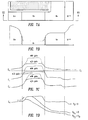
- Fig. 3A is a view of a portion of MOSFET 10 along cross-section III-III shown in Fig. 1
- Fig. 3B shows a profile of the dopant concentration along cross-section III-III at a drain voltage of zero.
- the depletion regions surrounding the source-to-body junction S/B and the drain-to-body junction D/B are shown in Fig. 3B .
- the corresponding energy bands are shown in Fig. 3C , which displays a conduction band E c , a valence band E v , and an intrinsic level E i , along with the Fermi level E f in equilibrium.
- the source-to-body junction creates a built-in energy barrier which prevents electrons from flowing from the source to the drain.
- Fig. 3D is a similar energy band diagram which shows only the conduction band E c .
- the energy barrier between the source and body is clearly evident.
- Fig. 3E shows the changes in the conduction band as the voltage at the drain is progressively raised to a level V D1 > 0 and then to a level V D2 > V D1 . Since the body region is not fully depleted, as shown in Fig. 3B , the application of a reverse bias between the drain and body does not lower the source-body barrier height.
- MOSFET 10 avoids a punchthrough condition (where the depletion regions around the source-body and drain-body junctions meet) by preventing its body region from becoming completely depleted and maintaining its built-in source-to-body energy barrier at all levels of the drain voltage. This property is characteristic of a long-channel MOSFET.
- Fig. 4 shows that a parasitic bipolar transistor also resides within MOSFET 10, having a base region represented by the undepleted body region of the MOSFET. Unless precautions are taken, this parasitic bipolar transistor can produce undesirable operating conditions.
- the source-to-body short is generally needed in conventional MOSFETs for several reasons.
- the body region must have a well-defined potential in order to prevent the threshold voltage of the MOSFET from drifting upward and downward uncontrollably.
- the threshold voltage of the device would tend to increase.
- the source-body short is needed to prevent snapback in the parasitic bipolar transistor, an undesirable phenomenon which leads to a substantial reduction of the off-state breakdown voltage of the device (referred to as BV cco breakdown in bipolar transistors).
- a major disadvantage of having an integral source-body short is that it must be included in every vertical MOSFET cell, thereby wasting valuable area and requiring a larger cell pitch.
- a larger cell pitch results in fewer cells and a lower total gate width per unit area, which in turn increases the on-resistance of the MOSFET.
- the minimum width of the source-body short region for a planar DMOSFET and a trenched-gate MOSFET, respectively is about 4 ⁇ m.
- ACCUFET 60 is a trenched-gate device which uses a semiconductor material of a single conductivity type but in different doping concentrations. Its gate is doped with P-type material such that the lightly-doped N- region 61 is fully depleted when the gate is turned off. Accordingly, the ACCUFET's leakage characteristic is that of a device which relies on an electrically induced potential barrier created by the gate rather than the built-in voltage of a PN junction.
- Fig. 7A shows a portion of ACCUFET 60 taken at cross-section VII-VII in Fig. 6 .
- Figs. 7B and 7C show the doping concentration profile and energy bands, respectively, at cross-section VII-VII.
- the influence of the gate in forming an energy barrier is evident from Fig. 7C , where the intrinsic level E i in the lightly doped region 61 is below the Fermi level (i.e., N-type) without the assistance of the gate but crosses the Fermi level (acting like an electrically-induced P-type region) when the gate is driven high.
- Fig. 7D shows that the energy barrier is almost immediately lowered by the application of any drain-to-source bias V D .
- the ACCUFET is further described in US patent No. 5,856,692 .
- PT-FET 80 includes a P-body region 81 which is of opposite conductivity type to its N+ source region 82 and N+ drain region 83.
- the gate 84 is doped with P-type material, and the "mesa" between the gate trenches is made narrow.
- the doping of P-body region 81 is so light that any small amount of drain voltage V D fully depletes the body region. This is evident from Figs. 9B and 9C , which show the doping profile at cross-section IX-IX in Fig.
- the PT-FET In its off-state, then, the PT-FET relies on the effect of the P-type gate on the P-type body material in the narrow mesa between the gate trenches to increase the height of the energy barrier between the source and body regions and thereby minimize its leakage current.
- the gate does not materially affect the depletion of the P-body region. Depletion spreading in the P-body region occurs almost entirely as a result of the PN junctions between the body region and the source and drain regions, respectively.
- DIBL drain-induced barrier lowering
- US 5,405,794 discloses a method for producing a vertical double diffused metal-on-semiconductor device, the method involving the formation of horizontally separated bodies of heavily doped Si and sources by a self-aligned process and a lift-off process along with the formation of trenches having negatively-sloped side-walls.
- the MOSFET of this invention is a vertical trenched-gate device according to claim 1 which includes source and drain regions of a first conductivity type and an intervening body region of a second conductivity type.
- the gate is formed in trenches, and the source and body regions are formed in "mesas" between the gate trenches.
- the doping concentration and profile and the vertical dimension of the body region are established such that, absent the effect of the gate, the body region does not become fully depleted at normal levels of source-drain voltage V DS and, in the preferred embodiment, at any voltage less than a V DS which causes junction avalanche breakdown to occur in the device.
- the gate is doped with material of the first conductivity type.
- the doping concentration and profile of the body and the horizontal dimension of the body region i.e., the width of the mesa
- the doping concentration and profile of the body and the horizontal dimension of the body region are established such that the body region does become depleted from the combined effects of the source-body and drain-body junctions and the gate when the gate is biased at the same potential as the source (the "source” for this purpose being defined as the more negative of the source/drain terminals in an N-channel MOSFET and the more positive of the source/drain terminals in a P-channel MOSFET).
- the MOSFET of this invention generally has a off-state leakage current which is lower than that of either an ACCUFET or an PT-FET, and it defaults to a normally "off” device in the absence of a defined gate potential. Without the influence of the gate, the MOSFET behaves like an "off" open base bipolar transistor. On the other hand, since the body region is depleted under the influence of the gate, the MOSFET of this invention requires no source-to-body short and therefore can be fabricated with a greater cell packing density than would otherwise be possible.
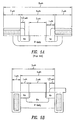
- MOSFET 100 is formed in a heavily-doped N++ substrate 101 which includes an N to N+ epitaxial (epi) layer 102.
- MOSFET 100 includes a gate 103 formed in a series of trenches 104 that extend downward from the top surface of the substrate 101 and are arrayed in a pattern of parallel stripes. The various arms of gate 103 are electrically connected together. Each arm of gate 103 is formed of polysilicon doped with N-type material and is separated from the semiconductor material of substrate 101 by an oxide layer 105.
- MOSFET 100 includes three active MOSFET cells 100A, 100B and 100C, along with a diode cell 100D which provides breakdown protection for active MOSFET cells 100A-100C and is described below.
- Each of active MOSFET cells 100A-100C includes an N+ source region 106 and a P-body region 107.
- the N+ source regions of the cells are electrically connected together in a conventional manner, as are the P-body regions of the cells.
- Epi layer 102 along with substrate 101 form a drain region 108.
- MOSFET 100 is a long-channel MOSFET, which means that the P-body regions have a length Y which is typically greater than their width X.
- N+ source regions 106 Electrical contact is made to N+ source regions 106 by means of a metal contact (not shown).
- the contact can be formed using a mask or, preferably, by using a self-aligned contact process wherein the gate is protected curing contact etching, not by photoresist, but by a thick overlying oxide or nitride layer.
- Fig. 11 illustrates a detailed view of active cell 100B, showing the depletion regions surrounding the PN junction between N+ source region 106 and P-body region 107 and the PN junction between drain region 108 and P-body region 107. As indicated, the length Y of P-body region 107 is established such that the depletion regions created by these two PN junctions alone do not occupy the whole of P-body region 107.
- the width X of the P-body region 107 (which is also the width of the "mesa" between the adjacent arms of gate 103 shown in Fig. 11 ) is sufficiently narrow that effect of the gate 103, which is formed of N-doped polysilicon, when added to the effect of the PN junctions, effectively depletes the entirety of P-body region 107.
- Diode cell 100D is described in US patent No. 5,856,692 .
- Diode cell 100D contains a P+ contact region 109 and a deep P+ region 110.
- a PN junction between deep P+ region 110 and epi layer 102 forms a diode D1 which is connected in parallel with the channels of active cells 100A-100C.
- Deep P+ region 110 (diode D2) can serve several functions. It can limit the strength of the electric field and resulting carrier formation near the corners of the trench 32 and thereby eliminate the need for a deep central diffusion in active cells 100A-100C. It can clamp the drain voltage so as to protect the oxide layer 105 from overstress due to excessive electric fields and to prevent junction avalanche breakdown from occurring in the active cells 100A-100C.
- the breakdown voltage of diode D1 is set by properly adjusting the doping concentration in deep P+ region 110.
- a diode cell is repeated at a specified periodicity throughout the cells of MOSFET 100 so that there is one diode cell for every N active cells.
- the breakdown voltage of the protective diode D 1 should be set slightly lower than the punchthrough voltage of the active cells 100A-100C by adjusting its anode concentration (i.e., the dopant concentration in deep P+ region 110).
- each of the two trenched gates surrounding a single mesa must each deplete 50% of the charge in the body region.
- the average concentration in the body region is N B ⁇ Q D X Dp
- a "stripe" cell geometry is used, and if the mesa width is greater than the trench width, a closed cell geometry is used.
- the energy barrier at the source-body junction has a low point near the center of the mesa, whereas with the MOSFET of this invention the energy barrier has a low point near the wall of the trench (i.e., the interface between the gate oxide and the silicon).
- the wall of the trench i.e., the interface between the gate oxide and the silicon.
- the principles of this invention can be combined with other features, such as the "1 of N" diode clamp taught in the above-referenced Application Serial No. 08/459,555.
- the MOSFET of this invention can also be used for bidirectional current blocking, where the source and drain are interchangeable, so long as the proper range of gate voltages is maintained by the controlling circuitry.
- the bidirectional diode clamp described in US 5,856,692 is also applicable to this invention.
Landscapes
- Insulated Gate Type Field-Effect Transistor (AREA)
- Metal-Oxide And Bipolar Metal-Oxide Semiconductor Integrated Circuits (AREA)
Description
- This invention relates to metal-oxide-silicon field-effect transistors (MOSFETs) and in particular to a type of power MOSFET in which the gate is formed in a trench.
- The primary performance objective for a power MOSFET switch is the achievement of the lowest possible on-resistance for a given breakdown voltage rating. The breakdown voltage is a measure of the ability of the MOSFET to withstand voltage when it is turned off, and the on-resistance is a measure of the ability of the MOSFET to carry a current with a minimal loss of power when it is turned on. The on-resistance is defined as the ratio of drain-to-source voltage to drain current when the switch is turned on.
- Structurally, power MOSFETs fall into two main categories. In lateral MOSFETs, the current flow is primarily "lateral" between source and drain regions that are formed at the surface of the substrate. In vertical MOSFETs, the current flow is primarily "vertical" between a source region located at the top surface of the substrate and a drain region located adjacent the backside of the substrate. In one subcategory of vertical MOSFETs, the gate is formed in a trench which extends into the top surface of the substrate. A trench-gated MOSFET is exemplified in the cross-sectional view of
Fig. 1 , which shows aMOSFET 10 having anN+ source region 11, a drain region 12 which includes anN++ substrate 13 and an N-epitaxial (epi)layer 14, and a P-body region 15. Current flows betweensource region 11 and drain region 12 through a channel in P-body region 15 adjacent the side wall of trenchedgate 16. Viewed from above, the trench appears as a pattern which divides the MOSFET into geometric cells. The cells may be rectangular, square, hexagonal or some other shape. A planar double-diffused MOSFET is exemplified byMOSFET 20 shown inFig. 2 , having anN+ source region 21, adrain region 22 which includes anN++ substrate 23 and an N-epi layer 24, and a P-body region 25. Current flows betweensource region 21 and drainregion 22 through a channel in P-body region 25 directly under agate 26. - In both of
MOSFETs metal layers body contact regions Body regions 15,25 are doped with P-type ions to the point that neither body region becomes completely depleted, even at high drain-to-source or gate-to-drain potentials. Because the body regions are not depleted and are always shorted to the source regions, the voltage applied toMOSFETs -
Fig. 3A is a view of a portion ofMOSFET 10 along cross-section III-III shown inFig. 1 , andFig. 3B shows a profile of the dopant concentration along cross-section III-III at a drain voltage of zero. The depletion regions surrounding the source-to-body junction S/B and the drain-to-body junction D/B are shown inFig. 3B . The corresponding energy bands are shown inFig. 3C , which displays a conduction band Ec, a valence band Ev, and an intrinsic level Ei, along with the Fermi level Ef in equilibrium. The source-to-body junction creates a built-in energy barrier which prevents electrons from flowing from the source to the drain.Fig. 3D is a similar energy band diagram which shows only the conduction band Ec. The energy barrier between the source and body is clearly evident. Finally,Fig. 3E shows the changes in the conduction band as the voltage at the drain is progressively raised to a level VD1 > 0 and then to a level VD2 > VD1. Since the body region is not fully depleted, as shown inFig. 3B , the application of a reverse bias between the drain and body does not lower the source-body barrier height. ThusMOSFET 10 avoids a punchthrough condition (where the depletion regions around the source-body and drain-body junctions meet) by preventing its body region from becoming completely depleted and maintaining its built-in source-to-body energy barrier at all levels of the drain voltage. This property is characteristic of a long-channel MOSFET. - As shown in the equivalent circuit diagram of
Fig. 4 , because the source and body regions ofMOSFET 10 are shorted together, the PN diode represented by the drain-to-body junction appears "anti-parallel", i.e., parallel to the normal path of current through MOSFET 10 (from the drain to the source) but opposite in direction. The disadvantage of having the source-body short inMOSFET 10 is a loss of bidirectional current blocking capability and in some applications unwanted PN diode conduction, which can lead to charge storage near the drain-body junction, large reverse recovery times, ringing, etc.Fig. 4 shows that a parasitic bipolar transistor also resides withinMOSFET 10, having a base region represented by the undepleted body region of the MOSFET. Unless precautions are taken, this parasitic bipolar transistor can produce undesirable operating conditions. - Despite these disadvantages, the source-to-body short is generally needed in conventional MOSFETs for several reasons. First and foremost, the body region must have a well-defined potential in order to prevent the threshold voltage of the MOSFET from drifting upward and downward uncontrollably. For example, if the source-body junction were to become reverse-biased, as a result of the well-known "body effect" the threshold voltage of the device would tend to increase. Second, the source-body short is needed to prevent snapback in the parasitic bipolar transistor, an undesirable phenomenon which leads to a substantial reduction of the off-state breakdown voltage of the device (referred to as BVcco breakdown in bipolar transistors). This problem is especially acute for MOSFETs having design breakdown voltages over 30 V, since the snapback voltage of the parasitic bipolar transistor may be only 10 or 20 V. Operating at 500 V and snapping back to 20 V, for example, would lead to destructive currents in the device.
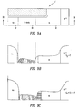
- A major disadvantage of having an integral source-body short is that it must be included in every vertical MOSFET cell, thereby wasting valuable area and requiring a larger cell pitch. A larger cell pitch results in fewer cells and a lower total gate width per unit area, which in turn increases the on-resistance of the MOSFET. For example, as shown in
Figs. 5A and 5B , the minimum width of the source-body short region for a planar DMOSFET and a trenched-gate MOSFET, respectively, is about 4 µm. In the planar DMOSFET, where the length of the gate is limited to at least around 4 µm, this implies a minimum cell pitch of 8 µm, and even in the trenched-gate MOSFET the source-body short limits the cell pitch to about 5 µm. - Two types of trenched-gate MOSFETs have been proposed to eliminate the need for a source-body short. One type, known as an accumulation mode FET or ACCUFET, is shown in cross-section in
Fig. 6 . ACCUFET 60 is a trenched-gate device which uses a semiconductor material of a single conductivity type but in different doping concentrations. Its gate is doped with P-type material such that the lightly-doped N-region 61 is fully depleted when the gate is turned off. Accordingly, the ACCUFET's leakage characteristic is that of a device which relies on an electrically induced potential barrier created by the gate rather than the built-in voltage of a PN junction. -
Fig. 7A shows a portion ofACCUFET 60 taken at cross-section VII-VII inFig. 6 .Figs. 7B and 7C show the doping concentration profile and energy bands, respectively, at cross-section VII-VII. The influence of the gate in forming an energy barrier is evident fromFig. 7C , where the intrinsic level Ei in the lightlydoped region 61 is below the Fermi level (i.e., N-type) without the assistance of the gate but crosses the Fermi level (acting like an electrically-induced P-type region) when the gate is driven high.Fig. 7D shows that the energy barrier is almost immediately lowered by the application of any drain-to-source bias VD. The ACCUFET is further described inUS patent No. 5,856,692 . - The second type of device, sometimes referred to as a punchthrough FET or PT-FET, is illustrated in cross-section in
Fig. 8 . PT-FET 80 includes a P-body region 81 which is of opposite conductivity type to itsN+ source region 82 andN+ drain region 83. Unlike a conventional MOSFET, however, thegate 84 is doped with P-type material, and the "mesa" between the gate trenches is made narrow. Moreover, the doping of P-body region 81 is so light that any small amount of drain voltage VD fully depletes the body region. This is evident fromFigs. 9B and 9C , which show the doping profile at cross-section IX-IX inFig. 8 when VD equals 0 V and 0.1-1.0 V, respectively. Note fromFig. 9B that only a small portion of thebody region 81 remains undepleted at VD = 0 V and, as shown inFig. 9C , the body region is fully depleted when VD = 0.1-1.0 V. Since the body region is fully depleted, it does not float, and no external body bias is required to define and stabilize the threshold voltage. There is no "quasi neutral" region in the P-body in which to apply an externally defined body bias. In this way the problem of threshold voltage drift is avoided. - In its off-state, then, the PT-FET relies on the effect of the P-type gate on the P-type body material in the narrow mesa between the gate trenches to increase the height of the energy barrier between the source and body regions and thereby minimize its leakage current. The gate does not materially affect the depletion of the P-body region. Depletion spreading in the P-body region occurs almost entirely as a result of the PN junctions between the body region and the source and drain regions, respectively.
- As shown in
Fig. 9D , however, the fact that the body region is fully depleted at small levels of VD means that, despite the P-type gate and narrow mesa, drain-induced barrier lowering (DIBL) occurs at small levels of VD. DIBL gives rise to a diffusion current which has a maximum limit determined by the charge carrier velocity. Thus in some situations the PT-FET may suffer from an unacceptably high leakage current. - The PT-FET is further described in
US patent No. 5,592,005 . -
US 5,405,794 discloses a method for producing a vertical double diffused metal-on-semiconductor device, the method involving the formation of horizontally separated bodies of heavily doped Si and sources by a self-aligned process and a lift-off process along with the formation of trenches having negatively-sloped side-walls. - The MOSFET of this invention is a vertical trenched-gate device according to
claim 1 which includes source and drain regions of a first conductivity type and an intervening body region of a second conductivity type. The gate is formed in trenches, and the source and body regions are formed in "mesas" between the gate trenches. - The doping concentration and profile and the vertical dimension of the body region (i.e., the distance between the source-body junction and the drain-body junction) are established such that, absent the effect of the gate, the body region does not become fully depleted at normal levels of source-drain voltage VDS and, in the preferred embodiment, at any voltage less than a VDS which causes junction avalanche breakdown to occur in the device.
- Furthermore, the gate is doped with material of the first conductivity type. The doping concentration and profile of the body and the horizontal dimension of the body region (i.e., the width of the mesa) are established such that the body region does become depleted from the combined effects of the source-body and drain-body junctions and the gate when the gate is biased at the same potential as the source (the "source" for this purpose being defined as the more negative of the source/drain terminals in an N-channel MOSFET and the more positive of the source/drain terminals in a P-channel MOSFET).
- The MOSFET of this invention generally has a off-state leakage current which is lower than that of either an ACCUFET or an PT-FET, and it defaults to a normally "off" device in the absence of a defined gate potential. Without the influence of the gate, the MOSFET behaves like an "off" open base bipolar transistor. On the other hand, since the body region is depleted under the influence of the gate, the MOSFET of this invention requires no source-to-body short and therefore can be fabricated with a greater cell packing density than would otherwise be possible.
-
-
Fig.. 1 illustrates a cross-sectional view of a conventional trenched-gate MOSFET. -
Fig. 2 illustrates a cross-sectional view of a conventional planar double-diffused vertical MOSFET. -
Fig. 3A illustrates a portion of the MOSFET ofFig. 1 taken at cross-section III-III. -
Fig. 3B illustrates a graph showing the dopant concentration profile of the MOSFET ofFig. 1 . -
Fig. 3C illustrates a graph showing the energy bands of the MOSFET ofFig. 1 . -
Fig. 3D illustrates a graph showing the conduction band of the MOSFET ofFig. 1 at zero drain voltage. -
Fig. 3E illustrates a graph showing the conduction band of the MOSFET ofFig. 1 at progressively increasing levels of drain voltage. -
Fig. 4 illustrates a schematic diagram of a conventional MOSFET having a source-body short. -
Figs. 5A and 5B illustrate cross-sectional views of a planar double-diffused and trenched-gate MOSFET, respectively, showing the area required for the source-body short. -
Fig. 6 illustrates a cross-sectional view of an accumulation mode MOSFET. -
Fig. 7A illustrates a portion of the MOSFET ofFig. 6 taken at cross-section VII-VII. -
Fig. 7B illustrates a graph showing the dopant concentration profile of the MOSFET ofFig. 6 . -
Fig. 7C illustrates a graph showing the energy bands of the MOSFET ofFig. 6 with and without gate drive. -
Fig. 7D illustrates a graph showing the conduction band of the MOSFET ofFig. 6 at progressively increasing levels of drain voltage. -
Fig. 8 illustrates a cross-sectional view of a punchthrough MOSFET. -
Fig. 9A illustrates a portion of the MOSFET ofFig. 8 taken at cross-section IX-IX. -
Fig. 9B illustrates a graph showing the dopant concentration profile and depletion regions of the MOSFET ofFig. 8 at a drain voltage of zero. -
Fig. 9C illustrates a graph showing the dopant concentration profile and depletion regions of the MOSFET ofFig. 8 at a small drain voltage. -
Fig. 9D illustrates a graph showing the conduction band of the MOSFET ofFig. 8 at progressively increasing levels of drain voltage. -
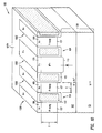
Fig. 10 illustrates a three-dimensional cross-sectional view of a long-channel MOSFET in accordance with this invention. -
Fig. 11 is a detailed cross-sectional view of a single cell of the MOSFET shown inFig. 10 . - A three-dimensional cross-sectional view of a
MOSFET 100 in accordance with this invention is shown inFig. 10 .MOSFET 100 is formed in a heavily-dopedN++ substrate 101 which includes an N to N+ epitaxial (epi)layer 102.MOSFET 100 includes agate 103 formed in a series oftrenches 104 that extend downward from the top surface of thesubstrate 101 and are arrayed in a pattern of parallel stripes. The various arms ofgate 103 are electrically connected together. Each arm ofgate 103 is formed of polysilicon doped with N-type material and is separated from the semiconductor material ofsubstrate 101 by anoxide layer 105.MOSFET 100 includes threeactive MOSFET cells active MOSFET cells 100A-100C and is described below. - Each of
active MOSFET cells 100A-100C includes anN+ source region 106 and a P-body region 107. The N+ source regions of the cells are electrically connected together in a conventional manner, as are the P-body regions of the cells.Epi layer 102 along withsubstrate 101 form adrain region 108.MOSFET 100 is a long-channel MOSFET, which means that the P-body regions have a length Y which is typically greater than their width X. - Electrical contact is made to
N+ source regions 106 by means of a metal contact (not shown). The contact can be formed using a mask or, preferably, by using a self-aligned contact process wherein the gate is protected curing contact etching, not by photoresist, but by a thick overlying oxide or nitride layer. -
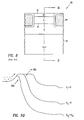
Fig. 11 illustrates a detailed view ofactive cell 100B, showing the depletion regions surrounding the PN junction betweenN+ source region 106 and P-body region 107 and the PN junction betweendrain region 108 and P-body region 107. As indicated, the length Y of P-body region 107 is established such that the depletion regions created by these two PN junctions alone do not occupy the whole of P-body region 107. - However, the width X of the P-body region 107 (which is also the width of the "mesa" between the adjacent arms of
gate 103 shown inFig. 11 ) is sufficiently narrow that effect of thegate 103, which is formed of N-doped polysilicon, when added to the effect of the PN junctions, effectively depletes the entirety of P-body region 107. - Diode cell 100D is described in
US patent No. 5,856,692 . Diode cell 100D contains aP+ contact region 109 and adeep P+ region 110. A PN junction betweendeep P+ region 110 andepi layer 102 forms a diode D1 which is connected in parallel with the channels ofactive cells 100A-100C. Deep P+ region 110 (diode D2) can serve several functions. It can limit the strength of the electric field and resulting carrier formation near the corners of the trench 32 and thereby eliminate the need for a deep central diffusion inactive cells 100A-100C. It can clamp the drain voltage so as to protect theoxide layer 105 from overstress due to excessive electric fields and to prevent junction avalanche breakdown from occurring in theactive cells 100A-100C. The breakdown voltage of diode D1 is set by properly adjusting the doping concentration indeep P+ region 110. Preferably, a diode cell is repeated at a specified periodicity throughout the cells ofMOSFET 100 so that there is one diode cell for every N active cells. - Punchthrough is avoided in
MOSFET 100 by satisfying certain minimum criteria for the body doping concentration. In a two-sided junction formed between thebody region 107 and thedrain region 108 ofMOSFET 100, the charge per unit area is given as:
- Assuming uniform doping in the two regions, the peak field at the junction is given by:

- With a voltage drop on each side of the junction


which sums to the total voltage
with Q'D = QD/A. Substituting xDn from equation (1) to eliminate the drain depletion region yields
meaning that the minimum body charge to avoid punchthrough can be found (approximately) by using the quadratic formula as a function of the desired voltage Vj and the base width (channel length). While a longer channel results in more body charge, it undesirably increases the on-resistance, thereby limiting xDp to the range of 0.5 to 1.5 µm in practical devices. Given a specific drain doping ND (e.g., between 1 x 10¹⁷ and 2 x 1019 cm-3) the breakdown voltage of the protective diode D1 should be set slightly lower than the punchthrough voltage of theactive cells 100A-100C by adjusting its anode concentration (i.e., the dopant concentration in deep P+ region 110). - To assure that the
body region 107 is fully depleted at a gate-to-source voltage of zero volts, each of the two trenched gates surrounding a single mesa must each deplete 50% of the charge in the body region. Given a total charge Q'D in the body region and a depth xDp, the average concentration in the body region is
- The lateral spreading and lateral charge depletion from only the gate are then


- The depletion region extending laterally (in the y direction) only from the gate becomes fully depleted when

- Preferably, if the mesa width is less than the trench width, a "stripe" cell geometry is used, and if the mesa width is greater than the trench width, a closed cell geometry is used.
- With the punchthrough FET described in
US 5,856,692 , the energy barrier at the source-body junction has a low point near the center of the mesa, whereas with the MOSFET of this invention the energy barrier has a low point near the wall of the trench (i.e., the interface between the gate oxide and the silicon). Thus current leakage in a punchthrough FET occurs first near the center of the mesa, whereas with the MOSFET of this invention current leakage occurs first near the wall of the trench. - The principles of this invention can be combined with other features, such as the "1 of N" diode clamp taught in the above-referenced Application Serial No. 08/459,555. The MOSFET of this invention can also be used for bidirectional current blocking, where the source and drain are interchangeable, so long as the proper range of gate voltages is maintained by the controlling circuitry. The bidirectional diode clamp described in
US 5,856,692 , is also applicable to this invention. - The foregoing embodiments are intended to be illustrative and not limiting. Numerous additional embodiments in accordance with the principles of this invention will be apparent to those skilled in the art. The broad scope of this invention is limited only by the following claims.
Claims (6)
- A trenched-gate power MOSFET (100) comprising:a semiconductor substrate (101,102);a gate (103) positioned in a trench (104), said trench (104) extending into said substrate (102) from a top surface thereof, said gate (103) being doped with material of a first conductivity type;a source region (106) of said first conductivity type adjacent said top surface;a body region (107) of a second conductivity type opposite to said first conductivity type underlying said source region (106) and forming a source-body junction with said source region (106);a drain region (108) of said first conductivity type underlying said body region (107) and forming a drain-body junction with said body region (107),wherein a doping concentration and profile of said body region (107) and a distance between said source-body junction and said drain-body junction are such that, at any source-drain voltage less than a source-drain voltage which causes junction avalanche breakdown to occur in said power MOSFET (100), a combined effect of said source-body junction and said drain-body junction is insufficient to cause said body region (107) to become depleted whereas a combined effect of said source-body junction, said drain-body junction and said gate (103) is sufficient to cause said body region (107) to be substantially depleted when said gate (103) is biased at a voltage equal to a voltage at said source region (106).
- The trenched-gate power MOSFET of claim 1 wherein a length of said body region (107) measured between said source-body junction and said drain-body junction is greater than a width of said body region (107) measured in a direction perpendicular to a direction of said length.
- The trenched-gate power MOSFET of claim 1 wherein said body region (107) is formed in a mesa, said mesa being formed between said trench (104) and a second trench (105), said second trench (105) being located on an opposite side of said mesa from said trench (104).
- The trenched-gate power MOSFET of claim 1 wherein said substrate (101,102) comprises an epitaxial layer (102), said trench (104) extending into said epitaxial layer (102).
- The trenched-gate power MOSFET of claim 1 comprising a plurality of said trenches (104,105), said trenches (104,105) being arrayed in a pattern of parallel stripes.
- The trenched-gate power MOSFET of claim 1 wherein said trench (104) comprises polysilicon.
Applications Claiming Priority (3)
| Application Number | Priority Date | Filing Date | Title |
|---|---|---|---|
| US651232 | 1996-05-22 | ||
| US08/651,232 US5998834A (en) | 1996-05-22 | 1996-05-22 | Long channel trench-gated power MOSFET having fully depleted body region |
| PCT/US1997/008187 WO1997044828A1 (en) | 1996-05-22 | 1997-05-21 | Long channel trench-gated power mosfet having fully depleted body region |
Publications (3)
| Publication Number | Publication Date |
|---|---|
| EP0902980A1 EP0902980A1 (en) | 1999-03-24 |
| EP0902980A4 EP0902980A4 (en) | 1999-06-16 |
| EP0902980B1 true EP0902980B1 (en) | 2008-10-22 |
Family
ID=24612075
Family Applications (1)
| Application Number | Title | Priority Date | Filing Date |
|---|---|---|---|
| EP97926508A Expired - Lifetime EP0902980B1 (en) | 1996-05-22 | 1997-05-21 | Long channel trench-gated power mosfet having fully depleted body region |
Country Status (7)
| Country | Link |
|---|---|
| US (1) | US5998834A (en) |
| EP (1) | EP0902980B1 (en) |
| JP (2) | JP4286321B2 (en) |
| KR (1) | KR100381845B1 (en) |
| AU (1) | AU3125797A (en) |
| DE (1) | DE69739058D1 (en) |
| WO (1) | WO1997044828A1 (en) |
Families Citing this family (26)
| Publication number | Priority date | Publication date | Assignee | Title |
|---|---|---|---|---|
| US5998834A (en) * | 1996-05-22 | 1999-12-07 | Siliconix Incorporated | Long channel trench-gated power MOSFET having fully depleted body region |
| DE69941769D1 (en) * | 1998-02-02 | 2010-01-21 | Cree Inc | Sic transistor |
| US6104068A (en) * | 1998-09-01 | 2000-08-15 | Micron Technology, Inc. | Structure and method for improved signal processing |
| US6320222B1 (en) * | 1998-09-01 | 2001-11-20 | Micron Technology, Inc. | Structure and method for reducing threshold voltage variations due to dopant fluctuations |
| GB9820904D0 (en) * | 1998-09-26 | 1998-11-18 | Koninkl Philips Electronics Nv | Bi-directional semiconductor switch and switch circuit for battery-powered equipment |
| JP3494063B2 (en) * | 1999-02-24 | 2004-02-03 | トヨタ自動車株式会社 | Semiconductor device |
| US6855983B1 (en) * | 1998-11-10 | 2005-02-15 | Toyota Jidosha Kabushiki Kaisha | Semiconductor device having reduced on resistance |
| US6777745B2 (en) * | 2001-06-14 | 2004-08-17 | General Semiconductor, Inc. | Symmetric trench MOSFET device and method of making same |
| US20060170053A1 (en) * | 2003-05-09 | 2006-08-03 | Yee-Chia Yeo | Accumulation mode multiple gate transistor |
| JP3744513B2 (en) * | 2003-05-30 | 2006-02-15 | トヨタ自動車株式会社 | diode |
| JP4445403B2 (en) | 2005-01-24 | 2010-04-07 | 株式会社東芝 | Manufacturing method of semiconductor device |
| KR100616159B1 (en) * | 2005-06-29 | 2006-08-28 | 주식회사 한국오도텍 | Vinyl pack fragrance and its manufacturing method |
| US9054183B2 (en) * | 2012-07-13 | 2015-06-09 | United Silicon Carbide, Inc. | Trenched and implanted accumulation mode metal-oxide-semiconductor field-effect transistor |
| US9696736B2 (en) | 2013-03-15 | 2017-07-04 | Fairchild Semiconductor Corporation | Two-terminal current limiter and apparatus thereof |
| US9679890B2 (en) | 2013-08-09 | 2017-06-13 | Fairchild Semiconductor Corporation | Junction-less insulated gate current limiter device |
| US9735147B2 (en) * | 2014-09-15 | 2017-08-15 | Fairchild Semiconductor Corporation | Fast and stable ultra low drop-out (LDO) voltage clamp device |
| JP6478316B2 (en) | 2014-11-10 | 2019-03-06 | ローム株式会社 | Semiconductor device having trench gate structure and manufacturing method thereof |
| DE102014119395B4 (en) * | 2014-12-22 | 2022-10-06 | Infineon Technologies Ag | Transistor device with field electrode |
| DE102018106670B4 (en) * | 2018-03-21 | 2025-02-06 | Infineon Technologies Ag | Silicon carbide semiconductor device with trench gate structure and a source region in an upper region of a mesa section |
| US10510836B1 (en) * | 2018-08-08 | 2019-12-17 | Infineon Technologies Austria Ag | Gate trench device with oxygen inserted si-layers |
| JP7224823B2 (en) * | 2018-09-19 | 2023-02-20 | キヤノン株式会社 | Photodetector |
| JP7063218B2 (en) * | 2018-09-27 | 2022-05-09 | 株式会社デンソー | Silicon carbide semiconductor device |
| US11728422B2 (en) * | 2019-11-14 | 2023-08-15 | Stmicroelectronics S.R.L. | Power MOSFET device having improved safe-operating area and on resistance, manufacturing process thereof and operating method thereof |
| CN113838936B (en) | 2020-06-23 | 2025-10-17 | 意法半导体股份有限公司 | 4H-SiC electronic device with improved short circuit performance and method of manufacturing the same |
| IT202000015076A1 (en) | 2020-06-23 | 2021-12-23 | St Microelectronics Srl | ELECTRONIC DEVICE IN 4H-SIC WITH IMPROVED SHORT-CIRCUIT PERFORMANCE, AND RELATED MANUFACTURING METHOD |
| US12495577B2 (en) | 2022-08-17 | 2025-12-09 | Analog Devices, Inc. | Self-aligned silicide gate for discrete shielded-gate trench power MOSFET |
Family Cites Families (8)
| Publication number | Priority date | Publication date | Assignee | Title |
|---|---|---|---|---|
| JP2859351B2 (en) * | 1990-02-07 | 1999-02-17 | 三菱電機株式会社 | Method for manufacturing semiconductor device |
| JP2837033B2 (en) * | 1992-07-21 | 1998-12-14 | 三菱電機株式会社 | Semiconductor device and manufacturing method thereof |
| JP2561413B2 (en) * | 1993-02-23 | 1996-12-11 | 日産自動車株式会社 | Semiconductor device |
| JPH07202182A (en) * | 1993-12-28 | 1995-08-04 | Nissan Motor Co Ltd | Semiconductor device |
| JP3481287B2 (en) * | 1994-02-24 | 2003-12-22 | 三菱電機株式会社 | Manufacturing method of semiconductor device |
| US5405794A (en) * | 1994-06-14 | 1995-04-11 | Philips Electronics North America Corporation | Method of producing VDMOS device of increased power density |
| US5592005A (en) * | 1995-03-31 | 1997-01-07 | Siliconix Incorporated | Punch-through field effect transistor |
| US5998834A (en) * | 1996-05-22 | 1999-12-07 | Siliconix Incorporated | Long channel trench-gated power MOSFET having fully depleted body region |
-
1996
- 1996-05-22 US US08/651,232 patent/US5998834A/en not_active Expired - Lifetime
-
1997
- 1997-05-21 JP JP54252197A patent/JP4286321B2/en not_active Expired - Fee Related
- 1997-05-21 KR KR10-1998-0709589A patent/KR100381845B1/en not_active Expired - Fee Related
- 1997-05-21 AU AU31257/97A patent/AU3125797A/en not_active Abandoned
- 1997-05-21 DE DE69739058T patent/DE69739058D1/en not_active Expired - Lifetime
- 1997-05-21 EP EP97926508A patent/EP0902980B1/en not_active Expired - Lifetime
- 1997-05-21 WO PCT/US1997/008187 patent/WO1997044828A1/en not_active Ceased
-
2008
- 2008-11-12 JP JP2008289444A patent/JP4981013B2/en not_active Expired - Fee Related
Also Published As
| Publication number | Publication date |
|---|---|
| EP0902980A1 (en) | 1999-03-24 |
| US5998834A (en) | 1999-12-07 |
| DE69739058D1 (en) | 2008-12-04 |
| JP2009060136A (en) | 2009-03-19 |
| WO1997044828A1 (en) | 1997-11-27 |
| KR100381845B1 (en) | 2003-07-16 |
| EP0902980A4 (en) | 1999-06-16 |
| AU3125797A (en) | 1997-12-09 |
| KR20000016027A (en) | 2000-03-25 |
| JP4286321B2 (en) | 2009-06-24 |
| JP2000511353A (en) | 2000-08-29 |
| JP4981013B2 (en) | 2012-07-18 |
Similar Documents
| Publication | Publication Date | Title |
|---|---|---|
| EP0902980B1 (en) | Long channel trench-gated power mosfet having fully depleted body region | |
| US10157983B2 (en) | Vertical power MOS-gated device with high dopant concentration N-well below P-well and with floating P-islands | |
| US6285060B1 (en) | Barrier accumulation-mode MOSFET | |
| US6444527B1 (en) | Method of operation of punch-through field effect transistor | |
| KR100628938B1 (en) | Power Semiconductor Devices with Improved High Frequency Switching and Breakdown Characteristics | |
| US7479678B2 (en) | Semiconductor element and method of manufacturing the same | |
| WO2005076362A2 (en) | Semiconductor device containing dielectrically isolated doped field shield region | |
| US10490658B2 (en) | Power semiconductor device | |
| JP7697777B2 (en) | Trench-gate silicon carbide devices | |
| US11367775B1 (en) | Shielding structure for SiC devices | |
| US12119377B2 (en) | SiC devices with shielding structure | |
| US20210399128A1 (en) | Power devices with a hybrid gate structure | |
| WO2005053033A2 (en) | Trench insulated gate field-effect transistor | |
| US12176423B2 (en) | FinFET power semiconductor devices | |
| EP1178539A2 (en) | Schottky field-effect transistor | |
| EP4258361A2 (en) | Vertical shielded gate accumulation field effect transistor | |
| CN120826008A (en) | Silicon carbide devices with trench gates |
Legal Events
| Date | Code | Title | Description |
|---|---|---|---|
| PUAI | Public reference made under article 153(3) epc to a published international application that has entered the european phase |
Free format text: ORIGINAL CODE: 0009012 |
|
| 17P | Request for examination filed |
Effective date: 19981127 |
|
| AK | Designated contracting states |
Kind code of ref document: A1 Designated state(s): DE IT NL |
|
| A4 | Supplementary search report drawn up and despatched |
Effective date: 19990506 |
|
| AK | Designated contracting states |
Kind code of ref document: A4 Designated state(s): DE IT NL |
|
| RIC1 | Information provided on ipc code assigned before grant |
Free format text: 6H 01L 29/10 A, 6H 01L 29/76 B, 6H 01L 29/94 B, 6H 01L 31/062 B, 6H 01L 31/113 B, 6H 01L 31/119 B |
|
| 17Q | First examination report despatched |
Effective date: 20040128 |
|
| GRAP | Despatch of communication of intention to grant a patent |
Free format text: ORIGINAL CODE: EPIDOSNIGR1 |
|
| GRAS | Grant fee paid |
Free format text: ORIGINAL CODE: EPIDOSNIGR3 |
|
| GRAA | (expected) grant |
Free format text: ORIGINAL CODE: 0009210 |
|
| AK | Designated contracting states |
Kind code of ref document: B1 Designated state(s): DE IT NL |
|
| REF | Corresponds to: |
Ref document number: 69739058 Country of ref document: DE Date of ref document: 20081204 Kind code of ref document: P |
|
| PLBE | No opposition filed within time limit |
Free format text: ORIGINAL CODE: 0009261 |
|
| STAA | Information on the status of an ep patent application or granted ep patent |
Free format text: STATUS: NO OPPOSITION FILED WITHIN TIME LIMIT |
|
| 26N | No opposition filed |
Effective date: 20090723 |
|
| PGFP | Annual fee paid to national office [announced via postgrant information from national office to epo] |
Ref country code: DE Payment date: 20140529 Year of fee payment: 18 Ref country code: NL Payment date: 20140526 Year of fee payment: 18 Ref country code: IT Payment date: 20140526 Year of fee payment: 18 |
|
| REG | Reference to a national code |
Ref country code: DE Ref legal event code: R119 Ref document number: 69739058 Country of ref document: DE |
|
| PG25 | Lapsed in a contracting state [announced via postgrant information from national office to epo] |
Ref country code: IT Free format text: LAPSE BECAUSE OF NON-PAYMENT OF DUE FEES Effective date: 20150521 |
|
| REG | Reference to a national code |
Ref country code: NL Ref legal event code: MM Effective date: 20150601 |
|
| PG25 | Lapsed in a contracting state [announced via postgrant information from national office to epo] |
Ref country code: NL Free format text: LAPSE BECAUSE OF NON-PAYMENT OF DUE FEES Effective date: 20150601 Ref country code: DE Free format text: LAPSE BECAUSE OF NON-PAYMENT OF DUE FEES Effective date: 20151201 |