EP1174899A2 - Electron source device - Google Patents
Electron source device Download PDFInfo
- Publication number
- EP1174899A2 EP1174899A2 EP01306009A EP01306009A EP1174899A2 EP 1174899 A2 EP1174899 A2 EP 1174899A2 EP 01306009 A EP01306009 A EP 01306009A EP 01306009 A EP01306009 A EP 01306009A EP 1174899 A2 EP1174899 A2 EP 1174899A2
- Authority
- EP
- European Patent Office
- Prior art keywords
- emitter
- nitride
- carbide
- electrode
- silicon
- Prior art date
- Legal status (The legal status is an assumption and is not a legal conclusion. Google has not performed a legal analysis and makes no representation as to the accuracy of the status listed.)
- Withdrawn
Links
Images



Classifications
-
- H—ELECTRICITY
- H01—ELECTRIC ELEMENTS
- H01J—ELECTRIC DISCHARGE TUBES OR DISCHARGE LAMPS
- H01J3/00—Details of electron-optical or ion-optical arrangements common to two or more basic types of discharge tubes or lamps
- H01J3/02—Electron guns
- H01J3/021—Electron guns using a field emission, photo emission, or secondary emission electron source
- H01J3/022—Electron guns using a field emission, photo emission, or secondary emission electron source with microengineered cathode, e.g. Spindt-type
Definitions
- the present invention relates generally to production of an electron beam using an electron source device. More specifically, the present invention relates to new structures and new materials for a self-aligned electron source device that produces a beam of electrons from a composite emitter that is co-axially surrounded by a cavity that includes extractor and focus electrodes separated by dielectric layers.
- Spindt type emitters are one type of emitter used in a field emission display (FED).
- FED field emission display
- An analogous technology to the FED is the cathode ray tube (CRT) used as a display in television sets and computer monitors.
- CRT cathode ray tube
- the FED is one type of device that incorporates an electron field emitter.
- an emitter electrode has a plurality of Spindt emitters formed thereon.
- a Spindt emitter is a conical cathode connected to the emitter electrode at its base and having a sharp tip (needlelike point) at its vertex.
- a extractor electrode having a circular aperture therein is positioned proximate to the tip and is electrically biased relative to the emitter electrode so that electron emission is induced from the tip. Basically, when a sufficient voltage differential is applied between the extractor electrode and the tip of the Spindt emitter, electrons quantum mechanically tunnel out of the tip. The emitted electrons are accelerated towards a positively biased anode spaced approximately 100 ⁇ m to 200 ⁇ m away from the tip of the Spindt emitter. It is commonplace to use a glass substrate coated with a conductive material such as indium tin oxide (ITO) for the anode of the FED.
- ITO indium tin oxide
- the voltage potentials between the emitter electrode and the extractor electrode can be on the order of 10 V to 150 V, and the voltage potentials between the emitter electrode and the anode can be on the order of a few hundred volts to several kilovolts or more.
- a variety of methods are known in the art that are suitable for making the electron field emitters described above. By way of example, a general discussion of one method is disclosed in "Physical Properties of Thin-Film Field Emission Cathodes with Molybdenum Cones," by Spindt et al, published in the Journal of Applied Physics, Vol. 47, No. 12, December 1976.
- each image pixel in the display is serviced by an array, usually a very large group, of individual field emitters connected to a common emitter electrode.
- Each pixel includes a phosphor coating that is operative to emit visible light in response to the electron beams incident on that pixel.
- the electron beam from a single emitter will diverge (spread out) in the direction of the pixel.
- the area of the pixel is larger than the width of the electron beam from a single emitter. Accordingly, an array of emitters is required to produce light of sufficient intensity from the pixel.
- the array of emitters provides for emitter redundancy in case one or more of the field emitters is inoperative.
- Electrostatically focusing an electron beam is a technique that is well understood in the art.
- a negatively biased focus electrode can be used to electrostatically deflect the electron beam towards an axis of the beam. Resulting is an electron beam that converges into a narrower beam.
- Another example of electrostatic focusing is the use of a dielectric layer that co-axially encircles the path taken by the electron beam. The natural divergence of the beam allows the beam to impinge on the dielectric layer thereby inducing a negative electrostatic charge in the dielectric layer. Eventually, the induced charge reaches the potential of the emitter electrode. Consequently, the electrostatic charge causes the width of the beam to contract inward towards the axis of the beam.
- another method for focusing the beam includes the use of focusing ridges that are positioned on opposing sides of an array of emitters.
- the ridges are biased to a potential that is close to or equal the voltage of the emitters.
- the ridges electrostatically influence the trajectories of the electron beams from the array so that the phosphor in the target pixel is substantially struck by all of the emitted electrons.
- a general discussion of collimating electron beams in FED's can be found in the following issued U.S. Patents: 5,070,282; 5,235,244; and 5,528,103.
- the above mentioned focusing techniques are intended to sufficiently narrow the beam so that it strikes the target pixel with a beam width that is adequate to produce light of a desired intensity.
- the beam is narrowed by those focusing techniques, the beam is still too wide for use in high density storage applications. Furthermore, misalignment between the focusing element and the beam axis of the emitter will result in some deflection of the beam, but that deflection will not defeat proper operation of the FED. On the other hand, in a high density storage device it is desirable to have a very narrow and precisely aligned electron beam that can be accurately directed towards the storage media.
- FED's can be used in portable display applications, it is desirable to reduce power consumption by using low work function materials to reduce the bias voltages between electrodes.
- low work function materials is that the microelectronic fabrication processes used in making the display can cause variations in the work function of the emitter material.
- the work function increases from its known value to a higher value. Consequently, the work function can vary from emitter to emitter, resulting in variations in electron beam current among the emitters of the FED.
- an electron source device that is adapted to emit a single, narrowly focused, electron beam, that includes an emitter structure having a uniform cone shape and a very sharp tip, that has an emitter made from a combination of materials having a work function that does not change during the course of microelectronic fabrication of the device, and that has an emitter that is self-aligned with the electrodes of the device.
- the present invention is an improvement in the design of electron source devices. Particularly, the present invention includes improvements in the materials and structure used for an emitter of an electron source device.
- the aforementioned disadvantages associated with focusing the electron bean are addressed by providing a cavity that is self-aligned with a vertex of the emitter so that the electrodes of the device are co-axially aligned with the beam axis of the emitter.
- the problems associated with an unstable work function for the emitter are addressed by using new combinations of materials that yield a stable work function.
- a uniform cone shape and a sharp tip for the emitter are addressed by using a composite of materials to form the emitter.
- the present invention is embodied in a self-aligned electron source device for generating a beam of electrons.
- the device includes a first dielectric layer upon which an emitter electrode is formed.
- a second dielectric layer is formed on the emitter electrode followed by forming an extractor electrode on the second dielectric layer.
- a third dielectric layer is formed on the extractor electrode followed by forming a focus electrode on the third dielectric layer.
- a cavity is formed by a single photolithography step followed by a single etch step. The cavity extends through the focus electrode, the third dielectric layer, the extractor electrode, and the second dielectric layer. The cavity terminates at the emitter electrode.
- a composite emitter is formed on the emitter electrode.
- the composite emitter includes a base that is formed on the emitter electrode and a substantially conical tip that is formed on the base.
- the tip terminates at a vertex to form a sharp point.
- the cavity is disposed symmetrically about the composite emitter and is co-axially aligned with the vertex of the tip so that the cavity is centered about a beam axis through the vertex of the tip and the cavity and the composite emitter are substantially self-aligned relative to each other, resulting in an electrostatic lens assembly (including the extractor and focus electrodes) that is symmetric with respect to the beam axis of the composite emitter.
- electrons disposed proximate to the vertex of the tip can be extracted by the extractor electrode and focused into a smaller beam of electrons by the focus electrode.
- the electron beam can be used to write data to and to read data from advanced data storage systems including ultra-high density storage devices.
- the tip of the composite emitter can be made from a variety of electrically conductive materials including a refractory metal, a metal alloy, a silicon alloy, an electroformable metal, a carbide, or a nitride.
- the first dielectric layer is formed on a substrate.
- any one of the electrodes can be made from an electrically conductive composite material comprising a fine-grained amorphous layer formed on top of an adhesion layer.
- the emitter electrode is made from a heavily doped semiconductor material.
- the base of the composite emitter is made from titanium, chromium, or doped silicon.
- any one of the second and third dielectric layers comprises an etch stop dielectric layer and a pull-back dielectric layer formed on top of the etch stop dielectric.
- the pull back dielectric layer includes a pull-back surface profile that is operative to reduce charge accumulation on cavity-facing portions of the dielectric layers.
- the tip is made from an electroformable metal so that the vertex of the tip forms an atomically sharp point.
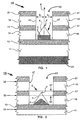
- FIG. 1 is a cross-sectional view of the self-aligned electron emission device according to the present invention.
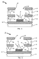
- FIG. 2 is a cross-sectional view illustrating the position of the vertex relative to an upper surface and a lower surface of the extractor electrode according to the present invention.
- FIG. 3 is a cross-sectional view illustrating an atomically sharp vertex of an electroformed tip according to the present invention.
- FIG. 4 is a cross-sectional view of the device illustrating the cavity having a negative slope in the direction of the focus electrode according to the present invention.
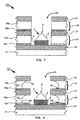
- FIG. 5 and FIG. 6 are cross-sectional views illustrating a dielectric layer having a pull-back surface profile according to the present invention.
- FIG. 7 is a cross-sectional view illustrating second and third dielectric layers having an etch stop dielectric layer and a pull-back dielectric layer according to the present invention.
- FIG. 8 is a cross-sectional view illustrating a pull-back surface profile etched into the dielectric layer of FIG. 7.
- FIG. 9 is a cross-sectional view illustrating electrodes made from an electrically conductive composite material according to the present invention.
- FIG. 10 is a cross-sectional view illustrating the relationship between the height of the composite emitter to the diameter of the cavity at the focus electrode and the height of the second dielectric layer according to the present invention.
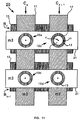
- FIG. 11 is a top plan view of an array of self-aligned electron emission devices electrically configured to be enabled individually or in groups according to the present invention.
- FIG. 12 is a table illustrating metal alloys and silicon alloys for the tip according to the present invention.
- the present invention is embodied in a self-aligned electron source device that includes a first dielectric layer having an emitter electrode formed thereon, a second dielectric layer formed on the emitter electrode, an extractor electrode formed on the second dielectric layer, a third dielectric layer formed on the extractor electrode, and a focus electrode formed on the third dielectric layer.
- a cavity extending through the focus electrode, the third dielectric layer, the extractor electrode, and the second dielectric layer is formed in the device and terminates at the emitter electrode.
- a composite emitter is formed in the cavity and comprises a base formed on the emitter electrode and a substantially conical tip formed on the base and terminating at a vertex.
- the cavity is centered about the composite emitter and is co-axially aligned with a beam axis through the vertex so that the composite emitter and the cavity are substantially self-aligned with each other.
- the extractor electrode and the focus electrode form an electrostatic lens assembly that is adapted to extract electrons from the tip of the composite emitter and to focus the electrons into a narrow beam along the beam axis of the composite emitter.
- the cavity is formed by a single photolithography step and a single dry etching step, thereby eliminating multiple patterning and etching steps that can increase manufacturing complexity, cost, and can introduce defects or contamination that reduce manufacturing yield. Furthermore, subsequent deposition of the materials for the base and tip of the composite emitter results in self-alignment between the cavity and the emitter.
- the composite emitter particularly the tip, can be made from materials selected to produce a stable work function that does not change during fabrication of the device. Additionally, the base and the tip are made from different materials that can be selected to yield a smooth conical tip having a sharp point at its vertex.
- a self-aligned electron source device 10 includes a first dielectric layer 11. An electrically conductive emitter electrode 13 is formed on the first dielectric layer 11. A second dielectric layer 15 is formed on the emitter electrode 13 . An extractor electrode 17 is formed on the second dielectric layer 15. A third dielectric layer 19 is formed on the extractor electrode 17 . A focus electrode 21 is formed on the third dielectric layer 19. A cavity 23 is formed by etching thorough all of the above electrodes and dielectric layers except the emitter electrode 13 so that the cavity 23 terminates at the emitter electrode 13 . After forming the cavity 23, a composite emitter 1 is formed in the cavity 23.
- the composite emitter 1 includes a base 3 that is formed on the emitter electrode 13 and a substantially conical tip 5 that is formed on the base 3.
- the tip 5 terminates at a vertex V.
- the tip 5 has a sharp point at the vertex V.
- a sharp point at the vertex V increases the field strength at the vertex V thereby enhancing electron emission from the tip 5.
- the cavity 23 symmetrically surrounds the composite emitter 1 (i.e. the cavity 23 is centered about the composite emitter 1 ) as shown by arrows S 1 and S 2 and is co-axially aligned with a beam axis B (shown as a dashed arrow) through the vertex V so that the cavity 23 and the composite emitter 1 are substantially self-aligned with each other.
- the cavity 23 can have substantially vertical sidewall surfaces 47 so that the cavity 23 has a substantially cylindrical shape.
- the self-aligned electron source device 10 can be installed in an enclosure (not shown) having a partial vacuum therein so that the cavity 23 is under a partial vacuum.
- the cavity 23 is under a partial vacuum of at least 10 -5 torr or less.
- One advantage of the self-aligned relationship between the cavity 23 and the composite emitter 1 is that electrons (not shown) extracted from the vertex V by the extractor electrode 17 are focused by the focus electrode 21 into a focused beam of electrons (not shown) substantially along the beam axis B.
- the focus electrode 21 narrows the cross-sectional width of the electron beam.
- Those electrons can impinge on a predetermined target location on a storage media (not shown) positioned opposite the focus electrode.
- the electron beam can be used to store and access information on the storage media. The distance between the vertex V of the tip 5 and the storage media and the width of the electron beam at the target location will be application specific.
- the cavity 23 can be formed by a single photolithography step and a single dry etching step.
- a conventional reactive ion etching (RIE) process in the semiconductor industry can be used to form the cavity 23.
- RIE reactive ion etching
- the first dielectric layer 11 can be formed on a substrate 25 .
- the substrate 25 can be a semiconductor substrate.
- the substrate 25 can be silicon.
- One advantage to using a semiconductor for the substrate 25 is that active circuits for addressing the composite emitter 1 can be formed in the substrate 25.
- Other suitable materials for the substrate 25 include glass and quartz.
- the vertex V of the tip 5 is positioned intermediate between an upper surface 31 and a lower surface 33 (both shown in dashed line) of the extractor electrode 17.
- the vertex V can be positioned above the upper surface 31 or below the lower surface 33, in a preferred embodiment, the most efficacious extraction of electrons from the tip 5 results from positioning the vertex V intermediate between the upper surface 31 and the lower surface 33 of the extractor electrode 17.
- the base 3 of the composite emitter 1 need not have a substantially cylindrical shape as shown in FIG. 1.
- the base 3 can have an arcuate shape or a cone shape as illustrated in FIG. 2.
- the actual shape of the base 3 will depend on the material selected for the base 3 and the deposition process used to form the base 3.
- the device 10 can be used to fabricate the device 10. For instance, conventional photolithography and etching techniques can be used to form the cavity 23.
- the cavity 23, can be etched using RIE, for example.
- the dielectric layers and the electrodes can be formed using conventional thin-film deposition techniques.
- the composite emitter 1 can be formed by using evaporation techniques to deposit the base 3 and the tip 5 .
- Materials for the base 3 of the composite emitter 1 include titanium ( Ti ), chromium (Cr), niobium (Nb), and resistive materials such as doped silicon (Si).
- the tip 5 of the composite emitter 1 can be made from a refractory metal.
- the refractory metal for the tip 5 includes but is not limited to those shown in Table 1 below.
- the tip 5 of the composite emitter 1 can be made from a metal alloy or a silicon alloy.
- the alloys for the tip 5 include but are not limited to the alloys listed in Table 2 below.
- FIG. 12 illustrates a matrix of alloys for the tip 5 and includes the metal and silicon alloys of Table 2.
- a suitable alloy for the tip 5 is indicated by a check at an intersection of a row with a column. Column numbers increase from left to right as shown by arrow C and row numbers increase from top to bottom as shown by arrow R in FIG. 12.
- silicon (Si) in row 10 can be combined with zirconium (Zr) in column 5 to form a silicon zirconium (SiZr) alloy for the tip 5.
- tungsten (W) in row 7 can be combined with chromium (Cr) in column 8 to form a tungsten chromium (WCr) alloy.
- WCr tungsten chromium
- the metal alloys for the tip 5 include the refractory metals listed in Table 1 above. Accordingly, a metal alloy can be made from any two different materials (excluding silicon ( Si ) ) listed in FIG. 12. Furthermore, a silicon alloy can be made from any two different materials listed in FIG. 12.
- One method for forming the tip 5 from the alloys of FIG. 12 is to use a coevaporation process.
- a silicon (Si) source and a titanium source (Ti) can be evaporated at the same time to form the tip 5 .
- a source comprising both silicon (Si) and titanium (Ti) can be evaporated to form the tip 5 .
- the tip 5 of the composite emitter 1 is made from an electroformable metal.
- the process for low temperature electroforming of the tip 5 is well known in the art.
- the tip 5 can be electroformed by first depositing the material for the tip 5 on the base 3.
- the device 10 is heated to a temperature of about half the melting point of the metal used for the tip 5.
- An extraction field is applied to the extraction electrode 17 at a field strength below that necessary to extract electrons from the tip 5.
- the material used for the tip 5 begins to flow under the force of the extraction field. Resulting is an atomically sharp point at the vertex V of the tip 5.
- Suitable materials for the electroformable metal include but are not limited to those listed in Table 3 below.
- the tip 5 of the composite emitter 1 can be made from a carbide (C).
- the carbide (C) for the tip 5 includes but is not limited to the electrically conductive carbides shown in Table 4 below.
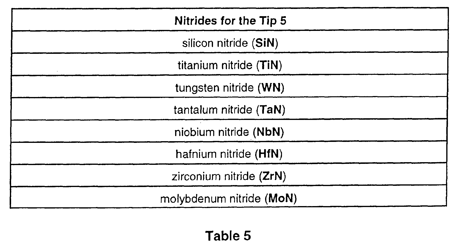
- the tip 5 of the composite emitter 1 can be made from a nitride ( N ).
- the nitride ( N ) for the tip 5 includes but is not limited to the electrically conductive nitrides shown in Table 5 below.
- the first dielectric layer 11 , the second dielectric layer 15, and the third dielectric layer 19 can be made from a dielectric material that includes but is not limited to silicon oxide, silicon nitride, silicon carbide, silicon oxide on top of silicon carbide, and silicon oxide on top of silicon nitride.
- the emitter electrode 13, the extractor electrode 17, and the focus electrode 21 can be made from an electrically conductive material that includes but is not limited to aluminum (Al), tungsten (W), gold (Au), platinum (Pt), copper (Cu), chromium (Cr), titanium (Ti), tantalum (Ta), tantalum aluminum (TaAI), titanium nitride ( TiN ), tungsten nitride (WN), tantalum nitride (TaN), tantalum tungsten nitride (TaWN), titanium carbide (TiC), aluminum carbide (AIC), tantalum carbide (TaC), and tungsten carbide (WC).
- the emitter electrode 13 is made from an electrically conductive material comprising a heavily doped semiconductor.
- the heavily doped semiconductor can be silicon (Si).
- At least a portion of the cavity 23 has a negative slope 41 in a direction towards the focus electrode 21 (i.e. the cavity narrows in the direction of the focus electrode 21).
- the negative slope 41 is operative to reduce charge accumulation on surfaces of the second 15 and third 19 dielectric layers that face the cavity 23.
- the second dielectric layer 15 and/or the third dielectric layer 19 includes a cavity facing portion 43 and 45 respectively, having a pull-back surface profile 40 that is operative to reduce charge accumulation on the cavity facing portions 43 and 45 respectively by positioning those portions away from the bore of the cavity 23.
- the emitter electrode 13 and the extractor electrode 17 serve as etch stops for the second dielectric layer 15 and/or the third dielectric layer 19 as shown by arrows 49.
- the pull-back surface profile 40 can be an arcuate shape as illustrated in FIG. 5 or the pull-back surface profile 40 can be a sloped shape (not shown).
- the cavity 23 can have the substantially vertical sidewall surfaces 47 as illustrated in FIG. 5 or the cavity 23 can have the negative slope 41 as illustrated in FIG. 6 and discussed above in reference to FIG. 4.
- the cavity 23 can also have a positive slope (not shown) in a direction toward the focus electrode 21.
- Other shapes for the pull-back surface profile 40 are possible and the shape of the pull-back surface profile 40 will depend on the etching process used.
- the second and third dielectric layers 15 and 19 respectively can include a dielectric and mechanical strength enhancement layer 15a and 19a of silicon nitride ( SiN ) or silicon carbide (SiC) and a pull-back dielectric layer 15b and 19b of silicon oxide ( SiO 2 ) formed on top of the dielectric and mechanical strength enhancement layers 15a and 19a.
- a dielectric and mechanical strength enhancement layer 15a and 19a of silicon nitride ( SiN ) or silicon carbide (SiC) and a pull-back dielectric layer 15b and 19b of silicon oxide ( SiO 2 ) formed on top of the dielectric and mechanical strength enhancement layers 15a and 19a.
- the dielectric and mechanical strength enhancement layers 15a and 19a enhance the resistance to dielectric breakdown in high voltage operation of the device 10 . Additionally, the dielectric and mechanical strength enhancement layers 15a and 19a mechanically strengthen the adjacent metal layers that form the emitter electrode 13 and the extractor electrode 17.
- the pull-back dielectric layers 15b and 19b can include the pull-back surface profile 40, as illustrated in FIG. 8.
- the thickness of the pull-back dielectric layers 15b and 19b can be from about 100 nanometers to about 2000 nanometers.
- the etch stop dielectric layers 15a and 19a can have a thickness from about 50 nanometers to about 200 nanometers.
- the pull-back surface profile 40 can be an arcuate shape as illustrated in FIG. 8 or the pull-back surface profile 40 can be a sloped shape.
- the arcuate shape or the sloped shape can have a positive or a negative slope in the direction of the focus electrode 21.
- Other shapes for the pull-back surface profile 40 are possible and the shape of the pull-back surface profile 40 will depend on the etching process used.
- the emitter electrode 13, the extractor electrode 17, and the focus electrode 21 can be made from an electrically conductive composite material including a fine-grained amorphous layer 13b, 17b, and 21b respectively, formed on top of an adhesion layer 13a, 17a, and 21a respectively.
- the fine-grained amorphous layers 13b, 17b, and 21b can be a metal with a small grain structure, i.e. an amorphous structure like that of a metallic glass.
- the base 3 can be deposited onto the fine-grained or amorphous layer 13b with no preferred crystal orientation. Resulting is a smooth surface upon which the tip 5 can be grown.
- the smooth surface of the base 3 allows the tip 5 to grow with a smooth, uniform, and symmetrical cone shape that terminates at a sharp point at the vertex V.
- Materials for the fine-grained amorphous layer 13b , 17b, and 21b include but are not limited to titanium nitride ( TiN ), tantalum nitride (TaN), and tungsten nitride (WN) on top of any one of the following materials for the adhesion layer 13a, 17a, and 21a : titanium (Ti); aluminum ( Al ); tantalum (Ta); tungsten (W); and chromium (Cr).
- TiN titanium nitride
- TaN tantalum nitride
- WN tungsten nitride
- an electrode abutting surface 22 of any one of the first dielectric layer 11, the second dielectric layer 15 and the third dielectric layer 19 can be planarized to form a substantially flat surface.
- a planarization process such as chemical mechanical polishing (CMP) can be used to planarize the dielectric layers. Planarization results in a smooth and flat surface upon which to deposit the electrodes.
- CMP chemical mechanical polishing
- the emitter electrode 13, the extractor electrode 17, and the focus electrode 21 have a thickness of about 50 nanometers to about 200 nanometers.
- the second dielectric layer 15 has a thickness that is substantially equal to a height H of the composite emitter 1 at the vertex V of the tip 5.
- the cavity 23 has a diameter W at the focus electrode 21 that is substantially equal to the height H of the composite emitter 1 at the vertex V of the tip 5.
- the thickness of the second dielectric layer 15 and the diameter W of the cavity 23 will be determined by application specific parameters for the device 10 and can be controlled through the photolithography, deposition and etching steps used to fabricate the device 10.
- FIG. 11 illustrates a top plan view of an array 20.
- the device 10 is replicated four times (10a, 10b, 10c, and 10d) in the array 20 .
- FIG. 11 is not to be construed as limiting the number of devices 10 that can be arrayed as shown.
- the array 20 can include but is not limited to a 10 * 10 array of devices 10 .
- the array 20 includes two emitter electrodes 13 arranged into rows R n and R n+1 and two extractor electrodes 17 arranged into two columns C n and C n+1 . Although only two rows and two columns are illustrated, the array 20 can include any combination of rows and columns.
- the emitter electrode 13 in row R n can be connected to a low voltage relative to the extractor electrode 17 in column C n+1 to create an extraction field that will induce electrons to quantum tunnel off of the vertex V of the tip 5.
- the emitter electrode 13 in row R n can be connected to a GND terminal (not shown) of a power source and the extractor electrode 17 in column C n+1 can be connected to a positive terminal (not shown) of a power source.
- the focus electrode can be connected to the GND terminal or some other negative voltage source.
- the composite emitter 1 and a portion of the emitter electrode 13 are visible through the cavity 23 in the focus electrode 21. The symmetry between the composite emitter 1 and the cavity 23 is also illustrated in FIG. 11.
- FIG. 11 illustrates the relationship between the various metal layers used to implement the electrodes 13, 17, and 21.
- the emitter electrode 13 can be implemented in a metal one layer m1
- the extractor electrode 17 can be implemented in a metal two layer m2
- the focus electrode 21 can be implemented in a metal three layer m3.
- the number of metal layers will be determined by the semiconductor process used to fabricate the device 10 and the layout design rules for that process.
- the devices 10a, 10b, 10c, and 10d can have their respective electrodes individually connected to (i.e. in electrical communication with) active switching elements (not shown) such as a field-effect transistor (FET) that allow the devices in the array 20 to be switched “On” (emit electrons) or "Off” (no electron emission) by using digital logic gates to control the gate nodes of their respective FET's.
- active switching elements such as a field-effect transistor (FET) that allow the devices in the array 20 to be switched “On” (emit electrons) or “Off” (no electron emission) by using digital logic gates to control the gate nodes of their respective FET's.
- FET field-effect transistor
- MOSFET metal-oxide-semiconductor field-effect transistor
- the device 10b can have its emitter electrode 13 formed directly on a drain node of a FET.
- a gate node of the FET can be connected to a digital signal source adapted to turn the FET "On” or “Off”.
- a source node of the FET can be connected to a GND node of a power supply.
- An appropriate digital signal on the gate node of the FET can be used to turn the device 10b "On” or “Off”.
- the emitter electrode 13 is substantially at GND. Electron emission from the emitter 1 of the device 10b can be initiated by biasing the extractor electrode 17 to a positive potential relative to the emitter electrode 13 so that electrons quantum mechanically tunnel out of the tip 5 of the emitter 1.
- the drain node of the FET can be connected to the emitter electrode using a tungsten ( W ) plug, for example.
- the electrode 13 can be formed directly on a source node of a FET and the drain node of the FET can be connected to a GND node of a power supply.
Landscapes
- Cold Cathode And The Manufacture (AREA)
- Cathode-Ray Tubes And Fluorescent Screens For Display (AREA)
- Electrodes For Cathode-Ray Tubes (AREA)
Abstract
Description


Claims (17)
- An electron source device 10 comprising:a first dielectric layer 11;an emiter electrode 13 formed on the first dielectric layer 11;a composite emitter 1 including a base 3 formed on the emitter electrode 13 and a substantially conical tip 5 formed on the base 3 and terminating at a vertex V;a second dielectric layer 15 formed on the emitter electrode 13;an extracter electrode 17 formed on the second dielectric layer 15;a third dielectric layer 19 formed on the extractor electrode 17; anda focus electrode 21 formed on the third dielectric layer 19;the focus and extractor electrodes (21, 17) and the second and third dielectric layers (15, 19) include a cavity 23 extending from the focus electrode 21 and terminating at the emitter electrode 13, the cavity 23 symmetrically surrounds the composite emitter 1 and is co-axially aligned with the vertex V of the tip 5 so that the cavity 23 and the composite emitter 1 are substantially self-aligned relative to each other.
- The device of Claim 1, wherein the tip 5 of the composite emitter 1 is made from a refractory metal and the refractory metal includes a material selected from the group consisting of molybdenum, niobium, hafnium, zirconium, tantalum, tungsten, and vanadium.
- The device of Claim 1, wherein the tip 5 of the composite emitter 1 is made from a metal alloy and the metal alloy includes a combination of any two dissimilar materials selected from the group consisting of titanium, molybdenum, niobium, hafnium, zirconium, vanadium, tungsten, chromium, and tantalum.
- The device of Claim 1, wherein the tip 5 of the composite emitter 1 is made from an electroformable metal and the vertex V forms an atomically sharp point and the electroformable metal includes a material selected from the group consisting of tin, tin alloy, indium, indium alloy, magnesium, and magnesium alloy.
- The device of Claim 1, wherein the tip 5 of the composite emitter 1 is made from an electrically conductive carbide and the electrically conductive carbide includes a material selected from the group consisting of silicon carbide, titanium carbide, tungsten carbide, tantalum carbide, niobium carbide, hafnium carbide, zirconium carbide, and molybdenum carbide.
- The device of Claim 1, wherein the tip 5 of the composite emitter 1 is made from an electrically conductive nitride and the electrically conductive nitride includes a material selected from the group consisting of silicon nitride, titanium nitride, tungsten nitride, tantalum nitride, hafnium nitride, niobium nitride, zirconium nitride, and molybdenum nitride.
- The device of Claim 1, wherein the base 3 of the composite emitter 1 is a material selected from the group consisting of titanium, chromium, niobium, and doped silicon.
- The device of Claim 1, wherein any one of the dielectric layers (11, 15, 19) is made from a dielectric material selected from the group consisting of silicon oxide, silicon nitride, silicon carbide, silicon oxide on top of silicon carbide, and silicon oxide on top of silicon nitride.
- The device of Claim 1, wherein any one of the electrodes (13, 17, 21) is made from an electrically conductive material selected from the group consisting of aluminum, tungsten, gold, platinum, copper, chromium, titanium, tantalum, tantalum aluminum, titanium nitride, tungsten nitride, tantalum nitride, tantalum, tungsten nitride, titanium carbide, tantalum carbide, tungsten carbide, and aluminum carbide.
- The device of Claim 1, wherein any one of the electrodes (13, 17, 21) is made from an electrically conductive composite material comprising a fine-grained amorphous layer (13b, 17b, 21b) formed on top of an adhesion layer (13a, 17a, 21a),the fine-grained amorphous layer (13b, 17b, 21b) is a material selected from the group consisting of titanium nitride, tantalum nitride, and tungsten nitride, andthe adhesion layer (13a, 17a, 21a) is a material selected from the group consisting of titanium, aluminum, tantalum, tungsten, and chromium.
- The device of Claim 1, wherein the emitter electrode 13 is made from an electrically conductive material comprising a heavily doped semiconductor.
- The device of Claim 1, wherein any one of the second and third dielectric layers (15, 19) comprises a cavity-facing portion (43, 45) having a pull-back surface profile 40 that is operative to reduce electrical charge accumulation on the cavity-facing portion (43, 45) and the pull-back surface profile 40 includes a shape selected from the group consisting of a sloped shape and an arcuate shape.
- The device of Claim 12, wherein any one of the second and third dielectric layers (15, 19) comprises a dielectric and mechanical strength enhancement layer (15a, 19a) and a pull-back dielectric layer (15b, 19b) of silicon oxide formed on top of the dielectric and mechanical strength enhancement layer (15a, 19a),the pull-back dielectric layer (15b, 19b) includes the pull-back surface profile 40, andthe dielectric and mechanical strength enhancement layer (15a, 19a) is made from a material selected from the group consisting of silicon nitride and silicon carbide.
- The device of Claim 1, wherein at least a portion of the cavity 23 has a negative slope 41 in a direction towards the focus electrode 21.
- The device of Claim 1, wherein the tip 5 of the composite emitter 1 is made from a silicon alloy.
- The device of Claim 15, wherein the silicon alloy is a combination of silicon and a material selected from the group consisting of titanium, molybdenum, niobium, hafnium, zirconium, vanadium, tungsten, chromium, and tantalum.
- The device of Claim 1, wherein the emitter electrode 13 is formed directly on a node of a field-effect transistor selected from the group consisting of a drain node and a source node.
Applications Claiming Priority (2)
| Application Number | Priority Date | Filing Date | Title |
|---|---|---|---|
| US61787600A | 2000-07-17 | 2000-07-17 | |
| US617876 | 2000-07-17 |
Publications (2)
| Publication Number | Publication Date |
|---|---|
| EP1174899A2 true EP1174899A2 (en) | 2002-01-23 |
| EP1174899A3 EP1174899A3 (en) | 2002-09-18 |
Family
ID=24475402
Family Applications (1)
| Application Number | Title | Priority Date | Filing Date |
|---|---|---|---|
| EP01306009A Withdrawn EP1174899A3 (en) | 2000-07-17 | 2001-07-12 | Electron source device |
Country Status (4)
| Country | Link |
|---|---|
| EP (1) | EP1174899A3 (en) |
| JP (1) | JP2002083555A (en) |
| CN (1) | CN1334582A (en) |
| HK (1) | HK1043433A1 (en) |
Cited By (2)
| Publication number | Priority date | Publication date | Assignee | Title |
|---|---|---|---|---|
| FR2836279A1 (en) * | 2002-02-19 | 2003-08-22 | Commissariat Energie Atomique | Cathode structure of triode type, comprises electrode supporting layer of electron emitting material exposed through opening cut in grid electrode |
| WO2004079734A1 (en) * | 2003-01-14 | 2004-09-16 | Nm Spintronics Ab | System for electronic data storage |
Families Citing this family (8)
| Publication number | Priority date | Publication date | Assignee | Title |
|---|---|---|---|---|
| US6670628B2 (en) * | 2002-04-04 | 2003-12-30 | Hewlett-Packard Company, L.P. | Low heat loss and small contact area composite electrode for a phase change media memory device |
| KR20060011668A (en) * | 2004-07-30 | 2006-02-03 | 삼성에스디아이 주식회사 | Electron emitting device and method for manufacturing same |
| KR20060019846A (en) * | 2004-08-30 | 2006-03-06 | 삼성에스디아이 주식회사 | Electron-emitting device |
| KR20060095318A (en) * | 2005-02-28 | 2006-08-31 | 삼성에스디아이 주식회사 | Electron emitting device and method for manufacturing same |
| JP5723730B2 (en) * | 2011-09-05 | 2015-05-27 | 株式会社日立ハイテクノロジーズ | Emitter, gas field ion source, and ion beam device |
| CN104934275B (en) * | 2015-05-18 | 2018-01-09 | 北京大学 | Field Electron Emission cathode array based on metal molybdenum substrate and preparation method thereof |
| CN106691457B (en) * | 2016-12-30 | 2022-08-02 | 胡振强 | Fingerprint developing device |
| CN117174549A (en) * | 2022-05-26 | 2023-12-05 | 华为技术有限公司 | An electron source chip and its preparation method and electronic equipment |
Family Cites Families (9)
| Publication number | Priority date | Publication date | Assignee | Title |
|---|---|---|---|---|
| JP2719239B2 (en) * | 1991-02-08 | 1998-02-25 | 工業技術院長 | Field emission device |
| DE4325708C1 (en) * | 1993-07-30 | 1994-06-16 | Siemens Ag | Prodn. of electrically conducting point made of doped silicon@ - by forming mask with opening on substrate and producing doped silicon@ paint on exposed surface of substrate |
| US5564959A (en) * | 1993-09-08 | 1996-10-15 | Silicon Video Corporation | Use of charged-particle tracks in fabricating gated electron-emitting devices |
| FR2719156B1 (en) * | 1994-04-25 | 1996-05-24 | Commissariat Energie Atomique | Source of microtip electrons, microtips having two parts. |
| US5702281A (en) * | 1995-04-20 | 1997-12-30 | Industrial Technology Research Institute | Fabrication of two-part emitter for gated field emission device |
| AU5727496A (en) * | 1995-05-08 | 1996-11-29 | Advanced Vision Technologies, Inc. | Field emission display cell structure and fabrication proces s |
| KR100201553B1 (en) * | 1995-09-25 | 1999-06-15 | 하제준 | Field emitter array with integrated mosfet and manufacturing method thereof |
| US5869169A (en) * | 1996-09-27 | 1999-02-09 | Fed Corporation | Multilayer emitter element and display comprising same |
| US6465941B1 (en) * | 1998-12-07 | 2002-10-15 | Sony Corporation | Cold cathode field emission device and display |
-
2001
- 2001-07-10 JP JP2001208963A patent/JP2002083555A/en active Pending
- 2001-07-12 EP EP01306009A patent/EP1174899A3/en not_active Withdrawn
- 2001-07-17 CN CN01123054A patent/CN1334582A/en active Pending
-
2002
- 2002-07-11 HK HK02105161.0A patent/HK1043433A1/en unknown
Cited By (4)
| Publication number | Priority date | Publication date | Assignee | Title |
|---|---|---|---|---|
| FR2836279A1 (en) * | 2002-02-19 | 2003-08-22 | Commissariat Energie Atomique | Cathode structure of triode type, comprises electrode supporting layer of electron emitting material exposed through opening cut in grid electrode |
| WO2003071571A1 (en) * | 2002-02-19 | 2003-08-28 | Commissariat A L'energie Atomique | Cathode structure for an emission display |
| US7759851B2 (en) | 2002-02-19 | 2010-07-20 | Commissariat A L'energie Atomique | Cathode structure for emissive screen |
| WO2004079734A1 (en) * | 2003-01-14 | 2004-09-16 | Nm Spintronics Ab | System for electronic data storage |
Also Published As
| Publication number | Publication date |
|---|---|
| EP1174899A3 (en) | 2002-09-18 |
| CN1334582A (en) | 2002-02-06 |
| HK1043433A1 (en) | 2002-09-13 |
| JP2002083555A (en) | 2002-03-22 |
Similar Documents
| Publication | Publication Date | Title |
|---|---|---|
| US4904895A (en) | Electron emission device | |
| KR0181327B1 (en) | Field emission cathode with resistive gate areas and electron using the same | |
| EP1174899A2 (en) | Electron source device | |
| US5378182A (en) | Self-aligned process for gated field emitters | |
| US5734223A (en) | Field emission cold cathode having micro electrodes of different electron emission characteristics | |
| JPH09219144A (en) | Electric field emitting cathode and its manufacture | |
| JPH08236012A (en) | Field emission type cold cathode with focusing electrode | |
| US6822380B2 (en) | Field-enhanced MIS/MIM electron emitters | |
| US5719466A (en) | Field emission display provided with repair capability of defects | |
| US5587628A (en) | Field emitter with a tapered gate for flat panel display | |
| US5969467A (en) | Field emission cathode and cleaning method therefor | |
| US20060261724A1 (en) | Display using a movable electron field emitter and method of manufacture thereof | |
| JP2809078B2 (en) | Field emission cold cathode and method of manufacturing the same | |
| US6806488B2 (en) | Tunneling emitters and method of making | |
| JP2910837B2 (en) | Field emission type electron gun | |
| JPH0748346B2 (en) | Field emission cold cathode device | |
| Nagao et al. | Fabrication of a field emitter array with a built-in einzel lens | |
| US6902458B2 (en) | Silicon-based dielectric tunneling emitter | |
| Ngoc Minh et al. | Microelectron field emitter array with focus lenses for multielectron beam lithography based on silicon on insulator wafer | |
| US6852554B2 (en) | Emission layer formed by rapid thermal formation process | |
| JPH09270229A (en) | Field emission electron source | |
| JP3156903B2 (en) | Field emission type electron source | |
| US6960876B2 (en) | Electron emission devices | |
| US6787792B2 (en) | Emitter with filled zeolite emission layer | |
| US5874808A (en) | Low turn-on voltage volcano-shaped field emitter and integration into an addressable array |
Legal Events
| Date | Code | Title | Description |
|---|---|---|---|
| PUAI | Public reference made under article 153(3) epc to a published international application that has entered the european phase |
Free format text: ORIGINAL CODE: 0009012 |
|
| AK | Designated contracting states |
Kind code of ref document: A2 Designated state(s): AT BE CH CY DE DK ES FI FR GB GR IE IT LI LU MC NL PT SE TR |
|
| AX | Request for extension of the european patent |
Free format text: AL;LT;LV;MK;RO;SI |
|
| PUAL | Search report despatched |
Free format text: ORIGINAL CODE: 0009013 |
|
| AK | Designated contracting states |
Kind code of ref document: A3 Designated state(s): AT BE CH CY DE DK ES FI FR GB GR IE IT LI LU MC NL PT SE TR |
|
| AX | Request for extension of the european patent |
Free format text: AL;LT;LV;MK;RO;SI |
|
| 17P | Request for examination filed |
Effective date: 20030318 |
|
| AKX | Designation fees paid |
Designated state(s): DE FR GB |
|
| 17Q | First examination report despatched |
Effective date: 20040517 |
|
| STAA | Information on the status of an ep patent application or granted ep patent |
Free format text: STATUS: THE APPLICATION HAS BEEN WITHDRAWN |
|
| 18W | Application withdrawn |
Effective date: 20060109 |