EP1174721A2 - Jitter detecting apparatus and phase locked loop using the detected jitter - Google Patents
Jitter detecting apparatus and phase locked loop using the detected jitter Download PDFInfo
- Publication number
- EP1174721A2 EP1174721A2 EP01303813A EP01303813A EP1174721A2 EP 1174721 A2 EP1174721 A2 EP 1174721A2 EP 01303813 A EP01303813 A EP 01303813A EP 01303813 A EP01303813 A EP 01303813A EP 1174721 A2 EP1174721 A2 EP 1174721A2
- Authority
- EP
- European Patent Office
- Prior art keywords
- signal
- edge
- jitter
- signals
- value
- Prior art date
- Legal status (The legal status is an assumption and is not a legal conclusion. Google has not performed a legal analysis and makes no representation as to the accuracy of the status listed.)
- Granted
Links
Images



Classifications
-
- H—ELECTRICITY
- H03—ELECTRONIC CIRCUITRY
- H03L—AUTOMATIC CONTROL, STARTING, SYNCHRONISATION OR STABILISATION OF GENERATORS OF ELECTRONIC OSCILLATIONS OR PULSES
- H03L7/00—Automatic control of frequency or phase; Synchronisation
- H03L7/06—Automatic control of frequency or phase; Synchronisation using a reference signal applied to a frequency- or phase-locked loop
- H03L7/08—Details of the phase-locked loop
-
- G—PHYSICS
- G01—MEASURING; TESTING
- G01R—MEASURING ELECTRIC VARIABLES; MEASURING MAGNETIC VARIABLES
- G01R25/00—Arrangements for measuring phase angle between a voltage and a current or between voltages or currents
Definitions
- the present invention relates to jitter detecting, and more particularly, to a method and an apparatus for detecting a jitter amount using an analog-digital conversion circuit.
- the analog signal is binarized through a comparator, and a phase locked loop is applied to the binarized signal to make a system clock.
- Data is processed using the binarized signal and the system clock.
- a synchronism of the analog signal does not correspond accurately with that of the system clock, and a little phase difference exists, which is called a jitter.
- a method for binarizing, using the converted digital signal after converting the analog signal into the digital signal through the analog-digital converting process is used instead of binarizing the analog signal by directly using a comparator. Since the method for detecting a jitter used in the latter case detects a jitter value using a signal of one sampling point around the edge of the analog signal, the jitter value is not detected correctly if the analog signal is small or an error signal enters.
- Figure 1 is a block diagram of a general digital system including a jitter detecting circuit, wherein the system includes an A/D converter 100, a DC offset eliminator 110, a jitter detector 120, and a digital phase locked loop (PLL) circuit 130.
- the A/D converter 100 converts an analog input signal into a digital signal, and generates digital data corresponding to the digital signal.
- the DC offset eliminator 110 eliminates a direct current voltage offset from the digital data.
- the jitter detector 120 detects a jitter value from the offset-eliminated signal.
- the digital PLL circuit 130 generates a locked signal from the offset-eliminated signal, and the locked signal is generated as the system clock.
- Korean Patent P1998-0049210 published on 17 November 1998, applied for by the same inventor discloses a method for calculating a jitter value from analog/digital converted digital data.
- the analog to digital converted value itself, is small, and the jitter amount detected from the value is also small.
- an input signal having an error in which the amplitude of the signal greatly varies, there can be an error in the operation of the circuit itself.
- a jitter detector for detecting a jitter amount from signals derived from two sampling points around the edge of an analog/digital converted signal.
- a jitter value detecting circuit for detecting a jitter value of a signal which is converted into a digital signal from an analog signal input, wherein the jitter value detecting circuit comprising: an edge detector for discriminating signs of two signals derived from two continuous sampling points from the digitally converted input signal, and outputting the two signals as first and second edge signals, respectively, if the signs are different from each other; a comparator for outputting a signal having a smaller absolute value among the first and second edge signals output from the edge detector: an operating unit for dividing the absolute value output from the comparator by the sum of the absolute value of the first edge signal and that of the second edge signal, respectively: and an accumulator for accumulating outputs of the operating unit during a predetermined period, to obtain a jitter value of the predetermined period.
- the edge detector comprises: a delayer for delaying the digitally input signal by one system clock; and an edge generator for comparing signs of an output signal of the delayer with sign of the digitally input signal, and outputting the two signals as the first edge signal and the second edge signal, respectively, if the signs are different with each other.
- the edge generator comprises: a first bit detector for detecting a most significant bit of the input signal; a second bit detector for detecting a most significant bit of the input signal passing through the delayer; an exclusive OR calculator for performing an exclusive-OR (XOR) operation on the detected values of the first bit detector and the second bit detector; a first edge signal generator using output value of the exclusive OR calculator as a clock signal, and using the digital input signal as an input signal; and a second edge signal generator using the output value of the exclusive OR calculator as a clock signal simultaneously with the first edge signal generator, and using the digital input signal through the delayer as an input signal.
- XOR exclusive-OR
- a digital phase locked loop circuit comprising: a jitter signal generator having an edge detector for generating first and second edge signals by discriminating sign change from the continuous sampling points from a digital converted input signal; a comparator for outputting a signal having a smaller absolute value among the first and second edge signals output from the edge detector; an operating unit for dividing an absolute value output from the comparator by the sum of the absolute value of the first edge signal and that of the second edge signal to obtain a jitter signal as a result, and a phase locked signal generator for generating a phase locked signal, using a jitter signal generated from the jitter signal generator as a phase error signal.
- FIG. 2 is a block diagram of a jitter detecting circuit of an embodiment of the present invention, wherein the jitter detecting circuit includes an edge detector 200, a comparator 210, an operating unit 220, and an accumulator 230.
- the edge detector 200 discriminates whether the sign at two consecutive sampling points is changed from a digitally converted, DC offset removed input signal. If the sign is changed, a signal of the sampling point before the sign change and a signal after the sign change are output as the first and second edge signals respectively.
- the comparator 210 compares the first and second edge signals output from the edge detector 200, and outputs the signal having a smaller absolute value among the two signals.
- the operating unit 220 generates a jitter value which divides the smaller absolute value signal output from the comparator by the sum of the absolute values of the first edge signal and that of the second edge signals. This calculation uses a proportional formula of a triangle which will be described in detail hereinafter.
- the accumulator 230 accumulates the values output from the operating unit 220 during a predetermined period, and outputs the result as a jitter value of the predetermined period.
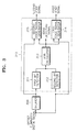
- FIG 3 is a detailed block diagram of the edge detector 200 of Figure 2 including a delayer 300 and an edge generator 310.
- the delayer 300 delays an (analog) input signal converted into digital by one clock signal of the corresponding system clock.
- the edge generator 310 compares a sign of the original digital converted input signal with a sign of the digital converted input signal delayed by one clock from the delayer 300, and if the signs are different from each other, the two signals are both considered edge signals. Then, the original digital converted signal and the delayed signal through the delayer 300 are output as the first and second edge signals respectively.
- the edge generator 310 includes a first bit detector 311 for detecting a most significant bit (MSD) of a digital converted input signal; a second bit detector 312 for detecting a most significant bit from the one clock delayed digital converted input signal through the delayer 300; an exclusive OR (XOR) calculator 313 for generating 0 when the extracted values of the first bit detector 311 and the second bit detector 312 are the same, and generating 1 when the extracted values are different; a first edge signal generator 314 using an output value of the exclusive OR calculator 313 as a clock, and using a digital input signal as an input signal, and a second edge signal generator 315 using the output value of the exclusive OR calculator 313 as a clock equally with the first edge signal generator 314, and using a delayed digital input signal from the delayer 310 as an input signal.
- MSD most significant bit
- XOR exclusive OR
- Figure 4 includes: first and second absolute value extractors 400, 410 for detecting respective absolute values of the first and second edge signals extracted in Figure 3; a minimum value extractor 420 for detecting a smaller value among the first and second absolute values; an adder 430 for adding the first and second absolute values; a divider 440 for dividing a smaller absolute value generated from the minimum value extractor 420 by an output value generated from the adder 430; and a counter and an accumulator 450 for accumulating jitter values calculated in the divider 440 whenever edges are generated, and generating the result as a jitter value of a predetermined period at every time interval.
- the counter and accumulator 450 can be set up in advance to generate a jitter value accumulated with desired gain for desired time interval received from a MICOM (not shown).
- a system clock is made from a PLL (Phase Locked Loop) circuit with an analog input signal, and then, data is processed using the system clock.
- PLL Phase Locked Loop
- the locked signal from the PLL circuit is synchronous with the analog input signal, the signal processing can be performed without a problem.
- the locked signal from the PLL circuit is not synchronous with the input signal because noise is mixed or another undesirable thing happens in the input signal, it is a problem for processing a signal. In the latter case, the time difference between the system clock and a zero level of the input signal is called a jitter.
- Figure 5a is an example of a signal without a jitter
- Figure 5b is an example of a signal with a jitter.
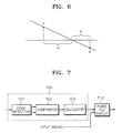
- Figure 6 magnifies and illustrates a part of signal around the edge in a signal with the jitter shown in Figure 5b.
- "a” and “b” in Figure 6 are amplitude of a sampling signal which can be obtained by sampling an analog input signal.
- "a"' and “b'” in Figure 6 are amounts of phase delay at time coordinates, that is, a jitter, and one of the two having a smaller absolute value is chosen as a jitter value, so that in Figure 6, b' is a jitter value.
- a sampling cycle is equal to a system clock cycle, so that b' added to a' equals a system clock.
- a jitter value calculation using the formula 1, is not affected by an amplitude of an input signal, so that an accurate jitter value can be obtained.
- This is implemented on the operating uit 220 of Figure 2, that is, the remaining composition except a counter and accumulator 450 of Figure 4.
- Figure 7 illustrates a phase locked loop using a jitter value as a phase error signal, wherein the phase locked loop includes a jitter signal generator 700 and a PLL circuit 710.
- the jitter signal generator 700 includes an edge detector 701, a comparator 702, and an operating unit 703.
- the edge detector 701 discriminates signs of two continuous signals from digital converted input signals, and if the signs are different from each other, the two signals are generated as first and second edge signals.
- the comparator 702 generates a signal having a smaller absolute value among the generated first and second edge values.
- the operating unit 703 divides the smaller absolute value of the edge signal generated from the PLL circuit 710 by the sum of the absolute values of the first signal and that of the second edge signal to obtain a jitter value.
- a calculation principle of the operating unit 703 is as described above with reference to Figure 6.
- the PLL circuit 710 uses a jitter signal generated from the jitter signal generator 701 as a phase error signal to obtain a phase locked signal.
- a jitter value can be suppressed to the maximum by a method for optimizing a focus loop or tracking loop in a servo part of an optical disc using the present invention described above.
- a jitter amount is detected with signals derived from two sampling points around the edge from the analog-digital converted signal, so that an accurate jitter amount can be detected regardless of the input signal amplitude, and an accurate and fast phase locked signal can be obtained using the jitter value.
Landscapes
- Physics & Mathematics (AREA)
- General Physics & Mathematics (AREA)
- Stabilization Of Oscillater, Synchronisation, Frequency Synthesizers (AREA)
- Synchronisation In Digital Transmission Systems (AREA)
- Signal Processing For Digital Recording And Reproducing (AREA)
- Dc Digital Transmission (AREA)
Abstract
Description
Claims (4)
- A jitter detecting circuit for detecting a jitter value of a signal which is converted into a digital signal from an analog signal input, wherein the jitter value detecting circuit comprises:an edge detector (200) for discriminating signs of two signals derived from continuous sampling points from the digitally converted input signal, and outputting the two signals as first and second edge signals, respectively, if the signs are different from each other;a comparator (210) for outputting a signal having a smaller absolute value among the first and second edge signals output from the edge detector;an operating unit (220) for dividing the absolute value output from the comparator by the sum of the absolute value of the first edge signal and that of the second edge signal; andan accumulator (230) for accumulating outputs of the operating unit during a predetermined period, to obtain a jitter value of the predetermined period.
- The jitter detecting circuit of claim 1, wherein the edge detector (200) comprises:a delayer (300) for delaying the digitally converted input signal by one system clock; andan edge generator (310) for comparing signs of an output signal of the delayer with signs of the digitally converted input signal, and outputting the two signals as the first edge signal and the second edge signal, respectively if the signs are different with each other.
- The jitter detecting circuit of claim 2, wherein the edge generator (310) comprises:a first bit detector (311) for detecting a most significant bit of the input signal;a second bit detector (312) for detecting a most significant bit of the input signal passing through the delayer;an exclusive OR calculator (313) for performing an exclusive-OR operation on the extracted values of the first bit detector and the second bit detector;a first edge signal generator (314) using output value of the exclusive OR calculator as a clock signal, and using the digital input signal as an input signal; anda second edge signal generator (315) using the output value of the exclusive OR calculator as a clock signal simultaneously with the first edge signal generator, and using the digital input signal through the delayer as an input signal.
- A digital phase locked loop comprises:
a jitter signal generator (700) having:an edge detector (701) for generating first and second edge signals by discriminating sign change from continuous sampling points from a digital converted input signal;a comparator (702) for outputting a signal having a smaller absolute value among the first and second edge signals output from the edge detector;an operating unit (703) for dividing an absolute value output from the comparator by the sum of the absolute value of the first edge signal and that of the second edge signal to obtain a jitter signal as a result; anda phase locked signal generator (710) for generating a phase locked signal, using the jitter signal generated from the jitter signal generator as a phase error signal.
Applications Claiming Priority (2)
| Application Number | Priority Date | Filing Date | Title |
|---|---|---|---|
| KR1020000041743A KR100694039B1 (en) | 2000-07-20 | 2000-07-20 | Jitter Detection Device and Phase-Locked Loop Using the Same |
| KR2000041743 | 2000-07-20 |
Publications (3)
| Publication Number | Publication Date |
|---|---|
| EP1174721A2 true EP1174721A2 (en) | 2002-01-23 |
| EP1174721A3 EP1174721A3 (en) | 2003-08-27 |
| EP1174721B1 EP1174721B1 (en) | 2006-05-24 |
Family
ID=36580422
Family Applications (1)
| Application Number | Title | Priority Date | Filing Date |
|---|---|---|---|
| EP01303813A Expired - Lifetime EP1174721B1 (en) | 2000-07-20 | 2001-04-26 | Jitter detecting apparatus and phase locked loop using the detected jitter |
Country Status (6)
| Country | Link |
|---|---|
| US (1) | US7336702B2 (en) |
| EP (1) | EP1174721B1 (en) |
| JP (1) | JP3479055B2 (en) |
| KR (1) | KR100694039B1 (en) |
| CN (1) | CN1159852C (en) |
| DE (1) | DE60119841T2 (en) |
Families Citing this family (14)
| Publication number | Priority date | Publication date | Assignee | Title |
|---|---|---|---|---|
| KR100423155B1 (en) * | 2001-12-15 | 2004-03-16 | 엘지전자 주식회사 | Jitter Attenuation Apparatus and Method of DP-PLL |
| KR100437378B1 (en) * | 2002-07-11 | 2004-06-25 | 삼성전자주식회사 | Apparatus and method for correcting jitter of display device |
| US7120102B2 (en) | 2002-10-24 | 2006-10-10 | Matsushita Electric Industrial Co., Ltd. | Jitter detection apparatus and jitter detection method |
| CN100377220C (en) * | 2003-03-31 | 2008-03-26 | 上海乐金广电电子有限公司 | Dither signal detecting device in dither phase synchronous locking phase loop and method thereof |
| US7295604B2 (en) * | 2003-11-24 | 2007-11-13 | International Business Machines Corporation | Method for determining jitter of a signal in a serial link and high speed serial link |
| JP3838654B1 (en) | 2005-06-17 | 2006-10-25 | アンリツ株式会社 | Time interval measuring device and jitter measuring device |
| US7221704B2 (en) * | 2005-08-01 | 2007-05-22 | Marvell World Trade Ltd. | All digital implementation of clock spectrum spreading (dither) for low power/die area |
| US7606340B2 (en) | 2005-09-09 | 2009-10-20 | Mediatek Inc. | Phase detection device and method thereof |
| US8736323B2 (en) * | 2007-01-11 | 2014-05-27 | International Business Machines Corporation | Method and apparatus for on-chip phase error measurement to determine jitter in phase-locked loops |
| CN102006160B (en) * | 2007-12-24 | 2013-09-11 | 瑞昱半导体股份有限公司 | Jitter Generator for Dithered Clock Signals |
| US8149907B2 (en) * | 2009-01-07 | 2012-04-03 | Mediatek Inc. | Adaptive equalization apparatus with equalization parameter setting adaptively adjusted according to edges of equalizer output monitored in real-time manner and related method thereof |
| KR102410014B1 (en) * | 2017-08-03 | 2022-06-21 | 삼성전자주식회사 | Clock jitter measurement circuit and semiconductor device including the same |
| CN113300702B (en) * | 2021-05-24 | 2023-03-24 | 成都振芯科技股份有限公司 | Signal jitter separation circuit and method |
| CN113422916B (en) * | 2021-06-08 | 2022-10-11 | 天津大学 | Digital accumulator for eliminating jitter and jitter eliminating method |
Family Cites Families (21)
| Publication number | Priority date | Publication date | Assignee | Title |
|---|---|---|---|---|
| DE3239933A1 (en) * | 1982-10-28 | 1984-05-03 | Philips Patentverwaltung Gmbh, 2000 Hamburg | CIRCUIT ARRANGEMENT FOR DETERMINING THE PHASE DIFFERENCE OF AN AC SIGNAL SIGNAL |
| US4947456A (en) * | 1988-09-16 | 1990-08-07 | Uniden America Corporation | Scanning radio receiver |
| JP2699641B2 (en) * | 1990-10-11 | 1998-01-19 | 日本電気株式会社 | Phase jitter suppression circuit |
| JP2978621B2 (en) * | 1992-02-18 | 1999-11-15 | 日本電気アイシーマイコンシステム株式会社 | Digital PLL circuit |
| JP2899477B2 (en) * | 1992-05-29 | 1999-06-02 | 富士通株式会社 | Optical disk drive |
| US5717469A (en) * | 1994-06-30 | 1998-02-10 | Agfa-Gevaert N.V. | Video frame grabber comprising analog video signals analysis system |
| US5790543A (en) * | 1995-09-25 | 1998-08-04 | Bell Atlantic Network Services, Inc. | Apparatus and method for correcting jitter in data packets |
| JPH10107623A (en) * | 1996-10-01 | 1998-04-24 | Sony Corp | Conversion device and method, and PLL operation device and method |
| WO1998027681A2 (en) * | 1996-12-18 | 1998-06-25 | Koninklijke Philips Electronics N.V. | Transmission system and recording system having a simplified symbol detector |
| JPH10260663A (en) * | 1997-01-14 | 1998-09-29 | Toshiba Corp | Jitter correction circuit and flat panel display |
| US5872819A (en) * | 1997-02-19 | 1999-02-16 | Motorola, Inc. | Method and apparatus for facilitating symbol timing acquisition in a data communication receiver |
| US6631103B1 (en) * | 1998-04-09 | 2003-10-07 | Texas Instruments Incorporated | Jitter feedback slicer |
| JP3166716B2 (en) * | 1998-08-12 | 2001-05-14 | 日本電気株式会社 | Fade image-adaptive moving image encoding apparatus and encoding method |
| KR100366195B1 (en) * | 1998-11-17 | 2003-02-19 | 삼성전자 주식회사 | Jitter amount detection device of digital signal restoration system |
| US6621860B1 (en) * | 1999-02-08 | 2003-09-16 | Advantest Corp | Apparatus for and method of measuring a jitter |
| US6763060B1 (en) * | 1999-02-19 | 2004-07-13 | Oasis Silicon Systems | Communication system employing a network of power managed transceivers that can generate a clocking signal or enable data bypass of a digital system associated with each transceiver |
| US6665342B1 (en) * | 1999-07-02 | 2003-12-16 | International Business Machines Corporation | System and method for producing a still image representation of a motion video |
| US6249180B1 (en) * | 1999-09-08 | 2001-06-19 | Atmel Corporation | Phase noise and additive noise estimation in a QAM demodulator |
| US6704353B1 (en) * | 1999-11-29 | 2004-03-09 | Cyntrust Communications, Inc. | Method and apparatus for tracking the magnitude of channel induced distortion to a transmitted signal |
| US6329850B1 (en) * | 1999-12-27 | 2001-12-11 | Texas Instruments Incorporated | Precision frequency and phase synthesis |
| US6606360B1 (en) * | 1999-12-30 | 2003-08-12 | Intel Corporation | Method and apparatus for receiving data |
-
2000
- 2000-07-20 KR KR1020000041743A patent/KR100694039B1/en not_active Expired - Fee Related
-
2001
- 2001-04-26 DE DE60119841T patent/DE60119841T2/en not_active Expired - Lifetime
- 2001-04-26 EP EP01303813A patent/EP1174721B1/en not_active Expired - Lifetime
- 2001-05-09 CN CNB011177357A patent/CN1159852C/en not_active Expired - Fee Related
- 2001-06-04 US US09/872,155 patent/US7336702B2/en not_active Expired - Fee Related
- 2001-06-22 JP JP2001189986A patent/JP3479055B2/en not_active Expired - Fee Related
Also Published As
| Publication number | Publication date |
|---|---|
| KR20020008273A (en) | 2002-01-30 |
| US20020021776A1 (en) | 2002-02-21 |
| EP1174721A3 (en) | 2003-08-27 |
| EP1174721B1 (en) | 2006-05-24 |
| JP2002107394A (en) | 2002-04-10 |
| KR100694039B1 (en) | 2007-03-12 |
| JP3479055B2 (en) | 2003-12-15 |
| DE60119841T2 (en) | 2007-03-15 |
| DE60119841D1 (en) | 2006-06-29 |
| US7336702B2 (en) | 2008-02-26 |
| CN1159852C (en) | 2004-07-28 |
| CN1335681A (en) | 2002-02-13 |
Similar Documents
| Publication | Publication Date | Title |
|---|---|---|
| EP1174721A2 (en) | Jitter detecting apparatus and phase locked loop using the detected jitter | |
| US20100295590A1 (en) | Time to digital converter | |
| KR960003194A (en) | Spread Spectrum Asynchronous Digital Receiver | |
| KR100335442B1 (en) | Circuit and method for recovering digital clock | |
| EP2077621B1 (en) | Reference signal generation circuit, angle converter, and angle detection apparatus | |
| JPH1196284A (en) | Barcode reader | |
| US8275085B2 (en) | Apparatus and method for recovering data | |
| US20090074127A1 (en) | Phase locking method and apparatus | |
| EP0993121A3 (en) | Phase comparator circuit | |
| US7706312B1 (en) | Digital sub-carrier signal recovery based on pilot zero-crossing | |
| KR100739749B1 (en) | Method and apparatus for detecting sawtooth waveform wobble signal for optical disc playback | |
| KR100366195B1 (en) | Jitter amount detection device of digital signal restoration system | |
| KR20040099951A (en) | Apparatus and method of jitter detection | |
| JP2950351B2 (en) | Pulse signal generation circuit | |
| JP3102756B2 (en) | Clock extraction circuit | |
| JPWO2009004800A1 (en) | Integrated circuit, optical disc apparatus, and tracking error signal generation method | |
| JP2830152B2 (en) | Phase difference control circuit | |
| JPH0511591U (en) | Data slicer | |
| JP2793726B2 (en) | Horizontal sync signal detector | |
| JP4617343B2 (en) | Clock recovery circuit | |
| JP5789912B2 (en) | Frequency detector | |
| JP2003018228A (en) | Symbol synchronization circuit | |
| JP2004328030A (en) | Optical digital communication device | |
| JP2002217698A (en) | Edge detection device | |
| JP2003008933A (en) | Clock phase adjustment circuit |
Legal Events
| Date | Code | Title | Description |
|---|---|---|---|
| PUAI | Public reference made under article 153(3) epc to a published international application that has entered the european phase |
Free format text: ORIGINAL CODE: 0009012 |
|
| 17P | Request for examination filed |
Effective date: 20010509 |
|
| AK | Designated contracting states |
Kind code of ref document: A2 Designated state(s): AT BE CH CY DE DK ES FI FR GB GR IE IT LI LU MC NL PT SE TR |
|
| AX | Request for extension of the european patent |
Free format text: AL;LT;LV;MK;RO;SI |
|
| PUAL | Search report despatched |
Free format text: ORIGINAL CODE: 0009013 |
|
| AK | Designated contracting states |
Designated state(s): AT BE CH CY DE DK ES FI FR GB GR IE IT LI LU MC NL PT SE TR |
|
| AX | Request for extension of the european patent |
Extension state: AL LT LV MK RO SI |
|
| RIC1 | Information provided on ipc code assigned before grant |
Ipc: 7G 01R 29/26 A |
|
| AKX | Designation fees paid |
Designated state(s): DE FR GB NL |
|
| 17Q | First examination report despatched |
Effective date: 20050609 |
|
| GRAP | Despatch of communication of intention to grant a patent |
Free format text: ORIGINAL CODE: EPIDOSNIGR1 |
|
| GRAS | Grant fee paid |
Free format text: ORIGINAL CODE: EPIDOSNIGR3 |
|
| GRAA | (expected) grant |
Free format text: ORIGINAL CODE: 0009210 |
|
| AK | Designated contracting states |
Kind code of ref document: B1 Designated state(s): DE FR GB NL |
|
| REG | Reference to a national code |
Ref country code: GB Ref legal event code: FG4D |
|
| REF | Corresponds to: |
Ref document number: 60119841 Country of ref document: DE Date of ref document: 20060629 Kind code of ref document: P |
|
| ET | Fr: translation filed | ||
| PLBE | No opposition filed within time limit |
Free format text: ORIGINAL CODE: 0009261 |
|
| STAA | Information on the status of an ep patent application or granted ep patent |
Free format text: STATUS: NO OPPOSITION FILED WITHIN TIME LIMIT |
|
| 26N | No opposition filed |
Effective date: 20070227 |
|
| REG | Reference to a national code |
Ref country code: FR Ref legal event code: PLFP Year of fee payment: 16 |
|
| PGFP | Annual fee paid to national office [announced via postgrant information from national office to epo] |
Ref country code: GB Payment date: 20160311 Year of fee payment: 16 |
|
| PGFP | Annual fee paid to national office [announced via postgrant information from national office to epo] |
Ref country code: NL Payment date: 20160412 Year of fee payment: 16 |
|
| PGFP | Annual fee paid to national office [announced via postgrant information from national office to epo] |
Ref country code: DE Payment date: 20160421 Year of fee payment: 16 |
|
| PGFP | Annual fee paid to national office [announced via postgrant information from national office to epo] |
Ref country code: FR Payment date: 20160415 Year of fee payment: 16 |
|
| REG | Reference to a national code |
Ref country code: DE Ref legal event code: R119 Ref document number: 60119841 Country of ref document: DE |
|
| REG | Reference to a national code |
Ref country code: NL Ref legal event code: MM Effective date: 20170501 |
|
| GBPC | Gb: european patent ceased through non-payment of renewal fee |
Effective date: 20170426 |
|
| REG | Reference to a national code |
Ref country code: FR Ref legal event code: ST Effective date: 20171229 |
|
| PG25 | Lapsed in a contracting state [announced via postgrant information from national office to epo] |
Ref country code: DE Free format text: LAPSE BECAUSE OF NON-PAYMENT OF DUE FEES Effective date: 20171103 Ref country code: NL Free format text: LAPSE BECAUSE OF NON-PAYMENT OF DUE FEES Effective date: 20170501 Ref country code: FR Free format text: LAPSE BECAUSE OF NON-PAYMENT OF DUE FEES Effective date: 20170502 |
|
| PG25 | Lapsed in a contracting state [announced via postgrant information from national office to epo] |
Ref country code: GB Free format text: LAPSE BECAUSE OF NON-PAYMENT OF DUE FEES Effective date: 20170426 |