EP1168437A2 - Dispositif semiconduteur - Google Patents
Dispositif semiconduteur Download PDFInfo
- Publication number
- EP1168437A2 EP1168437A2 EP01202417A EP01202417A EP1168437A2 EP 1168437 A2 EP1168437 A2 EP 1168437A2 EP 01202417 A EP01202417 A EP 01202417A EP 01202417 A EP01202417 A EP 01202417A EP 1168437 A2 EP1168437 A2 EP 1168437A2
- Authority
- EP
- European Patent Office
- Prior art keywords
- layer
- silicon
- protective overcoat
- overcoat
- integrated circuit
- Prior art date
- Legal status (The legal status is an assumption and is not a legal conclusion. Google has not performed a legal analysis and makes no representation as to the accuracy of the status listed.)
- Withdrawn
Links
Images

Classifications
-
- H—ELECTRICITY
- H10—SEMICONDUCTOR DEVICES; ELECTRIC SOLID-STATE DEVICES NOT OTHERWISE PROVIDED FOR
- H10W—GENERIC PACKAGES, INTERCONNECTIONS, CONNECTORS OR OTHER CONSTRUCTIONAL DETAILS OF DEVICES COVERED BY CLASS H10
- H10W74/00—Encapsulations, e.g. protective coatings
- H10W74/01—Manufacture or treatment
-
- H—ELECTRICITY
- H10—SEMICONDUCTOR DEVICES; ELECTRIC SOLID-STATE DEVICES NOT OTHERWISE PROVIDED FOR
- H10W—GENERIC PACKAGES, INTERCONNECTIONS, CONNECTORS OR OTHER CONSTRUCTIONAL DETAILS OF DEVICES COVERED BY CLASS H10
- H10W74/00—Encapsulations, e.g. protective coatings
- H10W74/10—Encapsulations, e.g. protective coatings characterised by their shape or disposition
- H10W74/131—Encapsulations, e.g. protective coatings characterised by their shape or disposition the semiconductor body being only partially enclosed
- H10W74/137—Encapsulations, e.g. protective coatings characterised by their shape or disposition the semiconductor body being only partially enclosed the encapsulations being directly on the semiconductor body
-
- H—ELECTRICITY
- H10—SEMICONDUCTOR DEVICES; ELECTRIC SOLID-STATE DEVICES NOT OTHERWISE PROVIDED FOR
- H10W—GENERIC PACKAGES, INTERCONNECTIONS, CONNECTORS OR OTHER CONSTRUCTIONAL DETAILS OF DEVICES COVERED BY CLASS H10
- H10W74/00—Encapsulations, e.g. protective coatings
- H10W74/10—Encapsulations, e.g. protective coatings characterised by their shape or disposition
- H10W74/131—Encapsulations, e.g. protective coatings characterised by their shape or disposition the semiconductor body being only partially enclosed
- H10W74/147—Encapsulations, e.g. protective coatings characterised by their shape or disposition the semiconductor body being only partially enclosed the encapsulations being multilayered
-
- H—ELECTRICITY
- H10—SEMICONDUCTOR DEVICES; ELECTRIC SOLID-STATE DEVICES NOT OTHERWISE PROVIDED FOR
- H10W—GENERIC PACKAGES, INTERCONNECTIONS, CONNECTORS OR OTHER CONSTRUCTIONAL DETAILS OF DEVICES COVERED BY CLASS H10
- H10W74/00—Encapsulations, e.g. protective coatings
- H10W74/40—Encapsulations, e.g. protective coatings characterised by their materials
- H10W74/43—Encapsulations, e.g. protective coatings characterised by their materials comprising oxides, nitrides or carbides, e.g. ceramics or glasses
-
- H—ELECTRICITY
- H10—SEMICONDUCTOR DEVICES; ELECTRIC SOLID-STATE DEVICES NOT OTHERWISE PROVIDED FOR
- H10W—GENERIC PACKAGES, INTERCONNECTIONS, CONNECTORS OR OTHER CONSTRUCTIONAL DETAILS OF DEVICES COVERED BY CLASS H10
- H10W72/00—Interconnections or connectors in packages
- H10W72/071—Connecting or disconnecting
- H10W72/075—Connecting or disconnecting of bond wires
-
- H—ELECTRICITY
- H10—SEMICONDUCTOR DEVICES; ELECTRIC SOLID-STATE DEVICES NOT OTHERWISE PROVIDED FOR
- H10W—GENERIC PACKAGES, INTERCONNECTIONS, CONNECTORS OR OTHER CONSTRUCTIONAL DETAILS OF DEVICES COVERED BY CLASS H10
- H10W72/00—Interconnections or connectors in packages
- H10W72/50—Bond wires
- H10W72/531—Shapes of wire connectors
- H10W72/536—Shapes of wire connectors the connected ends being ball-shaped
-
- H—ELECTRICITY
- H10—SEMICONDUCTOR DEVICES; ELECTRIC SOLID-STATE DEVICES NOT OTHERWISE PROVIDED FOR
- H10W—GENERIC PACKAGES, INTERCONNECTIONS, CONNECTORS OR OTHER CONSTRUCTIONAL DETAILS OF DEVICES COVERED BY CLASS H10
- H10W72/00—Interconnections or connectors in packages
- H10W72/50—Bond wires
- H10W72/531—Shapes of wire connectors
- H10W72/5363—Shapes of wire connectors the connected ends being wedge-shaped
-
- H—ELECTRICITY
- H10—SEMICONDUCTOR DEVICES; ELECTRIC SOLID-STATE DEVICES NOT OTHERWISE PROVIDED FOR
- H10W—GENERIC PACKAGES, INTERCONNECTIONS, CONNECTORS OR OTHER CONSTRUCTIONAL DETAILS OF DEVICES COVERED BY CLASS H10
- H10W72/00—Interconnections or connectors in packages
- H10W72/50—Bond wires
- H10W72/551—Materials of bond wires
-
- H—ELECTRICITY
- H10—SEMICONDUCTOR DEVICES; ELECTRIC SOLID-STATE DEVICES NOT OTHERWISE PROVIDED FOR
- H10W—GENERIC PACKAGES, INTERCONNECTIONS, CONNECTORS OR OTHER CONSTRUCTIONAL DETAILS OF DEVICES COVERED BY CLASS H10
- H10W72/00—Interconnections or connectors in packages
- H10W72/90—Bond pads, in general
- H10W72/951—Materials of bond pads
-
- H—ELECTRICITY
- H10—SEMICONDUCTOR DEVICES; ELECTRIC SOLID-STATE DEVICES NOT OTHERWISE PROVIDED FOR
- H10W—GENERIC PACKAGES, INTERCONNECTIONS, CONNECTORS OR OTHER CONSTRUCTIONAL DETAILS OF DEVICES COVERED BY CLASS H10
- H10W74/00—Encapsulations, e.g. protective coatings
-
- H—ELECTRICITY
- H10—SEMICONDUCTOR DEVICES; ELECTRIC SOLID-STATE DEVICES NOT OTHERWISE PROVIDED FOR
- H10W—GENERIC PACKAGES, INTERCONNECTIONS, CONNECTORS OR OTHER CONSTRUCTIONAL DETAILS OF DEVICES COVERED BY CLASS H10
- H10W90/00—Package configurations
- H10W90/701—Package configurations characterised by the relative positions of pads or connectors relative to package parts
- H10W90/751—Package configurations characterised by the relative positions of pads or connectors relative to package parts of bond wires
- H10W90/756—Package configurations characterised by the relative positions of pads or connectors relative to package parts of bond wires between a chip and a stacked lead frame, conducting package substrate or heat sink
Definitions
- This invention generally relates to a semiconductor device and more particularly to the protective overcoat on an integrated circuit.
- IC integrated circuits
- a semiconductor substrate known as a chip
- the most common substrates are made of silicon.
- the silicon chip is usually assembled into a package which serves to provide effective enlargement of the distance or pitch between input/output contacts of the chip making it suitable for attachment to a printed circuit board, and to protect the IC from mechanical and environmental damage.
- the package intended to provide that protection sometimes contributes to the device failure. Such is the case with some surface mount packages housing VLSI chips in which poor adhesion at the interface between chip and molding compound has caused delamination.
- CSP Chip Scale Packages
- BGA Ball Grid Array
- DCA Direct Chip attach
- CTE coefficients of thermal expansion
- a polymeric filler or "underfill” encapsulant 15 is introduced in liquid form to surround the solder balls 11, and to fill the cavity between the chip or CSP 10, and the PC board 12.
- the underfill is dispensed near the chip edges and flows under the chip and around the solder balls by capillary action.
- the "underfill” cures to a rigid form via time, temperature, of ultraviolet exposure, or some combination thereof.
- the "underfill” process has a number of drawbacks, including but not limited to the following: air pockets or voids 16 being entrapped under the device which can lead to localized stress concentrations, poor adhesion of the underfill to one or more of the surfaces encountered, and a tedious and time consuming process.
- the viscous underfill compound most commonly an epoxy resin with inorganic fillers, is introduced methodically and slowly in an attempt to overcome void formation under the chip resulting from poor wetting to the protective overcoat on the chip, the substrate surface and/or the solder bumps.
- the chip passivation or protective overcoat (PO) of choice for many semiconductor chip manufacturers is silicon nitride, primarily because it has been shown to provide excellent resistance to ingress of mobile ions and contaminants.
- silicon nitride does not provide active sites for adhesion and wetting, and is subject to stress levels which can lead to cracking, and delamination. Stresses vary by deposition techniques, and concerted attempts are made to control the amount of stress, and to provide compressive forces in order to avoid degradation of the chip performance and reliability.
- FIGs 2a and 2b illustrate a polyimide film 22 on a chip 20.
- the polyimide film 22 is applied in an attempt to provide improved adhesion to polymers used in semiconductor packaging, such as molding compounds 26 in a conventional leaded plastic molded package in Figure 2b, or to an underfill or potting compound in other types of packages.
- the polyimide 22 is applied and patterned atop the silicon nitride or other thin film PO (21).
- Figure 2a provides a more detailed view of the surface topography of a chip 20 with a polyimide film 22 patterned over the protective overcoat 21.
- the polyimide film may have a negative effect if it is sufficiently thick enough to leave a smooth, planar surface.
- the thin silicon nitride protective overcoat 21 follows the contours of the chip circuitry 24, but the thicker polyimide 22 softens the contours, making a more level surface; such a smooth surface is not ideally suited to optimum adhesion.
- Polyimide precursors are applied in liquid form to the surface of a wafer having previously been prepared with an adhesion promoter, or alternately having such a compound included in the polyimide formulation.
- the polyimide must then be photopatterned.
- the polyimide formulation may include a photosensitive agent which allows direct patterning, or if it does not, a separate photoresist step is required.
- the film is cured or cross linked by a thermal process. Not only is the polyimide a very expensive compound, but the processing is time consuming, costly, and may negatively impact yield of good chips on the wafer.
- the current invention provides a reliable and cost effective chip protective overcoat having good adhesion between the layers, as well as good wetting and adhesion to polymeric materials used in assembly of integrated circuit chips.
- This invention further provides a manufacturing method for a protective overcoat having enhanced adhesion, and which utilizes existing wafer fabrication equipment and materials.
- This invention yet further provides a thermally stable chip protective overcoat which imparts only small and controllable stresses to the active circuits and metallization on the chip.
- the invention also provides a chip protective overcoat having excellent diffusion barrier properties.
- the invention additionally provides an inorganic chip protective overcoat having improved thermal conductivity as compared to polymeric coatings.
- the invention provides a protective overcoat on an integrated circuit device including the following sequence of materials: a thin film of silicon oxide preferably in the range of 5,000 to 10,000 angstroms thickness over the active circuit and metallization, a layer of silicon nitride, silicon oxy-nitride or silicon carbide of preferably about 1,000 to 5,000 angstroms thickness, and a top adhesion layer of silicon oxide preferably in the range of 500 to 5,000 angstroms thickness.
- This composite overcoat is preferably fabricated by plasma enhanced chemical vapor deposition onto silicon wafers by changing the gas compositions, and process variables in a reactor, but without additional wafer handling. Openings for input/output terminals are photopatterned and etched in the deposited overcoat layers.
- the first and third layers of silicon dioxide function to control stresses imparted by the nitride, to provide excellent dielectric properties, and to allow adhesion both between the overcoat layers, and to polymers used in assembly of semiconductor devices.
- the second layer of a silicon nitride, carbide, or oxy-nitride film is used as a barrier against ingress of mobile ions or contaminants.
- Figure 3 provides a cross sectional view of a portion of a semiconductor chip 30 having the protective overcoat structure 31 of the current invention.
- a number of novel features contribute to a reliable, high performance device having good adhesion both between the multiple dielectric layers of the protective overcoat, and to polymeric materials used in packaging the chip.
- device circuitry including metal interconnect lines 34, and buried structures 35 are covered by a passivation or protective overcoat (PO) 31 including the following thin film layers formed in succession; a film of silicon dioxide 311, a second dielectric layer 312 of a silicon compound, preferably silicon nitride, or alternately silicon oxy-nitride or carbide, and a very thin final or topmost layer of silicon dioxide 313.
- the layers are patterned with openings as required for external contact or other device requirements (not shown).
- Dielectric material layers usually function to provide electric insulation between conductive layers, and to protect underlying structures of the integrated circuit against contaminants. Additionally, the provision of successive layers ensures protection for the device even when any one of the layers becomes damaged, e.g., by the formation of small cracks. Therefore, it is important that no regions be allowed to have less than perfect adhesion between the overlaid layers.
- the first layer 311 is silicon dioxide in the range of 5,000 to 10,000 angstroms thickness.
- the term silicon dioxide refers to a not strictly stoichiometric silicon oxide, i.e., Si[x]O[2-x]. This layer serves both to mitigate stresses of the silicon nitride, or second layer of the protective overcoat structure 31, and to provide an excellent dielectric passivation for the device circuitry.
- the silicon dioxide as both the first 311 and third 313 layers provide adhesion to the middle or barrier 312 layer. Further, the first layer of silicon dioxide imparts little to no tensile stress on the circuitry or metallization of the chip, and serves to decouple stress from the silicon nitride layer to the underlying circuitry.
- a silicon nitride or barrier layer 312 provides excellent protection against mobile ions, moisture and other contaminants, which in combination with the oxide layers 311, 313 is equal to thicker nitride overcoats of existing technology.
- a thickness of 1,000 to 5,000 angstroms is adequate for the barrier or second layer.
- the second layer of the protective overcoat 312 is a silicon oxy-nitride
- the second layer is silicon carbide.
- Oxy-nitrides are preferable in specific device types where selected light transmission is necessary.
- Silicon carbide is well known for having very high thermal conductivity, and as a PO layer serves both to spread localized heat generated by the circuits across the surface of the chip, and to provide a means to transport heat away from the circuits to the outside world. Techniques have been developed for providing thin'films of silicon carbide which have both excellent barrier characteristics, and the stresses are readily controllable by the deposition parameters.
- the silicon compounds selected for the second or barrier layer refer not strictly to stoichiometric formulations, but instead to mixtures comprising substantially the stated compound, and the mixture as understood within the industry.
- the third or topmost oxide layer is key to adhesion of the overcoat to polymeric materials. Only a very thin film of oxide, in the range of 500 to 5,000 angstroms is required to provide active sites for adhesion to the underlying nitride, and to provide an exposed surface having low surface tension and active sites for wetting and adhesion to polymers and oxides of silicon, such as epoxies used in underfill and plastic molding compounds. Oxides of silicon, e.g., Si-O x , Si-OH and silane reaction products in various forms are well recognized by those skilled in the art as adhesion promoters for polymers such as epoxies used in underfill and plastic molding compounds as discussed in US Patent 5,795,821 and US Patent 5,418,189.
- the thin film enhanced adhesion overcoat 31 follows the topography of the underlying circuit structures, thereby providing an exposed surface having an irregular texture. It has long been recognized that adhesion is enhanced by a rough or textured surface, as opposed to a smooth, planar surface.
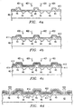
- FIGs 4a through 4d illustrate the steps for fabrication of an overcoat 31, such as that illustrated in Figure 3.
- a silicon wafer 40 having 'integrated circuits 44 patterned, including the topmost metal interconnection 45 level are positioned in a plasma enhanced chemical vapor deposition chamber.
- a standard PETEOS (plasma enhanced tetra ethyl ortho silicate) process designated by arrows 401 an oxide film 411 in the range of 5,000 to 10,000 angstroms thick is deposited.
- the gas source is changed to include silane and nitrogen and/or ammonia with the PECVD process designated by arrows 402 to deposit a film of silicon nitride 412 in the range of 1,000 to 5,000 angstroms thick.
- the nitrogen sources are removed, and in Figure 4c a final thin layer of oxide 413 is added using a standard PETEOS process 401.
- the wafer is removed from the chamber, photoresist 403 is applied and photopatterned to expose bond pads 48 and/or other openings required by the device.
- the pattern is preferably etched using a gaseous dry etching process 404 to remove the protective overcoat layers from the bond pads, and other openings on the device.
- wet etching with buffered hydrofluoric acid is used to etch the PO.
- a device having protective overcoat layers of silicon dioxide, silicon oxy-nitride, and silicon dioxide differs from that described above in that oxygen is introduced along with nitrogen, silane, and ammonia during the deposition process for the second layer.
- the processes for silicon oxy-nitride are known and used throughout the industry, in particular for E-PROM devices. Processes for the first and third layers of the overcoat are unchanged from that described above.
- Fabrication of protective overcoat of the third embodiment including a layer of silicon dioxide, silicon carbide, and silicon dioxide differs from the first embodiment in that silane/methane, trimethylsilane, tetramethylsilane, or other organosilane gas is the source gas, along with Ar or He as a carrier gas, for the second layer of silicon carbide.
- the first and third layers are of silicon dioxide using the PETEOS process.
- Plasma enhanced chemical vapor deposition (PECVD) of successive overcoat layers eliminates excessive wafer handling by sequentially depositing layered films in a single chamber.
- Processes employing plasma enhanced chemical vapor deposition provide clean, uncontaminated surfaces between the layers as a function of the atmospheric control within the chamber, thus facilitating adhesion between the multiple layers.
- PECVD optimizes process cycle time by successive depositions without handling, and by a single photopatterning step to etch openings.
- the completely inorganic overcoat of the current invention not only provides device performance advantages of enhanced adhesion to packaging polymers, but also has very high temperature stability, in excess of 450 degrees C, and has improved thermal conductivity as compared to existing enhanced surface adhesion PO technology.
- the embodiment having a silicon carbide second or barrier layer provides good thermal conductivity, and is applicable to high power circuits.
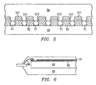
- Figure 5 illustrates a flip chip assemblage of the current invention.
- An integrated circuit device 50 having sequentially deposited protective overcoat of silicon dioxide 511, silicon nitride 512, and silicon dioxide 513 is attached to a substrate 52 using solder balls 53.
- a polymeric underfill compound 55 is completely wetted to the oxide surface 513 of the protective overcoat, and no voids resulting from poor adhesion are present in the underfill.
- FIG. 6 An alternate embodiment is illustrated in Figure 6 in a cross sectional view of a leaded plastic molded package, wherein the multilayer protective overcoat 61 of the current invention has enhanced adhesion to the molding compound 65.
- This adhesion is particularly advantageous at the corners of chip 69 where delamination of the plastic can cause shearing of the chip metal structures and /or fatigue of the bond wires.
Landscapes
- Formation Of Insulating Films (AREA)
- Structures Or Materials For Encapsulating Or Coating Semiconductor Devices Or Solid State Devices (AREA)
- Internal Circuitry In Semiconductor Integrated Circuit Devices (AREA)
Applications Claiming Priority (2)
| Application Number | Priority Date | Filing Date | Title |
|---|---|---|---|
| US21330000P | 2000-06-22 | 2000-06-22 | |
| US213300P | 2000-06-22 |
Publications (2)
| Publication Number | Publication Date |
|---|---|
| EP1168437A2 true EP1168437A2 (fr) | 2002-01-02 |
| EP1168437A3 EP1168437A3 (fr) | 2006-03-22 |
Family
ID=22794535
Family Applications (1)
| Application Number | Title | Priority Date | Filing Date |
|---|---|---|---|
| EP01202417A Withdrawn EP1168437A3 (fr) | 2000-06-22 | 2001-06-22 | Dispositif semiconduteur |
Country Status (6)
| Country | Link |
|---|---|
| US (2) | US6580170B2 (fr) |
| EP (1) | EP1168437A3 (fr) |
| JP (1) | JP2002075981A (fr) |
| KR (1) | KR20020002446A (fr) |
| CN (1) | CN1331492A (fr) |
| TW (1) | TW502377B (fr) |
Cited By (4)
| Publication number | Priority date | Publication date | Assignee | Title |
|---|---|---|---|---|
| FR2846789A1 (fr) * | 2002-11-05 | 2004-05-07 | St Microelectronics Sa | Dispositif semi-conducteur a transistors mos a couche d'arret de gravure ayant un stress residuel ameliore et procede de fabrication d'un tel dispositif semi-conducteur |
| US7026233B2 (en) | 2003-08-06 | 2006-04-11 | Taiwan Semiconductor Manufacturing Company, Ltd. | Method for reducing defects in post passivation interconnect process |
| DE102005008321A1 (de) * | 2005-02-23 | 2006-08-24 | Infineon Technologies Ag | Charge-Trapping-Halbleiterspeicherelement mit verbessertem Einfangdielektrikum |
| EP3184665A1 (fr) * | 2015-12-21 | 2017-06-28 | SPTS Technologies Limited | Procédé pour améliorer l'adhésion |
Families Citing this family (54)
| Publication number | Priority date | Publication date | Assignee | Title |
|---|---|---|---|---|
| JP3888854B2 (ja) * | 2001-02-16 | 2007-03-07 | シャープ株式会社 | 半導体集積回路の製造方法 |
| US20110213446A1 (en) * | 2001-03-02 | 2011-09-01 | Erchonia Corporation | Fungal Infection Therapy with Low Level Laser |
| US20110224759A1 (en) * | 2001-03-02 | 2011-09-15 | Erchonia Corporation | Fungal Infection Therapy with Low Level Laser |
| US20110087312A1 (en) * | 2001-03-02 | 2011-04-14 | Erchonia Corporatin | Method for Treatment of Diabetes and Prediabetes with Low-Level Laser Therapy |
| US8439959B2 (en) * | 2004-10-29 | 2013-05-14 | Erchonia Corporation | Full-body laser scanner and method of mapping and contouring the body |
| US20100016931A1 (en) * | 2001-03-02 | 2010-01-21 | Therapy Products, Inc. | Method of Reducing Cholesterol Using Laser Energy |
| ATE417021T1 (de) * | 2001-11-09 | 2008-12-15 | Wispry Inc | Mems-einrichtung mit dreischichtigem strahl und diesbezügliche verfahren |
| US7125812B2 (en) * | 2002-01-15 | 2006-10-24 | Tokyo Electron Limited | CVD method and device for forming silicon-containing insulation film |
| JP2004281248A (ja) * | 2003-03-17 | 2004-10-07 | Pioneer Electronic Corp | 耐熱絶縁フィルム及び絶縁方法 |
| US20080172045A1 (en) * | 2003-10-24 | 2008-07-17 | Shanks Steven C | Acne treatment device |
| KR20070001070A (ko) * | 2003-10-31 | 2007-01-03 | 제이에스알 가부시끼가이샤 | 적층체 및 그의 형성 방법, 절연막, 반도체 장치, 및 막형성용 조성물 |
| US7075016B2 (en) | 2004-02-18 | 2006-07-11 | Taiwan Semiconductor Manufacturing Co., Ltd. | Underfilling efficiency by modifying the substrate design of flip chips |
| US7071559B2 (en) | 2004-07-16 | 2006-07-04 | International Business Machines Corporation | Design of beol patterns to reduce the stresses on structures below chip bondpads |
| US7329620B1 (en) | 2004-10-08 | 2008-02-12 | National Semiconductor Corporation | System and method for providing an integrated circuit having increased radiation hardness and reliability |
| US20060076694A1 (en) * | 2004-10-13 | 2006-04-13 | Taiwan Semiconductor Manufacturing Co., Ltd. | Semiconductor device package with concavity-containing encapsulation body to prevent device delamination and increase thermal-transferring efficiency |
| US7223630B2 (en) * | 2004-12-03 | 2007-05-29 | Taiwan Semiconductor Manufacturing Company, Ltd. | Low stress semiconductor device coating and method of forming thereof |
| US7241693B2 (en) * | 2005-04-18 | 2007-07-10 | Macronix International Co., Ltd. | Processing method for protection of backside of a wafer |
| US7468545B2 (en) * | 2005-05-06 | 2008-12-23 | Megica Corporation | Post passivation structure for a semiconductor device and packaging process for same |
| CN100505173C (zh) * | 2005-05-16 | 2009-06-24 | 旺宏电子股份有限公司 | 化学机械研磨制程及增加其研磨终点准确性的方法 |
| FR2892562B1 (fr) * | 2005-10-21 | 2008-01-18 | Thales Sa | Dispositif de passivation d'un composant a semi-conducteur lateral |
| CN100442459C (zh) * | 2005-11-24 | 2008-12-10 | 上海华虹Nec电子有限公司 | 自对准硅化物阻挡层的制作工艺方法 |
| US7495865B2 (en) * | 2006-04-10 | 2009-02-24 | Seagate Technology Llc | Adhesion layer for protective overcoat |
| US20090104541A1 (en) * | 2007-10-23 | 2009-04-23 | Eui Kyoon Kim | Plasma surface treatment to prevent pattern collapse in immersion lithography |
| US20090132012A1 (en) * | 2007-11-16 | 2009-05-21 | Therapy Products, Inc. | Method for pretreating patient before surgery |
| US20090197086A1 (en) * | 2008-02-04 | 2009-08-06 | Sudha Rathi | Elimination of photoresist material collapse and poisoning in 45-nm feature size using dry or immersion lithography |
| JP5277746B2 (ja) * | 2008-06-20 | 2013-08-28 | 凸版印刷株式会社 | 半導体装置 |
| US20100196497A1 (en) * | 2009-02-02 | 2010-08-05 | Therapy Products, Inc. | Method of Treating Tissue Using Platelet-Rich Plasma in Combination with Low-Level Laser Therapy |
| US8478199B2 (en) * | 2009-03-30 | 2013-07-02 | Ppc Broadband, Inc. | Signal conditioning device with attenuated fail-safe bypass |
| US7944029B2 (en) * | 2009-09-16 | 2011-05-17 | Sandisk Corporation | Non-volatile memory with reduced mobile ion diffusion |
| US8563095B2 (en) * | 2010-03-15 | 2013-10-22 | Applied Materials, Inc. | Silicon nitride passivation layer for covering high aspect ratio features |
| US8741394B2 (en) * | 2010-03-25 | 2014-06-03 | Novellus Systems, Inc. | In-situ deposition of film stacks |
| US9028924B2 (en) | 2010-03-25 | 2015-05-12 | Novellus Systems, Inc. | In-situ deposition of film stacks |
| US8709551B2 (en) * | 2010-03-25 | 2014-04-29 | Novellus Systems, Inc. | Smooth silicon-containing films |
| US8846518B2 (en) | 2010-06-28 | 2014-09-30 | 3M Innovative Properties Company | Multilayer construction |
| US8252631B1 (en) * | 2011-04-28 | 2012-08-28 | Freescale Semiconductor, Inc. | Method and apparatus for integrated circuit packages using materials with low melting point |
| KR102025441B1 (ko) | 2012-04-06 | 2019-09-25 | 노벨러스 시스템즈, 인코포레이티드 | 증착 후 소프트 어닐링 |
| US9117668B2 (en) | 2012-05-23 | 2015-08-25 | Novellus Systems, Inc. | PECVD deposition of smooth silicon films |
| US9388491B2 (en) | 2012-07-23 | 2016-07-12 | Novellus Systems, Inc. | Method for deposition of conformal films with catalysis assisted low temperature CVD |
| JP6030378B2 (ja) * | 2012-08-14 | 2016-11-24 | 株式会社日立国際電気 | 半導体装置の製造方法、基板処理方法、基板処理装置およびプログラム |
| US9812338B2 (en) | 2013-03-14 | 2017-11-07 | Cree, Inc. | Encapsulation of advanced devices using novel PECVD and ALD schemes |
| US8994073B2 (en) | 2012-10-04 | 2015-03-31 | Cree, Inc. | Hydrogen mitigation schemes in the passivation of advanced devices |
| US9991399B2 (en) | 2012-10-04 | 2018-06-05 | Cree, Inc. | Passivation structure for semiconductor devices |
| US8895415B1 (en) | 2013-05-31 | 2014-11-25 | Novellus Systems, Inc. | Tensile stressed doped amorphous silicon |
| US9806043B2 (en) * | 2016-03-03 | 2017-10-31 | Infineon Technologies Ag | Method of manufacturing molded semiconductor packages having an optical inspection feature |
| CN110997975B (zh) * | 2017-07-14 | 2022-09-09 | 英福康控股股份公司 | 从部件的表面受控地除去保护层的方法 |
| DE102019101061B4 (de) | 2019-01-16 | 2022-02-17 | Infineon Technologies Ag | Verfahren zum ausbilden einer kontaktstruktur, verfahren zum ausbilden eines chipgehäuses und chipgehäuse |
| CN110212071B (zh) * | 2019-05-22 | 2020-07-07 | 华灿光电(浙江)有限公司 | 发光二极管芯片及其制作方法 |
| CN110829174A (zh) * | 2019-12-05 | 2020-02-21 | 苏州长瑞光电有限公司 | 金属与聚合物的连接方法、连接结构及半导体器件 |
| US12100634B2 (en) * | 2021-10-13 | 2024-09-24 | Nanya Technology Corporation | Semiconductor device with re-fill layer |
| CN116190457A (zh) * | 2021-11-26 | 2023-05-30 | 意法半导体股份有限公司 | 具有增强的鲁棒性的sic基电子器件及制造电子器件的方法 |
| CN114242639B (zh) * | 2021-12-14 | 2025-12-02 | 华进半导体封装先导技术研发中心有限公司 | 一种增加塑封料表面临时键合强度的键合结构和制作方法 |
| CN115172294A (zh) * | 2022-07-29 | 2022-10-11 | 晨宸辰科技有限公司 | 一种晶圆的空腔结构、构建方法及晶圆 |
| CN117334584A (zh) * | 2023-09-14 | 2024-01-02 | 中晶新源(上海)半导体有限公司 | 一种半导体器件的形成方法及半导体器件 |
| CN119161771B (zh) * | 2024-09-13 | 2025-08-08 | 广东瑞得泰科技有限公司 | 一种半导体保护膜及其涂布工艺 |
Family Cites Families (7)
| Publication number | Priority date | Publication date | Assignee | Title |
|---|---|---|---|---|
| US5244839A (en) * | 1991-06-18 | 1993-09-14 | Texas Instruments Incorporated | Semiconductor hybrids and method of making same |
| US5712206A (en) * | 1996-03-20 | 1998-01-27 | Vanguard International Semiconductor Corporation | Method of forming moisture barrier layers for integrated circuit applications |
| KR100214269B1 (ko) * | 1996-06-27 | 1999-08-02 | 김영환 | 반도체 소자의 보호막 제조방법 |
| EP0856886B1 (fr) * | 1997-01-31 | 2003-06-25 | STMicroelectronics S.r.l. | Procédé de formation d'une structure périphérique pour étancher un dispositif intégré électronique, et dispositif correspondant |
| US6368919B2 (en) * | 1999-01-19 | 2002-04-09 | Micron Technology, Inc. | Method and composite for decreasing charge leakage |
| TW444402B (en) * | 1999-03-11 | 2001-07-01 | Mosel Vitelic Inc | Flash memory cell and its manufacturing method |
| US6342428B1 (en) * | 1999-10-04 | 2002-01-29 | Philips Electronics North America Corp. | Method for a consistent shallow trench etch profile |
-
2001
- 2001-06-02 US US09/873,058 patent/US6580170B2/en not_active Expired - Lifetime
- 2001-06-13 CN CN01123308A patent/CN1331492A/zh active Pending
- 2001-06-21 KR KR1020010035383A patent/KR20020002446A/ko not_active Withdrawn
- 2001-06-22 EP EP01202417A patent/EP1168437A3/fr not_active Withdrawn
- 2001-06-22 TW TW090115185A patent/TW502377B/zh not_active IP Right Cessation
- 2001-06-22 JP JP2001189162A patent/JP2002075981A/ja not_active Abandoned
-
2003
- 2003-04-29 US US10/426,451 patent/US6787397B2/en not_active Expired - Lifetime
Cited By (8)
| Publication number | Priority date | Publication date | Assignee | Title |
|---|---|---|---|---|
| FR2846789A1 (fr) * | 2002-11-05 | 2004-05-07 | St Microelectronics Sa | Dispositif semi-conducteur a transistors mos a couche d'arret de gravure ayant un stress residuel ameliore et procede de fabrication d'un tel dispositif semi-conducteur |
| US7187038B2 (en) | 2002-11-05 | 2007-03-06 | Stmicroelectronics Sa | Semiconductor device with MOS transistors with an etch-stop layer having an improved residual stress level and method for fabricating such a semiconductor device |
| US7026233B2 (en) | 2003-08-06 | 2006-04-11 | Taiwan Semiconductor Manufacturing Company, Ltd. | Method for reducing defects in post passivation interconnect process |
| US7528478B2 (en) | 2003-08-06 | 2009-05-05 | Taiwan Semiconductor Manufacturing Company, Ltd. | Semiconductor devices having post passivation interconnections and a buffer layer |
| DE102005008321A1 (de) * | 2005-02-23 | 2006-08-24 | Infineon Technologies Ag | Charge-Trapping-Halbleiterspeicherelement mit verbessertem Einfangdielektrikum |
| DE102005008321B4 (de) * | 2005-02-23 | 2008-09-25 | Qimonda Ag | Mittels Feldeffekt steuerbares Halbleiterspeicherelement mit verbessertem Einfangdielektrikum |
| EP3184665A1 (fr) * | 2015-12-21 | 2017-06-28 | SPTS Technologies Limited | Procédé pour améliorer l'adhésion |
| US10096468B2 (en) | 2015-12-21 | 2018-10-09 | Spts Technologies Limited | Method of improving adhesion |
Also Published As
| Publication number | Publication date |
|---|---|
| KR20020002446A (ko) | 2002-01-09 |
| JP2002075981A (ja) | 2002-03-15 |
| US20020011656A1 (en) | 2002-01-31 |
| EP1168437A3 (fr) | 2006-03-22 |
| US6787397B2 (en) | 2004-09-07 |
| TW502377B (en) | 2002-09-11 |
| US6580170B2 (en) | 2003-06-17 |
| CN1331492A (zh) | 2002-01-16 |
| US20030205812A1 (en) | 2003-11-06 |
Similar Documents
| Publication | Publication Date | Title |
|---|---|---|
| US6787397B2 (en) | Semiconductor device protective overcoat with enhanced adhesion to polymeric materials and method of fabrication | |
| US6515355B1 (en) | Passivation layer for packaged integrated circuits | |
| US6972249B2 (en) | Use of nitrides for flip-chip encapsulation | |
| US6869831B2 (en) | Adhesion by plasma conditioning of semiconductor chip surfaces | |
| CN101770958B (zh) | 在芯片封装中的保护薄膜涂层 | |
| US20030038357A1 (en) | Spacer for semiconductor devices, semiconductor devices and assemblies including the spacer, and methods | |
| US20080293234A1 (en) | Semiconductor device and manufacturing method of the same | |
| US20080079176A1 (en) | Method and structure to enhance temperature/humidity/bias performance of semiconductor devices by surface modification | |
| US8053807B2 (en) | Semiconductor packages, stacked semiconductor packages, and methods of manufacturing the semiconductor packages and the stacked semiconductor packages | |
| US7374971B2 (en) | Semiconductor die edge reconditioning | |
| US7150390B2 (en) | Flip chip dip coating encapsulant | |
| US20080174002A1 (en) | Stress relieving layer for flip chip packaging | |
| US20080290513A1 (en) | Semiconductor package having molded balls and method of manufacturing the same | |
| US6852617B2 (en) | Semiconductor device fabrication method | |
| US6900080B2 (en) | Microelectronic package with reduced underfill and methods for forming such packages | |
| TW202204515A (zh) | 電子封裝件之製法及其承載結構 | |
| JP2674670B2 (ja) | 半導体装置の製造方法 | |
| CN100390970C (zh) | 提高半导体器件的温度/湿度/偏压性能的方法和结构 | |
| KR100922309B1 (ko) | 웨이퍼 레벨 반도체 패키지 제조 방법 | |
| GB2366078A (en) | Semiconductor device retaining a resist layer as a buffer layer | |
| KR20030002766A (ko) | 반도체 소자의 본드패드 개구부 형성 방법 |
Legal Events
| Date | Code | Title | Description |
|---|---|---|---|
| PUAI | Public reference made under article 153(3) epc to a published international application that has entered the european phase |
Free format text: ORIGINAL CODE: 0009012 |
|
| 17P | Request for examination filed |
Effective date: 20010622 |
|
| AK | Designated contracting states |
Kind code of ref document: A2 Designated state(s): AT BE CH CY DE DK ES FI FR GB GR IE IT LI LU MC NL PT SE TR |
|
| AX | Request for extension of the european patent |
Free format text: AL;LT;LV;MK;RO;SI |
|
| PUAL | Search report despatched |
Free format text: ORIGINAL CODE: 0009013 |
|
| AK | Designated contracting states |
Kind code of ref document: A3 Designated state(s): AT BE CH CY DE DK ES FI FR GB GR IE IT LI LU MC NL PT SE TR |
|
| AX | Request for extension of the european patent |
Extension state: AL LT LV MK RO SI |
|
| AKX | Designation fees paid |
Designated state(s): AT BE CH CY DE DK ES FI FR GB GR IE IT LI LU MC NL PT SE TR |
|
| STAA | Information on the status of an ep patent application or granted ep patent |
Free format text: STATUS: THE APPLICATION IS DEEMED TO BE WITHDRAWN |
|
| 18D | Application deemed to be withdrawn |
Effective date: 20060923 |