EP1167227A1 - Electronic parts carrier tape - Google Patents
Electronic parts carrier tape Download PDFInfo
- Publication number
- EP1167227A1 EP1167227A1 EP01115119A EP01115119A EP1167227A1 EP 1167227 A1 EP1167227 A1 EP 1167227A1 EP 01115119 A EP01115119 A EP 01115119A EP 01115119 A EP01115119 A EP 01115119A EP 1167227 A1 EP1167227 A1 EP 1167227A1
- Authority
- EP
- European Patent Office
- Prior art keywords
- carrier tape
- embossed portion
- embossed
- portions
- rib
- Prior art date
- Legal status (The legal status is an assumption and is not a legal conclusion. Google has not performed a legal analysis and makes no representation as to the accuracy of the status listed.)
- Granted
Links
- 230000002093 peripheral effect Effects 0.000 claims abstract description 27
- 238000004804 winding Methods 0.000 abstract description 4
- 238000010276 construction Methods 0.000 description 3
- 239000012050 conventional carrier Substances 0.000 description 3
- 238000012856 packing Methods 0.000 description 2
- 230000000694 effects Effects 0.000 description 1
- 239000000463 material Substances 0.000 description 1
- 238000000034 method Methods 0.000 description 1
- 239000011347 resin Substances 0.000 description 1
- 229920005989 resin Polymers 0.000 description 1
Images








Classifications
-
- H—ELECTRICITY
- H05—ELECTRIC TECHNIQUES NOT OTHERWISE PROVIDED FOR
- H05K—PRINTED CIRCUITS; CASINGS OR CONSTRUCTIONAL DETAILS OF ELECTRIC APPARATUS; MANUFACTURE OF ASSEMBLAGES OF ELECTRICAL COMPONENTS
- H05K13/00—Apparatus or processes specially adapted for manufacturing or adjusting assemblages of electric components
- H05K13/02—Feeding of components
-
- H—ELECTRICITY
- H05—ELECTRIC TECHNIQUES NOT OTHERWISE PROVIDED FOR
- H05K—PRINTED CIRCUITS; CASINGS OR CONSTRUCTIONAL DETAILS OF ELECTRIC APPARATUS; MANUFACTURE OF ASSEMBLAGES OF ELECTRICAL COMPONENTS
- H05K13/00—Apparatus or processes specially adapted for manufacturing or adjusting assemblages of electric components
- H05K13/0084—Containers and magazines for components, e.g. tube-like magazines
-
- B—PERFORMING OPERATIONS; TRANSPORTING
- B65—CONVEYING; PACKING; STORING; HANDLING THIN OR FILAMENTARY MATERIAL
- B65D—CONTAINERS FOR STORAGE OR TRANSPORT OF ARTICLES OR MATERIALS, e.g. BAGS, BARRELS, BOTTLES, BOXES, CANS, CARTONS, CRATES, DRUMS, JARS, TANKS, HOPPERS, FORWARDING CONTAINERS; ACCESSORIES, CLOSURES, OR FITTINGS THEREFOR; PACKAGING ELEMENTS; PACKAGES
- B65D73/00—Packages comprising articles attached to cards, sheets or webs
- B65D73/02—Articles, e.g. small electrical components, attached to webs
-
- B—PERFORMING OPERATIONS; TRANSPORTING
- B65—CONVEYING; PACKING; STORING; HANDLING THIN OR FILAMENTARY MATERIAL
- B65D—CONTAINERS FOR STORAGE OR TRANSPORT OF ARTICLES OR MATERIALS, e.g. BAGS, BARRELS, BOTTLES, BOXES, CANS, CARTONS, CRATES, DRUMS, JARS, TANKS, HOPPERS, FORWARDING CONTAINERS; ACCESSORIES, CLOSURES, OR FITTINGS THEREFOR; PACKAGING ELEMENTS; PACKAGES
- B65D75/00—Packages comprising articles or materials partially or wholly enclosed in strips, sheets, blanks, tubes or webs of flexible sheet material, e.g. in folded wrappers
- B65D75/28—Articles or materials wholly enclosed in composite wrappers, i.e. wrappers formed by associating or interconnecting two or more sheets or blanks
- B65D75/30—Articles or materials enclosed between two opposed sheets or blanks having their margins united, e.g. by pressure-sensitive adhesive, crimping, heat-sealing, or welding
- B65D75/32—Articles or materials enclosed between two opposed sheets or blanks having their margins united, e.g. by pressure-sensitive adhesive, crimping, heat-sealing, or welding one or both sheets or blanks being recessed to accommodate contents
- B65D75/325—Articles or materials enclosed between two opposed sheets or blanks having their margins united, e.g. by pressure-sensitive adhesive, crimping, heat-sealing, or welding one or both sheets or blanks being recessed to accommodate contents one sheet being recessed, and the other being a flat not- rigid sheet, e.g. puncturable or peelable foil
- B65D75/326—Articles or materials enclosed between two opposed sheets or blanks having their margins united, e.g. by pressure-sensitive adhesive, crimping, heat-sealing, or welding one or both sheets or blanks being recessed to accommodate contents one sheet being recessed, and the other being a flat not- rigid sheet, e.g. puncturable or peelable foil and forming one compartment
-
- B—PERFORMING OPERATIONS; TRANSPORTING
- B65—CONVEYING; PACKING; STORING; HANDLING THIN OR FILAMENTARY MATERIAL
- B65D—CONTAINERS FOR STORAGE OR TRANSPORT OF ARTICLES OR MATERIALS, e.g. BAGS, BARRELS, BOTTLES, BOXES, CANS, CARTONS, CRATES, DRUMS, JARS, TANKS, HOPPERS, FORWARDING CONTAINERS; ACCESSORIES, CLOSURES, OR FITTINGS THEREFOR; PACKAGING ELEMENTS; PACKAGES
- B65D75/00—Packages comprising articles or materials partially or wholly enclosed in strips, sheets, blanks, tubes or webs of flexible sheet material, e.g. in folded wrappers
- B65D75/28—Articles or materials wholly enclosed in composite wrappers, i.e. wrappers formed by associating or interconnecting two or more sheets or blanks
- B65D75/30—Articles or materials enclosed between two opposed sheets or blanks having their margins united, e.g. by pressure-sensitive adhesive, crimping, heat-sealing, or welding
- B65D75/32—Articles or materials enclosed between two opposed sheets or blanks having their margins united, e.g. by pressure-sensitive adhesive, crimping, heat-sealing, or welding one or both sheets or blanks being recessed to accommodate contents
- B65D75/325—Articles or materials enclosed between two opposed sheets or blanks having their margins united, e.g. by pressure-sensitive adhesive, crimping, heat-sealing, or welding one or both sheets or blanks being recessed to accommodate contents one sheet being recessed, and the other being a flat not- rigid sheet, e.g. puncturable or peelable foil
- B65D75/327—Articles or materials enclosed between two opposed sheets or blanks having their margins united, e.g. by pressure-sensitive adhesive, crimping, heat-sealing, or welding one or both sheets or blanks being recessed to accommodate contents one sheet being recessed, and the other being a flat not- rigid sheet, e.g. puncturable or peelable foil and forming several compartments
-
- H—ELECTRICITY
- H05—ELECTRIC TECHNIQUES NOT OTHERWISE PROVIDED FOR
- H05K—PRINTED CIRCUITS; CASINGS OR CONSTRUCTIONAL DETAILS OF ELECTRIC APPARATUS; MANUFACTURE OF ASSEMBLAGES OF ELECTRICAL COMPONENTS
- H05K13/00—Apparatus or processes specially adapted for manufacturing or adjusting assemblages of electric components
- H05K13/04—Mounting of components, e.g. of leadless components
- H05K13/0417—Feeding with belts or tapes
-
- B—PERFORMING OPERATIONS; TRANSPORTING
- B65—CONVEYING; PACKING; STORING; HANDLING THIN OR FILAMENTARY MATERIAL
- B65D—CONTAINERS FOR STORAGE OR TRANSPORT OF ARTICLES OR MATERIALS, e.g. BAGS, BARRELS, BOTTLES, BOXES, CANS, CARTONS, CRATES, DRUMS, JARS, TANKS, HOPPERS, FORWARDING CONTAINERS; ACCESSORIES, CLOSURES, OR FITTINGS THEREFOR; PACKAGING ELEMENTS; PACKAGES
- B65D2575/00—Packages comprising articles or materials partially or wholly enclosed in strips, sheets, blanks, tubes or webs of flexible sheet material, e.g. in folded wrappers
- B65D2575/28—Articles or materials wholly enclosed in composite wrappers, i.e. wrappers formed by association or interconnecting two or more sheets or blanks
- B65D2575/30—Articles or materials enclosed between two opposed sheets or blanks having their margins united, e.g. by pressure-sensitive adhesive, crimping, heat-sealing, or welding
- B65D2575/32—Articles or materials enclosed between two opposed sheets or blanks having their margins united, e.g. by pressure-sensitive adhesive, crimping, heat-sealing, or welding one or both sheets or blanks being recessed to accommodate contents
- B65D2575/3209—Details
- B65D2575/3218—Details with special means for gaining access to the contents
- B65D2575/3227—Cuts or weakening lines
-
- Y—GENERAL TAGGING OF NEW TECHNOLOGICAL DEVELOPMENTS; GENERAL TAGGING OF CROSS-SECTIONAL TECHNOLOGIES SPANNING OVER SEVERAL SECTIONS OF THE IPC; TECHNICAL SUBJECTS COVERED BY FORMER USPC CROSS-REFERENCE ART COLLECTIONS [XRACs] AND DIGESTS
- Y10—TECHNICAL SUBJECTS COVERED BY FORMER USPC
- Y10S—TECHNICAL SUBJECTS COVERED BY FORMER USPC CROSS-REFERENCE ART COLLECTIONS [XRACs] AND DIGESTS
- Y10S206/00—Special receptacle or package
- Y10S206/82—Separable, striplike plural articles
Definitions
- the present invention relates to an electronic parts carrier tape used for packing and transporting parts and particularly electronic parts such as IC packages.
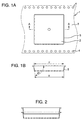
- Fig. 1 shows one known carrier tape of the type described.
- This carrier tape 1 is made of a flexible resin material, and includes recessed portions (hereinafter referred to as “embossed portions") 2 and flange portions 3.
- the plurality of embossed portions 2 are arranged at equal intervals in a longitudinal direction of the carrier tape 1, and serve to receive or store electronic parts, respectively.
- a tape-like lid member (hereinafter referred to as “cover tape”) is adhesively bonded to the flange portion 3 so that the electronic part, received in the embossed portion 2, will not drop through an opening of the embossed portion 2 during transport.
- a number of feed holes or perforations 4 are formed at equal intervals in one or both of opposite side edge portions of the carrier tape 1.
- the carrier tape 1, used for packing and transporting electronic parts, is wound on a reel after it is molded, and the carrier tape is stored in this wounded condition.
- the upper and lower embossed portions 2, superposed together, are sometimes fitted together in a nested manner (see Fig. 2).
- the conventional embossed portion has such a shape that an angle Wi of inclination of an inner surface of a side wall (peripheral wall) 5 thereof relative to the open top of the embossed portion is 75 to 89°.
- an outer dimension (X) of the bottom of the embossed portion is smaller than or generally equal to a dimension (Y) of the opening of the embossed portion, so that a nesting phenomenon, in which the superposed embossed portions are fitted together in a nested manner, is liable to occur.
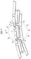
- Figs. 3 and 4 show the cross-section of the carrier tape wound on the reel.
- the embossed portions of the adjacent (inner and outer) turns of the carrier tape can be superposed together by vibrations 6, developing during the transport, a force 7 of winding of the carrier tape on the reel during the forming operation, and a pressing force 8 produced when winding the carrier tape on the reel (such a pressing force can be produced when handling the wound carrier tape), and in such a case, when there is exerted an excessive force to press the upper (outer) turn of the carrier tape against the lower (inner) turn thereof, the nesting occurs.
- the carrier tape can not be smoothly unwound from the reel during the electronic parts-mounting process, and in the worst case, the unwinding of the carrier tape is stopped, thus markedly lowering the efficiency.
- the carrier tape was forcibly unwound from the reel, there was a possibility of damaging the embossed portions.
- an electronic parts carrier tape comprising a flexible, tape-like member having electronic part-storing embossed portions arranged at predetermined intervals in a longitudinal direction of the tape-like member; wherein at least one rib is formed on and projects outwardly from an outer surface of a peripheral wall of each of the embossed portions, and an outer dimension (X) of a bottom of the embossed portion, as seen in a cross-section of the embossed portion through the rib, is larger than a dimension (Y) of an opening in a top of the embossed portion.
- the rib has a slanting portion slanting from the top of the embossed portion to the bottom thereof, and an angle Ro of inclination of an outer surface of the slanting portion of the rib relative to the top of the embossed portion is 89 to 93°.
- projections are formed respectively at corner portions of an inner bottom surface of the embossed portion, and project toward the top of the embossed portion, each of the projections having one of a flat upper surface and an inclined upper surface.
- a carrier tape used in the present invention, has a plurality of embossed portions for respectively receiving a plurality of electronic parts such as IC packages.
- IC packages includes an SOP (small Outline Package), an SSOP (Shrink Small Outline Package), a TSOP (Thin Small Outline Package), a TSSOP (Thin Shrink Small Outline Package), a PLCC (Plastic Leaded Chip Carrier), a QFP (Quad Flat Package) and a BGA (Ball Grid Allay).
- At least one rib is formed on and projects inwardly from an inner surface of a peripheral wall (side wall) of each of the embossed portions.
- 1 to 100, and more preferably 2 to 10 ribs are formed on each of four side wall portions of the peripheral wall of the embossed portion, and the ribs are arranged at a predetermined pitch, that is, at equal intervals.
- the ribs not only serve to prevent the nesting but also increase the mechanical strength of the embossed portion.
- the shape of the rib, the pitch of the ribs, the number of the ribs and so on are not limited to those described in these embodiments, but can be suitably determined in accordance with the kind of electronic parts to be received in the respective embossed portions.
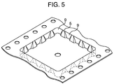
- ribs 9 are formed at equal intervals on and project outwardly from an outer surface of each of four side wall portions of a peripheral wall 5 of the embossed portion, and also similar ribs 9 are formed respectively at the four corner portions of the embossed portion, as shown in Figs. 5 and 6.
- an outer dimension (X) of the bottom of the embossed portion, as seen in a cross-section of the embossed portion through the opposite ribs 9, should be larger than a dimension (Y) of an opening in the top of the embossed portion, as shown in Fig. 6C.
- Wi 75 to 89°
- Ro 89 to 93°
- Wi ⁇ Ro ⁇ Ri is established, where Wi represents an angle of inclination of the inner surface of the peripheral wall 5 relative to the top of the embossed portion, Ri represents an angle of inclination of an inner surface of the slanting portion of the rib 9 relative to the top of the embossed portion, and Ro represents an angle of inclination of an outer surface of the slanting portion of the rib 9 relative to the top of the embossed portion.
- the embossed portion can not entirely satisfactorily hold an IC package, and besides the peripheral wall 5 is stepped too much relative to the ribs 9, so that the moldability is lowered. If Wi is more than 89°, the peripheral wall 5 is stepped little relative to the ribs 9, so that the effect of the ribs 9 is reduced. If Ro is less than 89°, the outer dimension (X) of the bottom of the embossed portion is smaller than the dimension (Y) of the opening in the top of the embossed portion, so that the nesting is liable to occur. In contrast, if Ro is more than 93°, an inverted tapering angle is obtained, so that the moldability is lowered.
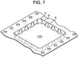
- ribs 9 are formed at equal intervals on and project outwardly from an outer surface of each of four side wall portions of a peripheral wall 5 of the embossed portion, and any such rib is not formed at each of the four corner portions of the embossed portion, as shown in Figs. 7 and 8. Requirements for preventing the nesting are the same as described above for the first embodiment.
- the shape of the ribs 9 is not particularly limited, and examples of this shape are shown in Figs. 9B, 9C and 9D, respectively.
- ribs 9 are formed at equal intervals on and project outwardly from an outer surface of each of four side wall portions of a peripheral wall 5 of the embossed portion, and also similar ribs 9 are formed respectively at the four corner portions of the embossed portion, as shown in Fig. 10. Requirements for preventing the nesting are the same as described above for the first embodiment.
- the ribs 9 are formed at equal intervals on and project outwardly from an outer surface of each of four side wall portions of the peripheral wall 5 of the embossed portion, and any such rib is not formed at each of the four corner portions of the embossed portion, as shown in Fig. 11. Requirements for preventing the nesting are the same as described above for the first embodiment.
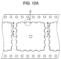
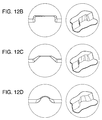
- the shape of the ribs 9 is not particularly limited, and examples of this shape are shown in Figs. 12B, 12C and 12D, respectively.
- corner portions of each electronic part can be supported by a peripheral wall of the embossed portion.
- the embossed portion need to hold the package in such a manner that a bottom surface of the package is spaced from an inner bottom surface of the embossed portion. Therefore, preferably, projections for supporting the bottom surface of the electronic part are formed respectively at the four corner portions of the inner bottom surface of the embossed portion, and project toward the open top of the embossed portion.
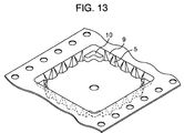
- Figs. 13 and 14 show an example in which ribs 9 are formed at equal intervals on and project outwardly from an outer surface of each of four side wall portions of a peripheral wall 5 of an embossed portion, and projections 10, each having a flat upper surface, are formed respectively at four corner portions of an inner bottom surface of the embossed portion. Requirements for preventing the nesting are the same as described above for the first embodiment.
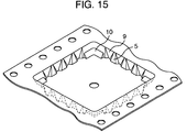
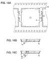
- This embodiment differs from the fifth embodiment in that an upper surface of each of projections 10, formed respectively at four corner portions of an embossed portion, is slanting.
- Fig. 17 shows an example in which ribs 9 are formed at equal intervals on and project outwardly from an outer surface of each of four side wall portions of a peripheral wall 5 of an embossed portion, and projections 10, each having a flat upper surface, are formed respectively at four corner portions of an inner bottom surface of the embossed portion, and opposite ends of each projection 10 are chamfered.
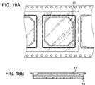
- Fig. 18 shows a condition in which a BGA 11 is received in the embossed portion.
- the BGA is supported on the projections 10.
- FIG. 19 differs from the seventh embodiment in that an upper surface of each of projections 10, formed respectively at four corner portions of an embossed portion, is slanting.
- Fig. 20 shows a condition in which a BGA 11 is received in the embossed portion. The BGA is supported on the projections 10.
- the ribs are formed on the peripheral wall of the embossed portion, and with this construction the nesting of the embossed portions is prevented.
- the ribs are formed at equal intervals on each of the four side wall portions of the peripheral wall, and with this construction the mechanical strength of the embossed portion is increased.
- the projections are formed respectively at the corner portions of the inner bottom surface of the embossed portion, and with this construction the electronic part, such as a BGA, can be held in the embossed portion in a stable manner.
Landscapes
- Engineering & Computer Science (AREA)
- Mechanical Engineering (AREA)
- Manufacturing & Machinery (AREA)
- Microelectronics & Electronic Packaging (AREA)
- Chemical & Material Sciences (AREA)
- Composite Materials (AREA)
- Packaging Frangible Articles (AREA)
- Packages (AREA)
Abstract
Description
- The present invention relates to an electronic parts carrier tape used for packing and transporting parts and particularly electronic parts such as IC packages.
- Fig. 1 shows one known carrier tape of the type described. This carrier tape 1 is made of a flexible resin material, and includes recessed portions (hereinafter referred to as "embossed portions") 2 and
flange portions 3. The plurality of embossedportions 2 are arranged at equal intervals in a longitudinal direction of the carrier tape 1, and serve to receive or store electronic parts, respectively. A tape-like lid member (hereinafter referred to as "cover tape") is adhesively bonded to theflange portion 3 so that the electronic part, received in the embossedportion 2, will not drop through an opening of the embossedportion 2 during transport. A number of feed holes orperforations 4 are formed at equal intervals in one or both of opposite side edge portions of the carrier tape 1. - The carrier tape 1, used for packing and transporting electronic parts, is wound on a reel after it is molded, and the carrier tape is stored in this wounded condition. At this time, the upper and lower embossed
portions 2, superposed together, are sometimes fitted together in a nested manner (see Fig. 2). The conventional embossed portion has such a shape that an angle Wi of inclination of an inner surface of a side wall (peripheral wall) 5 thereof relative to the open top of the embossed portion is 75 to 89°. Therefore, an outer dimension (X) of the bottom of the embossed portion is smaller than or generally equal to a dimension (Y) of the opening of the embossed portion, so that a nesting phenomenon, in which the superposed embossed portions are fitted together in a nested manner, is liable to occur. - Figs. 3 and 4 show the cross-section of the carrier tape wound on the reel. The embossed portions of the adjacent (inner and outer) turns of the carrier tape can be superposed together by vibrations 6, developing during the transport, a
force 7 of winding of the carrier tape on the reel during the forming operation, and a pressing force 8 produced when winding the carrier tape on the reel (such a pressing force can be produced when handling the wound carrier tape), and in such a case, when there is exerted an excessive force to press the upper (outer) turn of the carrier tape against the lower (inner) turn thereof, the nesting occurs. - When the nesting occurs, the carrier tape can not be smoothly unwound from the reel during the electronic parts-mounting process, and in the worst case, the unwinding of the carrier tape is stopped, thus markedly lowering the efficiency. When the carrier tape was forcibly unwound from the reel, there was a possibility of damaging the embossed portions.
- It is an object of the present invention to provide an electronic parts carrier tape in which a nesting phenomenon, in which superposed embossed portions are fitted together after winding the carrier tape on a reel, is less liable to occur.
- According to the feature of the present invention, there is provided an electronic parts carrier tape comprising a flexible, tape-like member having electronic part-storing embossed portions arranged at predetermined intervals in a longitudinal direction of the tape-like member;
wherein at least one rib is formed on and projects outwardly from an outer surface of a peripheral wall of each of the embossed portions, and an outer dimension (X) of a bottom of the embossed portion, as seen in a cross-section of the embossed portion through the rib, is larger than a dimension (Y) of an opening in a top of the embossed portion. - As a preferred embodiment of the present invention, the rib has a slanting portion slanting from the top of the embossed portion to the bottom thereof, and an angle Ro of inclination of an outer surface of the slanting portion of the rib relative to the top of the embossed portion is 89 to 93°.
- Preferably, according to the present invention, projections are formed respectively at corner portions of an inner bottom surface of the embossed portion, and project toward the top of the embossed portion, each of the projections having one of a flat upper surface and an inclined upper surface.
-
- Fig. 1A is a plan view of a conventional carrier tape;
- Figs. 1B is a cross-sectional view taken along the line A-A of Fig. 1A;
- Fig. 2 is a cross-sectional view showing the conventional carrier tape in a nested condition;
- Fig. 3 is a cross-sectional view showing the conventional carrier tape in a nested condition;
- Fig. 4 is an enlarged view of a portion of the carrier tape of Fig. 3;
- Fig. 5 is a perspective view of a first embodiment of a carrier tape of the present invention;
- Fig. 6A is a plan view of the carrier tape of the first embodiment;
- Fig. 6B is a cross-sectional view taken along the line A-A of Fig. 6A;
- Fig. 6C is a cross-sectional view taken along the line B-B of Fig. 6A;
- Fig. 7 is a perspective view of a second embodiment of a carrier tape of the present invention;
- Fig. 8A is a plan view of the carrier tape of the second embodiment;
- Fig. 8B is a cross-sectional view taken along the line A-A of Fig. 8A;
- Fig. 8C is a cross-sectional view taken along the line B-B of Fig. 8A;
- Fig. 9A is a plan view of the carrier tape of the second embodiment;
- Fig. 9B is an enlarged, schematic view showing one example of a portion C of Fig. 9A;
- Fig. 9C is an enlarged, schematic view showing another example of the portion C of Fig. 9A;
- Fig. 9D is an enlarged, schematic view showing a further example of the portion C of Fig. 9A;
- Fig. 10A is a plan view of a third embodiment of a carrier tape of the invention;
- Fig. 10B is a cross-sectional view taken along the line A-A of Fig. 10A;
- Fig. 10C is a cross-sectional view taken along the line B-B of Fig. 10A;
- Fig. 11A is a plan view of a fourth embodiment of a carrier tape of the invention;
- Fig. 11B is a cross-sectional view taken along the line A-A of Fig. 11A;
- Fig. 11C is a cross-sectional view taken along the line B-B of Fig. 11A;
- Fig. 12A is a plan view of the carrier tape of the fourth embodiment;
- Fig. 12B is an enlarged, schematic view showing one example of a portion C of Fig. 12A;
- Fig. 12C is an enlarged, schematic view showing another example of the portion C of Fig. 12A;
- Fig. 12D is an enlarged, schematic view showing a further example of the portion C of Fig. 12A;
- Fig. 13 is a perspective view of a fifth embodiment of a carrier tape of the invention;
- Fig. 14A is a plan view of the carrier tape of the fifth embodiment;
- Fig. 14B is a cross-sectional view taken along the line A-A of Fig. 14A;
- Fig. 14C is a cross-sectional view taken along the line B-B of Fig. 14A;
- Fig. 15 is a perspective view of a sixth embodiment of a carrier tape of the present invention;
- Fig. 16A is a plan view of the carrier tape of the sixth embodiment;
- Fig. 16B is a cross-sectional view taken along the line A-A of Fig. 16A;
- Fig. 16C is a cross-sectional view taken along the line B-B of Fig. 16A;
- Fig. 17A is a plan view of a seventh embodiment of a carrier tape of the invention;
- Fig. 17B is a cross-sectional view taken along the line A-A of Fig. 17A;
- Fig. 17C is a cross-sectional view taken along the line B-B of Fig. 17A;
- Fig. 18A is a plan view of the carrier tape of the seventh embodiment storing BGAs;
- Fig. 18B is a cross-sectional view taken along the line C-C of Fig. 18A;
- Fig. 19A is a plan view of an eighth embodiment of a carrier tape of the invention;
- Fig. 19B is a cross-sectional view taken along the line A-A of Fig. 19A;
- Fig. 19C is a cross-sectional view taken along the line B-B of Fig. 19A;
- Fig. 20A is a plan view of the carrier tape of the eighth embodiment storing BGAs; and
- Fig. 20B is a cross-sectional view taken along the line C-C of Fig. 20A.
-
- A carrier tape, used in the present invention, has a plurality of embossed portions for respectively receiving a plurality of electronic parts such as IC packages. Examples of such IC packages includes an SOP (small Outline Package), an SSOP (Shrink Small Outline Package), a TSOP (Thin Small Outline Package), a TSSOP (Thin Shrink Small Outline Package), a PLCC (Plastic Leaded Chip Carrier), a QFP (Quad Flat Package) and a BGA (Ball Grid Allay).
- In the carrier tape of the present invention, at least one rib is formed on and projects inwardly from an inner surface of a peripheral wall (side wall) of each of the embossed portions. Preferably, 1 to 100, and more preferably 2 to 10 ribs are formed on each of four side wall portions of the peripheral wall of the embossed portion, and the ribs are arranged at a predetermined pitch, that is, at equal intervals. With this arrangement, the ribs not only serve to prevent the nesting but also increase the mechanical strength of the embossed portion.
- Preferred Embodiments of the present invention will now be described with reference to the drawings. The shape of the rib, the pitch of the ribs, the number of the ribs and so on are not limited to those described in these embodiments, but can be suitably determined in accordance with the kind of electronic parts to be received in the respective embossed portions.
- In the case where it is necessary that the electronic part to be received in an embossed portion should not be positively held by corner portions of the embossed portion, preferably,
ribs 9 are formed at equal intervals on and project outwardly from an outer surface of each of four side wall portions of aperipheral wall 5 of the embossed portion, and alsosimilar ribs 9 are formed respectively at the four corner portions of the embossed portion, as shown in Figs. 5 and 6. - Here, in order to prevent the nesting, it is necessary that an outer dimension (X) of the bottom of the embossed portion, as seen in a cross-section of the embossed portion through the
opposite ribs 9, should be larger than a dimension (Y) of an opening in the top of the embossed portion, as shown in Fig. 6C. In the case where the uppermost portions (upper ends) of theribs 9 are disposed at the uppermost portion (upper edge portion) of the peripheral wall, and therib 9 has a slanting portion slanting from the top of the embossed portion to the bottom thereof, preferably, Wi is 75 to 89°, Ro is 89 to 93°, and Wi < Ro ≤ Ri is established, where Wi represents an angle of inclination of the inner surface of theperipheral wall 5 relative to the top of the embossed portion, Ri represents an angle of inclination of an inner surface of the slanting portion of therib 9 relative to the top of the embossed portion, and Ro represents an angle of inclination of an outer surface of the slanting portion of therib 9 relative to the top of the embossed portion. If Wi is less than 75°, the embossed portion can not entirely satisfactorily hold an IC package, and besides theperipheral wall 5 is stepped too much relative to theribs 9, so that the moldability is lowered. If Wi is more than 89°, theperipheral wall 5 is stepped little relative to theribs 9, so that the effect of theribs 9 is reduced. If Ro is less than 89°, the outer dimension (X) of the bottom of the embossed portion is smaller than the dimension (Y) of the opening in the top of the embossed portion, so that the nesting is liable to occur. In contrast, if Ro is more than 93°, an inverted tapering angle is obtained, so that the moldability is lowered. If Ro ≤ Wi is provided, it is difficult to form the ribs projecting outwardly from the outer surface of theperipheral wall 5 of the embossed portion. If Ro > Ri is provided, it is possible that the thickness of the upper portion of theperipheral wall 5 is extremely small, so that the strength of a pocket portion is reduced. - In the case where it is necessary that the electronic part should be positively held by corner portions of an embossed portion, preferably,
ribs 9 are formed at equal intervals on and project outwardly from an outer surface of each of four side wall portions of aperipheral wall 5 of the embossed portion, and any such rib is not formed at each of the four corner portions of the embossed portion, as shown in Figs. 7 and 8. Requirements for preventing the nesting are the same as described above for the first embodiment. In the case where the uppermost portions of therib 9 are disposed at the uppermost portion of theperipheral wall 5, the shape of theribs 9 is not particularly limited, and examples of this shape are shown in Figs. 9B, 9C and 9D, respectively. - Uppermost portions of ribs do not need to be disposed at an uppermost portion (upper edge portion) of a peripheral wall of an embossed portion, but may be offset outwardly from the uppermost portion of the peripheral wall. In the case where it is necessary that the electronic part should not be positively held by corner portions of the embossed portion,
ribs 9 are formed at equal intervals on and project outwardly from an outer surface of each of four side wall portions of aperipheral wall 5 of the embossed portion, and alsosimilar ribs 9 are formed respectively at the four corner portions of the embossed portion, as shown in Fig. 10. Requirements for preventing the nesting are the same as described above for the first embodiment. - In the case where ribs are stepped relative to a peripheral wall of an embossed portion, and it is necessary that the electronic part should be held by corner portions of the embossed portion, the
ribs 9 are formed at equal intervals on and project outwardly from an outer surface of each of four side wall portions of theperipheral wall 5 of the embossed portion, and any such rib is not formed at each of the four corner portions of the embossed portion, as shown in Fig. 11. Requirements for preventing the nesting are the same as described above for the first embodiment. - In the case where the uppermost portions of the
ribs 9 are not disposed at the uppermost portion (upper edge portion) of theperipheral wall 5, but are offset outwardly from the uppermost portion of theperipheral wall 5, the shape of theribs 9 is not particularly limited, and examples of this shape are shown in Figs. 12B, 12C and 12D, respectively. - In the case of holding electronic parts by embossed portions of a carrier tape, respectively, corner portions of each electronic part can be supported by a peripheral wall of the embossed portion. In the case where packages to be held by the embossed portions are BGAs or the like, the embossed portion need to hold the package in such a manner that a bottom surface of the package is spaced from an inner bottom surface of the embossed portion. Therefore, preferably, projections for supporting the bottom surface of the electronic part are formed respectively at the four corner portions of the inner bottom surface of the embossed portion, and project toward the open top of the embossed portion.
- Figs. 13 and 14 show an example in which
ribs 9 are formed at equal intervals on and project outwardly from an outer surface of each of four side wall portions of aperipheral wall 5 of an embossed portion, andprojections 10, each having a flat upper surface, are formed respectively at four corner portions of an inner bottom surface of the embossed portion. Requirements for preventing the nesting are the same as described above for the first embodiment. - This embodiment, shown in Figs. 15 and 16, differs from the fifth embodiment in that an upper surface of each of
projections 10, formed respectively at four corner portions of an embossed portion, is slanting. - Fig. 17 shows an example in which
ribs 9 are formed at equal intervals on and project outwardly from an outer surface of each of four side wall portions of aperipheral wall 5 of an embossed portion, andprojections 10, each having a flat upper surface, are formed respectively at four corner portions of an inner bottom surface of the embossed portion, and opposite ends of eachprojection 10 are chamfered. - Fig. 18 shows a condition in which a
BGA 11 is received in the embossed portion. The BGA is supported on theprojections 10. - This embodiment, shown in Fig. 19, differs from the seventh embodiment in that an upper surface of each of
projections 10, formed respectively at four corner portions of an embossed portion, is slanting. Fig. 20 shows a condition in which aBGA 11 is received in the embossed portion. The BGA is supported on theprojections 10. - In the present invention, the ribs are formed on the peripheral wall of the embossed portion, and with this construction the nesting of the embossed portions is prevented. The ribs are formed at equal intervals on each of the four side wall portions of the peripheral wall, and with this construction the mechanical strength of the embossed portion is increased.
- Further, the projections are formed respectively at the corner portions of the inner bottom surface of the embossed portion, and with this construction the electronic part, such as a BGA, can be held in the embossed portion in a stable manner.
Claims (3)
- An electronic parts carrier tape comprising a flexible, tape-like member having electronic part-storing embossed portions arranged at predetermined intervals in a longitudinal direction of said tape-like member;
wherein at least one rib is formed on and projects outwardly from an outer surface of a peripheral wall of each of said embossed portions, and an outer dimension (X) of a bottom of said embossed portion, as seen in a cross-section of said embossed portion through said rib, is larger than a dimension (Y) of an opening in a top of said embossed portion. - An electronic parts carrier tape according to claim 1, in which said rib has a slanting portion slanting from the top of said embossed portion to the bottom thereof, and an angle Ro of inclination of an outer surface of said slanting portion of said rib relative to the top of said embossed portion is 89 to 93°.
- An electronic parts carrier tape according to Claims 1 or 2, in which projections are formed respectively at corner portions of an inner bottom surface of said embossed portion, and project toward the top of said embossed portion, each of said projections having one of a flat upper surface and an inclined upper surface.
Applications Claiming Priority (2)
| Application Number | Priority Date | Filing Date | Title |
|---|---|---|---|
| SG200003550 | 2000-06-23 | ||
| SG2000035501 | 2000-06-23 |
Publications (2)
| Publication Number | Publication Date |
|---|---|
| EP1167227A1 true EP1167227A1 (en) | 2002-01-02 |
| EP1167227B1 EP1167227B1 (en) | 2003-12-17 |
Family
ID=78414122
Family Applications (1)
| Application Number | Title | Priority Date | Filing Date |
|---|---|---|---|
| EP01115119A Expired - Lifetime EP1167227B1 (en) | 2000-06-23 | 2001-06-21 | Electronic parts carrier tape |
Country Status (7)
| Country | Link |
|---|---|
| US (1) | US6729474B2 (en) |
| EP (1) | EP1167227B1 (en) |
| JP (1) | JP2002046770A (en) |
| KR (1) | KR100681742B1 (en) |
| CN (1) | CN1199827C (en) |
| DE (1) | DE60101505T2 (en) |
| MY (1) | MY126840A (en) |
Cited By (1)
| Publication number | Priority date | Publication date | Assignee | Title |
|---|---|---|---|---|
| EP1777172A3 (en) * | 2005-10-19 | 2007-06-27 | Manfred Jacob Kunststofftechnik GmbH | Container for electronic components and use thereof |
Families Citing this family (15)
| Publication number | Priority date | Publication date | Assignee | Title |
|---|---|---|---|---|
| JP3957553B2 (en) * | 2002-04-19 | 2007-08-15 | 株式会社リコー | Carrier tape for storing small articles, storage device and transport method |
| WO2003093139A1 (en) * | 2002-05-01 | 2003-11-13 | Entegris, Inc. | Carrier tape for electronic components |
| JP2005047565A (en) * | 2003-07-29 | 2005-02-24 | Sumitomo Bakelite Co Ltd | Embossed carrier tape with electronic component stored therein |
| US7407359B2 (en) * | 2005-05-27 | 2008-08-05 | Danville Automation Holdings Llc | Funnel plate |
| US20070074996A1 (en) * | 2005-10-05 | 2007-04-05 | Nice Travis S | Carrier tape and heat shrinking cover tape for integrated circuit devices |
| CN2848742Y (en) * | 2005-11-26 | 2006-12-20 | 富士康(昆山)电脑接插件有限公司 | Package carrier belt |
| JP4716928B2 (en) * | 2006-06-07 | 2011-07-06 | 信越ポリマー株式会社 | Wafer storage container |
| JP2008273578A (en) * | 2007-04-27 | 2008-11-13 | Koa Corp | Packaging tape and electronic component for surface mounting |
| US9048272B2 (en) * | 2008-09-25 | 2015-06-02 | Illinois Tool Works Inc. | Devices and method for handling microelectronics assemblies |
| CN101830316A (en) * | 2010-03-10 | 2010-09-15 | 江阴新杰科技有限公司 | Electronic package carrier tape |
| USD695635S1 (en) * | 2010-08-06 | 2013-12-17 | Murata Manufacturing Co., Ltd. | Carrier tape |
| US20170166373A1 (en) * | 2014-07-29 | 2017-06-15 | Sekisui Chemical Co., Ltd. | Film molded article, film packaged body using the same, manufacturing method for film molded article and manufacturing method for film packaged body |
| WO2018161250A1 (en) * | 2017-03-07 | 2018-09-13 | 3M Innovative Properties Company | Carrier tape having anti-nesting features |
| USD871233S1 (en) * | 2018-02-12 | 2019-12-31 | Advantek, Inc. | Carrier tape |
| USD876963S1 (en) * | 2018-03-30 | 2020-03-03 | Advantek, Inc. | Carrier tape |
Citations (3)
| Publication number | Priority date | Publication date | Assignee | Title |
|---|---|---|---|---|
| US4966281A (en) * | 1988-09-09 | 1990-10-30 | Nitto Denko Corporation | Electronic component carrier |
| EP0399784A1 (en) * | 1989-05-25 | 1990-11-28 | Minnesota Mining And Manufacturing Company | Non nesting component carrier tape |
| EP0522680A1 (en) * | 1991-07-08 | 1993-01-13 | Advantek, Inc. | Micro-chip storage tape |
Family Cites Families (11)
| Publication number | Priority date | Publication date | Assignee | Title |
|---|---|---|---|---|
| JPS6151896A (en) * | 1984-08-21 | 1986-03-14 | 株式会社村田製作所 | Electronic part series |
| US5351821A (en) * | 1992-04-30 | 1994-10-04 | Minnesota Mining And Manufacturing Company | Carrier tape with generic pockets |
| US5472085A (en) * | 1994-05-16 | 1995-12-05 | Gpax International, Inc. | Gated-pocket tape-form packaging system |
| JPH08230938A (en) | 1995-02-28 | 1996-09-10 | Mitsumi Electric Co Ltd | Embossed carrier tape |
| US5664680A (en) * | 1996-04-09 | 1997-09-09 | Caritech Inc. | Pockets for microchip carriers |
| US6016917A (en) * | 1997-04-24 | 2000-01-25 | Peak International, Inc. | Component carrier having a pocket including a pedestal |
| US6102210A (en) * | 1997-10-27 | 2000-08-15 | Sumitomo Bakelite Company Limited | Carrier tape for electronic components |
| US5967328A (en) * | 1998-01-22 | 1999-10-19 | Dial Tool Industries, Inc. | Part carrier strip |
| US6016918A (en) * | 1998-08-18 | 2000-01-25 | Dial Tool Industries, Inc. | Part carrier strip |
| US6047832A (en) * | 1999-08-13 | 2000-04-11 | Advantek, Inc. | Component carrier tape |
| US6293404B1 (en) * | 2000-02-23 | 2001-09-25 | Advantek, Inc. | Non-nesting component carrier tape |
-
2001
- 2001-06-14 MY MYPI20012802 patent/MY126840A/en unknown
- 2001-06-18 US US09/882,300 patent/US6729474B2/en not_active Expired - Fee Related
- 2001-06-21 DE DE60101505T patent/DE60101505T2/en not_active Expired - Lifetime
- 2001-06-21 EP EP01115119A patent/EP1167227B1/en not_active Expired - Lifetime
- 2001-06-22 JP JP2001189139A patent/JP2002046770A/en active Pending
- 2001-06-22 KR KR1020010035754A patent/KR100681742B1/en not_active Expired - Fee Related
- 2001-06-25 CN CNB011219351A patent/CN1199827C/en not_active Expired - Fee Related
Patent Citations (3)
| Publication number | Priority date | Publication date | Assignee | Title |
|---|---|---|---|---|
| US4966281A (en) * | 1988-09-09 | 1990-10-30 | Nitto Denko Corporation | Electronic component carrier |
| EP0399784A1 (en) * | 1989-05-25 | 1990-11-28 | Minnesota Mining And Manufacturing Company | Non nesting component carrier tape |
| EP0522680A1 (en) * | 1991-07-08 | 1993-01-13 | Advantek, Inc. | Micro-chip storage tape |
Cited By (1)
| Publication number | Priority date | Publication date | Assignee | Title |
|---|---|---|---|---|
| EP1777172A3 (en) * | 2005-10-19 | 2007-06-27 | Manfred Jacob Kunststofftechnik GmbH | Container for electronic components and use thereof |
Also Published As
| Publication number | Publication date |
|---|---|
| KR100681742B1 (en) | 2007-02-15 |
| MY126840A (en) | 2006-10-31 |
| JP2002046770A (en) | 2002-02-12 |
| EP1167227B1 (en) | 2003-12-17 |
| KR20020000521A (en) | 2002-01-05 |
| US6729474B2 (en) | 2004-05-04 |
| CN1199827C (en) | 2005-05-04 |
| DE60101505D1 (en) | 2004-01-29 |
| CN1330028A (en) | 2002-01-09 |
| US20020017478A1 (en) | 2002-02-14 |
| DE60101505T2 (en) | 2004-09-23 |
Similar Documents
| Publication | Publication Date | Title |
|---|---|---|
| EP1167227B1 (en) | Electronic parts carrier tape | |
| US7021467B2 (en) | Carrier tape for containing good therein, and container using the carrier tape | |
| US20040232037A1 (en) | Embossed carrier tape for electronic devices | |
| US7395932B2 (en) | Carrier tape for electronic components | |
| JP3012490U (en) | Carrier tape | |
| JP2003072835A (en) | Electronic component carrier tape and electronic component mounting method | |
| US6892886B2 (en) | Carrier tape with reinforced restraining member | |
| JPH08198318A (en) | Component package | |
| JP4124516B2 (en) | Carrier tape | |
| JPH02258573A (en) | carrier tape | |
| JP3907240B2 (en) | Carrier tape | |
| JP2004137080A (en) | Method for winding carrier tape | |
| JP2007230633A (en) | Electronic component storage container | |
| JPH07149393A (en) | Electronic component carrier tape | |
| JP7597059B2 (en) | Electronic component packaging | |
| US7694825B1 (en) | Carrier tape for electronic components | |
| JP2002211680A (en) | Semiconductor storage device | |
| JP4933820B2 (en) | Storage tray | |
| JPH05330745A (en) | Reel for winding carrier tape | |
| JPH10101179A (en) | Part package | |
| US20030106833A1 (en) | Carrier tape with reinforcing | |
| JP2003212290A (en) | Carrier tape for parts | |
| TWI759439B (en) | Carrier tape having anti-nesting features | |
| JP2841848B2 (en) | Leadframe storage | |
| KR20020060306A (en) | Tray for pin grid array packages having protection part |
Legal Events
| Date | Code | Title | Description |
|---|---|---|---|
| PUAI | Public reference made under article 153(3) epc to a published international application that has entered the european phase |
Free format text: ORIGINAL CODE: 0009012 |
|
| AK | Designated contracting states |
Kind code of ref document: A1 Designated state(s): AT BE CH CY DE DK ES FI FR GB GR IE IT LI LU MC NL PT SE TR Kind code of ref document: A1 Designated state(s): DE FR GB |
|
| AX | Request for extension of the european patent |
Free format text: AL;LT;LV;MK;RO;SI |
|
| 17P | Request for examination filed |
Effective date: 20020621 |
|
| AKX | Designation fees paid |
Free format text: DE FR GB |
|
| 17Q | First examination report despatched |
Effective date: 20021030 |
|
| GRAH | Despatch of communication of intention to grant a patent |
Free format text: ORIGINAL CODE: EPIDOS IGRA |
|
| GRAS | Grant fee paid |
Free format text: ORIGINAL CODE: EPIDOSNIGR3 |
|
| GRAA | (expected) grant |
Free format text: ORIGINAL CODE: 0009210 |
|
| AK | Designated contracting states |
Kind code of ref document: B1 Designated state(s): DE FR GB |
|
| REG | Reference to a national code |
Ref country code: GB Ref legal event code: FG4D |
|
| REG | Reference to a national code |
Ref country code: IE Ref legal event code: FG4D |
|
| REF | Corresponds to: |
Ref document number: 60101505 Country of ref document: DE Date of ref document: 20040129 Kind code of ref document: P |
|
| ET | Fr: translation filed | ||
| PLBE | No opposition filed within time limit |
Free format text: ORIGINAL CODE: 0009261 |
|
| STAA | Information on the status of an ep patent application or granted ep patent |
Free format text: STATUS: NO OPPOSITION FILED WITHIN TIME LIMIT |
|
| 26N | No opposition filed |
Effective date: 20040920 |
|
| REG | Reference to a national code |
Ref country code: IE Ref legal event code: MM4A |
|
| PGFP | Annual fee paid to national office [announced via postgrant information from national office to epo] |
Ref country code: DE Payment date: 20130619 Year of fee payment: 13 Ref country code: GB Payment date: 20130619 Year of fee payment: 13 |
|
| PGFP | Annual fee paid to national office [announced via postgrant information from national office to epo] |
Ref country code: FR Payment date: 20130624 Year of fee payment: 13 |
|
| REG | Reference to a national code |
Ref country code: DE Ref legal event code: R119 Ref document number: 60101505 Country of ref document: DE |
|
| GBPC | Gb: european patent ceased through non-payment of renewal fee |
Effective date: 20140621 |
|
| REG | Reference to a national code |
Ref country code: FR Ref legal event code: ST Effective date: 20150227 |
|
| REG | Reference to a national code |
Ref country code: DE Ref legal event code: R119 Ref document number: 60101505 Country of ref document: DE Effective date: 20150101 |
|
| PG25 | Lapsed in a contracting state [announced via postgrant information from national office to epo] |
Ref country code: DE Free format text: LAPSE BECAUSE OF NON-PAYMENT OF DUE FEES Effective date: 20150101 |
|
| PG25 | Lapsed in a contracting state [announced via postgrant information from national office to epo] |
Ref country code: GB Free format text: LAPSE BECAUSE OF NON-PAYMENT OF DUE FEES Effective date: 20140621 Ref country code: FR Free format text: LAPSE BECAUSE OF NON-PAYMENT OF DUE FEES Effective date: 20140630 |