EP1163573B1 - Arbitration methods and systems for arbitrating access to a disk controller memory - Google Patents
Arbitration methods and systems for arbitrating access to a disk controller memory Download PDFInfo
- Publication number
- EP1163573B1 EP1163573B1 EP00918322A EP00918322A EP1163573B1 EP 1163573 B1 EP1163573 B1 EP 1163573B1 EP 00918322 A EP00918322 A EP 00918322A EP 00918322 A EP00918322 A EP 00918322A EP 1163573 B1 EP1163573 B1 EP 1163573B1
- Authority
- EP
- European Patent Office
- Prior art keywords
- access
- time
- amount
- unit
- duration
- Prior art date
- Legal status (The legal status is an assumption and is not a legal conclusion. Google has not performed a legal analysis and makes no representation as to the accuracy of the status listed.)
- Expired - Lifetime
Links
Images


Classifications
-
- G—PHYSICS
- G06—COMPUTING OR CALCULATING; COUNTING
- G06F—ELECTRIC DIGITAL DATA PROCESSING
- G06F3/00—Input arrangements for transferring data to be processed into a form capable of being handled by the computer; Output arrangements for transferring data from processing unit to output unit, e.g. interface arrangements
- G06F3/06—Digital input from, or digital output to, record carriers, e.g. RAID, emulated record carriers or networked record carriers
- G06F3/0601—Interfaces specially adapted for storage systems
- G06F3/0602—Interfaces specially adapted for storage systems specifically adapted to achieve a particular effect
- G06F3/061—Improving I/O performance
- G06F3/0613—Improving I/O performance in relation to throughput
-
- G—PHYSICS
- G06—COMPUTING OR CALCULATING; COUNTING
- G06F—ELECTRIC DIGITAL DATA PROCESSING
- G06F3/00—Input arrangements for transferring data to be processed into a form capable of being handled by the computer; Output arrangements for transferring data from processing unit to output unit, e.g. interface arrangements
- G06F3/06—Digital input from, or digital output to, record carriers, e.g. RAID, emulated record carriers or networked record carriers
- G06F3/0601—Interfaces specially adapted for storage systems
- G06F3/0628—Interfaces specially adapted for storage systems making use of a particular technique
- G06F3/0655—Vertical data movement, i.e. input-output transfer; data movement between one or more hosts and one or more storage devices
- G06F3/0656—Data buffering arrangements
-
- G—PHYSICS
- G06—COMPUTING OR CALCULATING; COUNTING
- G06F—ELECTRIC DIGITAL DATA PROCESSING
- G06F3/00—Input arrangements for transferring data to be processed into a form capable of being handled by the computer; Output arrangements for transferring data from processing unit to output unit, e.g. interface arrangements
- G06F3/06—Digital input from, or digital output to, record carriers, e.g. RAID, emulated record carriers or networked record carriers
- G06F3/0601—Interfaces specially adapted for storage systems
- G06F3/0668—Interfaces specially adapted for storage systems adopting a particular infrastructure
- G06F3/0671—In-line storage system
- G06F3/0673—Single storage device
- G06F3/0674—Disk device
Definitions
- the present invention relates to mass data storage device controllers. More particularly, the invention relates to methods and systems for arbitrating access to a disk controller memory.
- Mass data storage is a critical component of computer systems. Typically, mass storage units consist of nonvolatile memory such as a hard disk, an optical drive or other type of storage device. Computer systems typically also contain volatile system memory, such as random access memory (RAM) circuits. Most personal computers today contain less than 256 megabytes of RAM while the same computers often contain hard disks with up to 10 gigabytes or more of capacity.
- RAM random access memory
- the mass storage unit of a computer is used to store programs and data on a nonvolatile basis.
- the mass storage device retains data even when the computer and the mass storage device are powered down.
- Volatile system memory serves as a temporary repository of program code and data.
- volatile system memory can be accessed much more quickly than a mass storage device.
- a mass storage unit typically consists of a hard disk and a hard disk controller (HDC).
- the controller operates the hard disk, formats data as it is written to the disk, checks data as it is read from the disk, communicates the data to and from a host system, and buffers the data so as to compensate for latency and difference in data transfer rates between the hard disk and the host computer system.
- the HDC includes a buffer memory which may be used to buffer data between the disk and the host. Because several functional units, such as the disk, the host, and the local controller, need to interact with the buffer memory, access to the buffer memory must be coordinated in some manner. Thus, the HDC may utilize an access arbiter to negotiate access to the buffer memory among various devices requesting access. However, conventional systems typically utilize arbiters that inefficiently provide fixed amounts of access times to accessing units each access cycle. Thus, conventional systems fail to dynamically accommodate changing utilizations of the buffer memory by the accessing units.
- the HDC includes a buffer memory which may be used to buffer data between the disk and the host. Because several functional units, such as the disk, the host, and the local controller, need to interact with the buffer memory, access to the buffer memory must be coordinated in some manner. Thus, the HDC may utilize an access arbiter to negotiate access to the buffer memory among various devices requesting access. However, conventional systems typically utilize arbiters that inefficiently provide fixed amounts of access times to accessing units each access cycle. Thus, conventional systems fail to dynamically accommodate changing utilizations of the buffer memory by the accessing units.
- EP-A-0 622 726 discloses a method for arbitrating the access of multiple accessing units to a shared buffer memory in a mass storage device controller.
- an improved disk drive architecture includes a microcontroller interface circuit connected between a drive microcontroller and a buffer controller.
- the microcontroller interface circuit includes address mapping registers for mapping at least one predetermined portion of directly addressable memory of the microcontroller to address locations of the drive's cache buffer.
- the buffer controller circuit includes an access arbitration circuit for arbitrating requests for access to the cache buffer by the drive's data sequencer, the drive's host interface controller and the drive's microcontroller.
- a microcontroller wait state generator responds to the access arbitration circuit by generating and applying a wait state sequence to the microcontroller until a request it makes for access to the cache buffer can be executed.
- the present invention discloses a method and system for arbitrating access to a shared resource of a mass storage device controller.
- the controller is a hard disk controller and the shared resource is a local buffer memory of the hard disk controller.
- Several units or circuits within the controller each access the buffer memory to store or retrieve information. These units may include a controller microprocessor, a host interface unit, a disk formatter unit, a buffer memory refresh unit, a disk format data fetch unit, and an error correction unit.
- the various access requirements of the units are taken into account.
- the disk controller has the most time critical, predictable and periodic access requirements
- the other units have less critical and less predictable access requirements
- the host interface unit has the least predictable and least time critical access requirements.
- One embodiment of the invention operates in a cycle during which each unit is offered a continuous access duration.
- the disk formatter having the most critical access requirements, is offered periodic access such that the time delay during which it does not have access does not exceed a specified time period.
- the access cycle is bifurcated into two parts.
- a first part represents the time during which the disk formatter accesses the buffer memory.
- the second part of the access cycle represents the time during which the remaining units, that is, the units other than the disk formatter, access the buffer memory.
- the disk formatter cannot access buffer memory.
- the combined access time of the remaining units is limited to a predetermined amount.
- the access time of the disk formatter is also limited to a predetermined amount. As each of the two parts of the access cycle has a maximum duration, the access cycle itself has a maximum allowed duration.
- the part of the access cycle allocated to the remaining units is again divided up.
- Each of the remaining units is allocated a maximum amount of time within the time allocated to the remaining, non-disk formatter units. If any of the remaining units do not use their maximum allocation, the unused time is offered to the last of the remaining units. If the last unit does not use all of the time available to it, the arbitration cycle terminates early. Thus, the time before which the disk formatter is again offered access to the buffer memory ends up being shorter than the specified maximum duration.
- time is deducted from the total access time allocated to the remaining units as each of the remaining units sequentially utilizes a portion of the total allocated time. Whatever remains of the allocated time after all but the last unit has been offered access, is allocated to the last unit.
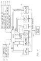
- FIG. 1 illustrates a block diagram of one embodiment of a system 100 in which a hard disk controller (HDC) 122 is typically used.
- An HDC core 102 is connected via a host bus interface 110 to a host system 108 using a host system bus 112.
- the host system 108 may consist of one or more host system microprocessors, system RAM, a monitor, a keyboard, and other devices.
- the host system 108 exchanges data to be stored on or retrieved from a hard disk 114 through the host system bus 112. Instructions from the host system 108 to the HDC core 102 regarding, for example, what data to retrieve or where to store data are also sent over the host system bus 112.
- a controller microprocessor 104 is connected to the HDC core 102 through a microprocessor interface 106.
- the controller microprocessor 104 which, in one embodiment, is distinct from the host system microprocessor, receives and executes instructions from the host system 108 and manages the HDC core 102.
- the hard disk 114 is connected to the HDC core 102 through a disk formatter 116. As discussed in greater detail below, the disk formatter 116 controls the operation of the hard disk 114. In the illustrated embodiment, the hard disk 114 consists of a magnetic disk device and associated circuitry.
- a controller buffer memory 118 is connected to the HDC core 102 through a buffer interface 120. In one embodiment, the buffer memory 118 is configured using random access memory (RAM).
- RAM may be dynamic or static.
- FIG. 2 illustrates one embodiment of the HDC core 102 and associated ports 204, 208, 210, 216.
- the bus interface 202 sends and receives information from the host system 108 through data, control, and interrupt lines of the host bus port 204.
- the microprocessor interface logic 206 connects the controller microprocessor 104 to the HDC core 102 through timing, address, and data lines of the controller microprocessor port 208.
- the microprocessor bus 220 allows the controller microprocessor 104 to communicate with and control the various units in the HDC 102 core.
- the disk formatter 116 is connected to the disk 114 through the data and control lines of the disk port 210.
- a Reed Soloman error correction code (ECC) engine 212 is connected to the disk formatter 116 via a bus.
- the ECC engine 212 performs error correction on disk reads, as well as error correction code generation on disk writes.
- a buffer controller 214 is connected to the buffer memory 118 through the address, timing, and data lines of the buffer port 216.
- the buffer controller 214 includes an arbiter (not shown) which controls access to the buffer memory 118 by the disk formatter 116, the ECC engine 212, the host bus interface 202, and the microprocessor interface 206, in addition to other units discussed below.
- the arbiter is later discussed in greater detail.
- the various units that access the buffer memory 118 do so through the data bus 218.
- the data bus 218 is coupled to the buffer memory 118 via the buffer port 216.
- Figure 3 depicts one embodiment of the HDC's bus architecture.
- the units which access the buffer memory 118 do so through respective "first in first out” (FIFO) buffers 308, 312, 314, 316, 318 and 320.
- FIFO buffers may vary in size. In one embodiment, the FIFO buffers each have between 64 to 96 bytes of storage.
- the controller microprocessor 104 accesses the buffer memory 118 through the microprocessor FIFO 308.
- the buffer memory 118 serves as the main memory, storing instructions and data, for the controller microprocessor 104.
- a disk format data fetch unit 304 operates to fetch disk format data from the buffer memory 118.
- the disk formatter 116 uses this data to locate and organize host system data on the hard disk 114.
- the memory refresh unit 306 operates to refresh the buffer memory 118 at required intervals when the buffer memory uses dynamic RAM.
- both the disk format data fetch unit 304 and the memory refresh unit 306 share one arbitration slot for the purposes of buffer memory access arbitration.
- only one of the disk format data fetch unit 304 and the memory refresh unit 306 may access the buffer memory 118 in a single access cycle.
- the memory refresh unit 306 and disk format data fetch unit 304 may each have their own arbitration slot.
- the disk format data fetch unit 304 and the memory refresh unit 306 access the buffer memory 118 through their respective FIFO buffers 314 and 316.
- the ECC engine 212 is connected to the buffer memory 118 through a FIFO 318.
- the ECC engine FIFO 318 is used to correct data read from the hard disk 114 while the data is in the buffer memory 118.
- the buffer controller 214 effectuates the correction through a read/modify/write process.
- the host bus interface 110 is connected to the buffer memory 118 through its FIFO 320.
- the host bus interface 110 channels data and instructions between the host system 108 and the buffer memory 118.
- Figure 4 illustrates one embodiment of the connectivity between the disk formatter 116, the disk format data fetch unit 304, the memory refresh unit 306, the ECC engine 212, the microprocessor FIFO 308, the host bus interface 110 and an arbiter 402.
- the arbiter 402 arbitrates between the various units accessing the buffer memory.
- the arbiter 402 grants access to requesting units during a repeating access cycle.
- An access cycle is a period of time during which access is offered to each unit, or a group of units sharing an access slot, that access the buffer memory.
- each unit has a request line, titled "REQ,” for requesting access to the buffer memory 118. as well as an acknowledge line, titled "ACK,” by way of which the arbiter 402 grants a requested access.
- the arbitration limit registers include: the disk formatter arbitration limit register 410, the shared disk format data fetch unit and memory refresh unit arbitration limit register 412, the ECC engine arbitration limit register 414, the microprocessor FIFO arbitration limit register 416, and the host bus interface (global) arbitration limit register 418. Note that the disk format data fetch unit 306 and the memory refresh unit 306 share the same arbitration limit and use the same arbitration limit register 412.
- the host bus interface arbitration limit register 418 is also called the global arbitration limit register for reasons that will be discussed below.
- the arbitration limit registers 410-418 store time limits defined in HDC clock cycles for each unit's maximum specified access duration during an access cycle. In one embodiment, the access duration is for a continuous time period.
- an arbitration limit counter 406 and a global arbitration limit counter 408, also connected to the arbiter 402 are an arbitration limit counter 406 and a global arbitration limit counter 408, used to keep track of the access durations of the units by loading and decrementing arbitration limit values.
- the global arbitration limit counter 408 tracks the available access time of the host bus interface and the arbitration limit counter 406 tracks the available access time for the remaining units.
- Figure 5 illustrates an exemplary disk write sequence 500 as the write data passes through various units of the HDC 102.
- Data 502 from the host system 108 arrives at the host bus interface 110 and is passed through the host bus interface FIFO 320 to the buffer memory 118.
- the FIFO 320 buffers the data 502 as needed while waiting for access to the buffer memory 118.
- data is read from or stored on the disk 114 in units no smaller than a sector, which is typically 512 bytes. If a quantity of data less than a sector needs to be accessed, a whole sector is nevertheless accessed.
- the data 502 is then directed to the disk formatter 116 via the disk formatter FIFO 312 along with a cyclic redundancy check (CRC) tag.
- CRC cyclic redundancy check
- the CRC is a code generated from the data that can be used to confirm the correctness of the data.
- the FIFO 312 buffers the data 502 as it arrives from the buffer memory 118. While the data 502 and CRC 508 are en route to the disk formatter 116, the data 502 and CRC 508 are also passed through the ECC engine 212, which generates an error correction code (ECC) 510.
- ECC error correction code
- the ECC 510 is passed to the disk formatter 116 to be appended to the data 502 and the CRC 508, all of which is then written to the hard disk 114 by the disk formatter 116.
- Figure 6 illustrates an exemplary disk read sequence 600 as the data passes through the units of the HDC 102.
- ECC techniques are used to compensate for the possibility that a sector's data 604, CRC 606 and ECC 602 might become corrupted during the process of being written and read from the hard disk 114.
- the ECC engine 212 performs the task of correcting the uncorrected data 604 and/or CRC 606 after it has been retrieved from the hard disk 114.
- the disk formatter 116 sends the uncorrected data 604, CRC 606 and ECC 602 to the ECC engine 212.
- the disk formatter 116 also strips off the ECC 602 and passes the uncorrected data 604 and CRC 606 to the disk formatter FIFO 312 and then on to the buffer memory 118.
- the disk formatter FIFO 312 absorbs any latency when waiting to access the buffer memory 118. While the uncorrected data 604 and CRC 606 are stored in the buffer memory 118, the ECC engine 212 executes an algorithm that creates error correction information 612 from the uncorrected data 604, CRC 600, and ECC 602. The ECC engine 212 passes this error correction information 612 on to the ECC FIFO 318.
- the buffer controller 214 uses the error correction information 612 in the ECC FIFO 318 to attempt to correct any errors in the uncorrected data 604 and the CRC 606 residing in the buffer memory 118.
- the buffer controller 214 corrects the data 604 and the CRC 606 by reading the uncorrected data 604 and/or CRC 606 from the buffer memory 118, appropriately modifying the uncorrected data 604 and/or CRC 606 using the information 614 in the ECC FIFO 318 and then writing the corrected data 616 and/or CRC 618 back to the buffer memory 118.
- the corrected data 616 and CRC 618 are then passed to the host bus interface FIFO 320.
- the CRC 618 is then checked.
- the CRC check determines whether the data correction operation was successful. If the data 616 is correct, the data 616 is passed to the host bus interface 110 and on to the host system 108. If the data 616 is not correct, an error signal is generated and directed to the host system.
- the controller microprocessor 104 accesses the buffer memory 118 since the buffer memory serves as the microprocessor's main memory. Furthermore, upon performing a disk write or read, the disk formatter 116 utilizes disk format information retrieved by the disk format data fetch unit 304 and stored in the buffer memory 118. The buffer memory's dynamic RAM 118 also needs to be refreshed periodically and thus the buffer memory refresh unit 306 accesses the buffer memory as well.
- the arbiter 402 functions through the use of settable arbitration limits.
- the arbitration limits correspond to the numbers of clock cycles representing the maximum access time for a corresponding unit.
- the limits may be programmed in non-volatile memory such as ROM or EEPROM. Alternatively, the arbitration limits may be determined and set on the fly by the host system or the controller microprocessor.
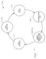
- Figure 7 illustrates one embodiment of an access cycle 700.
- the arbiter 402 checks each unit for access requests in a predetermined, repeating order. If a unit has not raised its REO line to the arbiter 402, the arbiter 402 then checks the next unit's REO line. The arbiter 402 continues around the access cycle until it finds a unit requesting buffer memory access. Note that memory refresh unit 306 and disk format data fetch unit 304 compete for the same access cycle slot. In a given access cycle, the arbiter may only grant access to one of the memory refresh unit 306 or the disk format data fetch unit 304.
- the arbiter 402 gives priority to the memory refresh unit 306 as the buffer memory needs to be refreshed to avoid losing its contents; the disk format data fetch unit 304 then waits until the next access cycle to gain access.
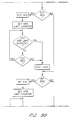
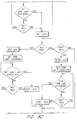
- FIG 8 shows a detailed flowchart 800 of one embodiment of a single access cycle of the arbitration process.
- the arbitration process is controlled using an arbiter state machine. Because the arbitration process runs in a cycle, the choice of a start location is not critical. For the purposes of illustration, however, a start state 802 is shown.
- the first portion of the arbitration process 804-814 is directed to disk formatter access.
- the arbiter 402 checks whether the disk formatter 116 is requesting buffer memory access by checking the disk formatter REQ line. If the disk formatter 116 is requesting access, the arbiter 402 grants access, at state 806, by raising the disk formatter's ACK line.
- the arbiter 402 reads the disk formatter arbitration limit from the corresponding arbitration limit register 410 and loads the limit into the arbitration limit counter 406.
- the arbitration limit counter 406 is decremented (counts down by one) during each HDC clock cycle.
- the arbiter 402 repeatedly checks whether the arbitration limit counter 406 has reached zero and whether the disk formatter's request line REG is still active. If the arbitration limit counter 406 has reached zero or if the disk formatter's request line REG is inactive, at stage 814 the arbiter 402 deasserts the disk formatter's acknowledge ACK line. If, at state 804 mentioned above, the disk formatter 116 is not requesting access, the arbiter proceeds directly from state 804 to state 816.
- the arbiter 402 loads the global arbitration limit from the global arbitration limit register 418 into the global arbitration limit counter 408.
- the global arbitration limit counter 408 is decremented during each clock cycle of the remainder of the access cycle.
- the global arbitration limit is decremented while the ECC engine 212, the microprocessor FIFO 308, the disk format data fetch/memory refresh units 304/306 and the bus interface unit 110 are accessing the buffer memory 118.
- the global arbitration limit counter 408 reaches zero, a new access cycle begins and access is again offered to the disk formatter 116.
- the global arbitration limit serves two purposes. First, the global arbitration limit limits the time available to all units other than the disk formatter 116. Second, the global arbitration limit serves, in effect, as the arbitration limit for the host interface unit 110.
- Each of the ECC engine 212, the microprocessor FIFO 308, and the disk format data fetch/memory refresh units 3041306 has its own arbitration limit. While each of these units are accessing the buffer memory 118, the arbitration limit counter 406 counts down from the corresponding arbitration limits. Further, while each of these units are accessing the buffer memory 118, the global arbitration limit counter 408 counts down from the global arbitration limit to determine the time that will eventually be offered to the host interface unit 110. Once the ECC engine 212, the microprocessor FIFO 308, and the disk format data fetch/memory refresh units 304/306 have completed their accesses, the host interface unit 110 is given access for the time remaining in the global arbitration limit counter 408.
- the arbiter 402 proceeds to state 818 to determine if the ECC engine 212 is requesting access by checking the ECC engine REQ line. If the ECC engine 212 is requesting access, the arbiter proceeds to state 820 and grants access by asserting the ECC engine's ACK line. At this point, the arbiter 402 reads the ECC engine arbitration limit from the corresponding arbitration limit register 412, and proceeding to state 822, sets the arbitration limit counter 406. The arbitration limit counter 406 is decremented each clock cycle during the ECC engine access time period. Note that the global arbitration limit counter 408 is also decremented during this time. Next, the arbiter 402 at states 824.
- the arbiter 402 proceeds to offer access to the microprocessor FIFO 308 at states 830-840 in a manner similar to that described above with respect to the ECC engine access. As with the ECC engine 212, while access is granted to the microprocessor FIFO 308, both the arbitration limit counter 406 and global arbitration limit counter 408 are decremented each clock cycle. Once the arbiter 402 has completed the microprocessor FIFO portion of the access cycle, the arbiter 402 proceeds to state 842.
- the arbiter 402 grants access to only one of the memory refresh unit 306 and the disk format data fetch unit 304 in a single access cycle.
- the flowchart branches at state 842 to accommodate this feature.
- a buffer memory refresh unit request takes priority over a disk format data fetch unit request. Therefore, the arbiter 402 first determines whether the refresh unit 306 is requesting access. If the refresh unit 306 is requesting access, the arbiter 402 follows a sequence 844-852 similar to those described above for the previous units. Of course, in this case the arbitration limit counter 406 is loaded with the refresh/data fetch arbitration limit.
- the arbiter 402 proceeds to state 854 and determines whether the disk format data fetch unit 304 is requesting access. If so, then the arbiter 402 follows a sequence 856-864 similar to the sequence for the refresh unit 306. If neither the disk format data fetch unit 304 nor the refresh unit 306 request access, the arbiter 402 proceeds directly from state 854 to state 866. At this point the arbiter 402 offers access to the host interface 110.
- the access duration of the host interface 110 is limited only by the global arbitration limit.
- the global arbitration limit counter 406 is reset after access is offered to the disk formatter 116 and before access is offered to the ECC engine 212 and is then continually decremented while the units previous to the host interface 110 access the buffer memory 118.
- the host interface 110 is allowed access for the remainder of the global arbitration limit not used by the previous units. Note that the amount of time during which the disk formatter 116 accesses the buffer memory 28 does not affect the global arbitration limit counter 408 or the amount of time allocated to the host interface 110. This is because the global arbitration limit counter 408 is set only after the disk formatter 116 has had its turn during the access cycle.
- the host interface is flexibly offered an access time ranging from a predetermined minimum to a maximum as large as the global arbitration limit in a continuous block of time.
- the arbiter To allocate access to the host interface 110, at state 866, the arbiter first checks whether the host interface 110 is requesting access. If so, at state 868, the arbiter asserts host interface ACK line, thereby granting access to the buffer memory 118.
- the global arbitration limit counter 408 continues to be decremented while the host interface unit 110 is granted access. In the present embodiment, the global arbitration limit is sufficiently large to accommodate the arbitration limits of the previous units and still have at least some remaining time for the host interface unit.
- the arbiter 402 repeatedly checks to see whether the global arbitration limit counter 408 has reached zero and whether the host interface unit 110 is still requesting access.
- the arbiter 402 deasserts the host interface's ACK line. If, at state 866, the host interface 110 is not requesting access, the arbiter 402 proceeds from state 866 to state 876. At this point the arbiter 402 has completed one access cycle and returns to the start state 802 of the flowchart 800.
- Figure 9 shows several exemplary arbitration limits and associated timing diagrams illustrating the arbiter operation.
- an arbitration limit denotes the number of HDC clock cycles of each access cycle available to a corresponding unit during which the unit can access the buffer memory 118.
- time lines 902-918 time begins towards the left side of the figure.
- the first time line 902 illustrates that at a top level, the arbitration process can be divided into two parts. The first part consists of the time allocated to the disk formatter 116, the disk arbitration limit. The second part consists of the time allocated to all of the other units, the global arbitration limit.
- the second time line 904 illustrates that the time available to the host interface 110, represented by the dynamic host interface arbitration limit, is the time represented by the global arbitration limit, diminished by the time granted to the ECC 212, microprocessor 308, refresh/data fetch 3041306 units.
- Time line 906 illustrates that in one embodiment, the combined ECC arbitration limit, the microprocessor arbitration limit, and the refresh/format data fetch arbitration limits are less than the global arbitration limit, thereby ensuring a minimum amount of time, the minimum host interface arbitration limit, is allocated to the host interface unit 110.
- the ECC 212, microprocessor 308 and the refresh/data fetch 304/306 units use all of their available access time, there will still be time remaining for the host interface 110 to access the buffer memory 118.
- Figure 9 illustrates timing diagrams for exemplary buffer memory arbitration sequences 908-918: In each diagram, one complete access cycle is shown, illustrating how the access cycle time can vary.
- the first exemplary arbitration sequence 908 shows the relative access time allocated to each unit when all units are requesting their maximum access time. In this case, the total access cycle time is at its maximum.
- the ECC engine 212 deasserts its REQ line and ceases access about halfway through the allocated arbitration time shown in 906.
- the microprocessor FIFO 308 does not request access at all, but the host interface 110 requests, and is granted all of the remaining available time.
- the ECC engine 212, refresh/data fetch units 304/306 and microprocessor 308 do not request buffer access.
- the complete global arbitration limit is made available to the host interface 110.
- both the disk formatter 116 and the host interface 110 use all of the time available to each.
- the disk formatter 116 releases its REQ line and only uses about half of its available time.
- the ECC engine 212, refresh/data fetch units 304/306, and the host interface 110 use all of their available access time. Because the disk formatter 116 relinquishes its access early, the complete access cycle time is less than in the previous sequences.
- the sequence 916 is similar to the sequence 914, except that the ECC 212, microprocessor 308 and refresh/data fetch 304/306 units do not request access. However, the host interface 110 requests maximum access in this case and uses the time given up by the other units.
- the last sequence 918 depicts a situation where the disk formatter 116 requests its full access time, the ECC 212, microprocessor 308 or refresh/data fetch 304/306 units do not request access, and the host interface 110 only requests a fraction of its available access time. In this case, because the global arbitration limit is never reached, the total access cycle time is substantially less than the maximum possible access cycle time.
- Arbitration limits may be based on several factors including the following: the disk formatter FIFO size, the width of the buffer memory data bus, the hard disk data read/write rate, the clock speed of the HDC 102, the time delay before requested data is read from the buffer memory 118 and the time it takes for the arbiter 402 to perform its operations, among others. These factors are typically constant and can be determined at the time of design and manufacture of the hard disk unit.
- the arbitration limits can be stored in non-volatile memory, or alternatively, these factors can be determined dynamically, during system operation.
- the global arbitration limit is set to optimize the utilization of the hard disk 114. This is accomplished by ensuring that the disk formatter FIFO 312 is never left empty or full.
- the global arbitration limit defines the number of clock cycles between the time the disk formatter 116 gives up access to the buffer memory 118 on a previous cycle and the time that data again arrives at the FIFO 312 from the buffer memory 118 on a subsequent cycle. As long as there is data in the FIFO 312 on a disk write and as long as the FIFO 312 is not full on a disk read, the hard disk 114 will be optimally utilized.
- data 502 is transferred from the buffer memory 118 to the disk formatter FIFO 312.
- the disk formatter FIFO 312 is continually emptied, with data being written to the hard disk 114 at the disk data rate.
- the disk data rate is the rate at which data can be written to or read from the hard disk 114.
- the time it takes to empty a full disk formatter FIFO 312 can thus be defined as: Time to empty - FIFO size / disk data rate This time can be multiplied by the clock frequency to yield the time in clock cycles.
- the arbiter 402 takes a finite number of clock cycles, called the arbitration delay, in order to grant access to a unit.
- the setup time in order to set up the buffer memory 118 to begin transferring data.
- the read delay in order to transfer data from the buffer memory 118 to the disk formatter FIFO 312.
- the fact that the disk formatter FIFO 312 is being both emptied and filled simultaneously needs to be taken into consideration.
- the disk formatter 116 has access to and is transferring data from the buffer memory 118 to the disk formatter FIFO 312, the disk formatter 116 is simultaneously emptying the FIFO 312 to the hard disk 114.
- the net rate at which it is being filled is the difference in the rates at which data is being placed in the FIFO 312 and at which data is being removed from the FIFO 312.
- the rate at which the data is placed in the FIFO 312, called the buffer data rate, is equal to the HDC's bus width times the clock frequency.
- the disk formatter FIFO size is divided by the fill rate to determine the time to fill the disk formatter FIFO 312. This result is multiplied by the clock frequency to yield the number of clock cycles to fill the disk formatter FIFO 312:
- Clock cycles to fill ( FIFO size ) * clock frequency / ( ( bus width ) * clock frequency - disk data rate )
- the disk formatter 116 and hard disk 114 achieve optimal utilization.
- the arbitration limits of the other units within the HDC 102 are constrained by the global arbitration limit.
- the memory refresh/disk format data fetch units 3041306 and the ECC engine 212 typically have predictable buffer utilization characteristics. Thus, arbitration limits can be easily selected in accordance with those characteristics.
- the microprocessor FIFO's arbitration limit accommodates a reasonable expectation of usage.
- the host bus interface usage is fairly unpredictable so the bus interface unit 110 is allocated the remaining access time.
- two or more units are allocated access time outside the scope of the global arbitration limit.
- no units are allocated access time outside the scope of the global arbitration limit. Rather, all of the units are granted access within the global arbitration limit and thus the global arbitration limit alone defines the maximum access cycle time.
- the number of units limited under the global arbitration limit can be varied.
- additional global arbitration limits can be added that operate concurrently or sequentially.
- Other embodiments are contemplated in which additional units may access the buffer memory 118 in a manner similar to the disk formatter 116, outside of the global arbitration limit.
Landscapes
- Engineering & Computer Science (AREA)
- Theoretical Computer Science (AREA)
- Human Computer Interaction (AREA)
- Physics & Mathematics (AREA)
- General Engineering & Computer Science (AREA)
- General Physics & Mathematics (AREA)
- Bus Control (AREA)
- Signal Processing For Digital Recording And Reproducing (AREA)
- Information Transfer Systems (AREA)
- Memory System Of A Hierarchy Structure (AREA)
- Multi Processors (AREA)
- Techniques For Improving Reliability Of Storages (AREA)
- Storage Device Security (AREA)
Applications Claiming Priority (3)
| Application Number | Priority Date | Filing Date | Title |
|---|---|---|---|
| US275629 | 1999-03-24 | ||
| US09/275,629 US6530000B1 (en) | 1999-03-24 | 1999-03-24 | Methods and systems for arbitrating access to a disk controller buffer memory by allocating various amounts of times to different accessing units |
| PCT/US2000/007780 WO2000057267A1 (en) | 1999-03-24 | 2000-03-23 | Arbitration methods and systems for arbitrating access to a disk controller memory |
Publications (2)
| Publication Number | Publication Date |
|---|---|
| EP1163573A1 EP1163573A1 (en) | 2001-12-19 |
| EP1163573B1 true EP1163573B1 (en) | 2007-08-01 |
Family
ID=23053180
Family Applications (1)
| Application Number | Title | Priority Date | Filing Date |
|---|---|---|---|
| EP00918322A Expired - Lifetime EP1163573B1 (en) | 1999-03-24 | 2000-03-23 | Arbitration methods and systems for arbitrating access to a disk controller memory |
Country Status (9)
| Country | Link |
|---|---|
| US (1) | US6530000B1 (enExample) |
| EP (1) | EP1163573B1 (enExample) |
| JP (1) | JP4313516B2 (enExample) |
| KR (1) | KR100619806B1 (enExample) |
| AT (1) | ATE368885T1 (enExample) |
| AU (1) | AU3915300A (enExample) |
| CA (1) | CA2364625C (enExample) |
| DE (1) | DE60035774T2 (enExample) |
| WO (1) | WO2000057267A1 (enExample) |
Families Citing this family (32)
| Publication number | Priority date | Publication date | Assignee | Title |
|---|---|---|---|---|
| US6715009B1 (en) * | 1999-12-21 | 2004-03-30 | Intel Corporation | Method and apparatus for coordinating cooperating resources and its application |
| US7406547B2 (en) * | 2000-08-09 | 2008-07-29 | Seagate Technology Llc | Sequential vectored buffer management |
| US6763437B1 (en) * | 2000-09-07 | 2004-07-13 | Maxtor Corporation | Control system, storage device and method for controlling access to a shared memory using a bus control or handshaking protocol |
| JP4213338B2 (ja) * | 2000-12-22 | 2009-01-21 | 富士通マイクロエレクトロニクス株式会社 | リアルタイムレコーディングシステム及びリアルタイムレコーディング方法 |
| US7111228B1 (en) | 2002-05-07 | 2006-09-19 | Marvell International Ltd. | System and method for performing parity checks in disk storage system |
| US7007114B1 (en) * | 2003-01-31 | 2006-02-28 | Qlogic Corporation | System and method for padding data blocks and/or removing padding from data blocks in storage controllers |
| US7287102B1 (en) | 2003-01-31 | 2007-10-23 | Marvell International Ltd. | System and method for concatenating data |
| US7099963B2 (en) * | 2003-03-10 | 2006-08-29 | Qlogic Corporation | Method and system for monitoring embedded disk controller components |
| US7492545B1 (en) | 2003-03-10 | 2009-02-17 | Marvell International Ltd. | Method and system for automatic time base adjustment for disk drive servo controllers |
| US7219182B2 (en) * | 2003-03-10 | 2007-05-15 | Marvell International Ltd. | Method and system for using an external bus controller in embedded disk controllers |
| US7039771B1 (en) | 2003-03-10 | 2006-05-02 | Marvell International Ltd. | Method and system for supporting multiple external serial port devices using a serial port controller in embedded disk controllers |
| US7064915B1 (en) | 2003-03-10 | 2006-06-20 | Marvell International Ltd. | Method and system for collecting servo field data from programmable devices in embedded disk controllers |
| US7870346B2 (en) * | 2003-03-10 | 2011-01-11 | Marvell International Ltd. | Servo controller interface module for embedded disk controllers |
| US7526691B1 (en) | 2003-10-15 | 2009-04-28 | Marvell International Ltd. | System and method for using TAP controllers |
| US7206922B1 (en) * | 2003-12-30 | 2007-04-17 | Cisco Systems, Inc. | Instruction memory hierarchy for an embedded processor |
| US7139150B2 (en) * | 2004-02-10 | 2006-11-21 | Marvell International Ltd. | Method and system for head position control in embedded disk drive controllers |
| US7120084B2 (en) * | 2004-06-14 | 2006-10-10 | Marvell International Ltd. | Integrated memory controller |
| US8166217B2 (en) * | 2004-06-28 | 2012-04-24 | Marvell International Ltd. | System and method for reading and writing data using storage controllers |
| US7757009B2 (en) * | 2004-07-19 | 2010-07-13 | Marvell International Ltd. | Storage controllers with dynamic WWN storage modules and methods for managing data and connections between a host and a storage device |
| US9201599B2 (en) * | 2004-07-19 | 2015-12-01 | Marvell International Ltd. | System and method for transmitting data in storage controllers |
| US8032674B2 (en) * | 2004-07-19 | 2011-10-04 | Marvell International Ltd. | System and method for controlling buffer memory overflow and underflow conditions in storage controllers |
| US7386661B2 (en) | 2004-10-13 | 2008-06-10 | Marvell International Ltd. | Power save module for storage controllers |
| US7240267B2 (en) | 2004-11-08 | 2007-07-03 | Marvell International Ltd. | System and method for conducting BIST operations |
| US7802026B2 (en) * | 2004-11-15 | 2010-09-21 | Marvell International Ltd. | Method and system for processing frames in storage controllers |
| US7609468B2 (en) | 2005-04-06 | 2009-10-27 | Marvell International Ltd. | Method and system for read gate timing control for storage controllers |
| JP2006301810A (ja) * | 2005-04-18 | 2006-11-02 | Fujitsu Ltd | データ転送処理方法、データ転送処理装置およびデータ転送処理制御プログラム |
| US8108659B1 (en) * | 2006-11-03 | 2012-01-31 | Nvidia Corporation | Controlling access to memory resources shared among parallel synchronizable threads |
| JP5354816B2 (ja) * | 2008-10-15 | 2013-11-27 | マーベル ワールド トレード リミテッド | N個のデータを入出力するhdc、および、その方法 |
| CN102385555B (zh) * | 2010-08-27 | 2015-03-04 | 深圳市朗科科技股份有限公司 | 一种缓存系统和数据缓存的方法 |
| US9268649B1 (en) * | 2011-06-23 | 2016-02-23 | Western Digital Technologies, Inc. | Disk drive with recent write streams list for data refresh determination |
| US20130132621A1 (en) * | 2011-11-23 | 2013-05-23 | Ankit Sihare | Method and apparatus to share hardware resources across storage controllers within a system using resource sharing module |
| US9886209B2 (en) * | 2016-02-16 | 2018-02-06 | Lenovo Enterprise Solutions (Singapore) Pte. Ltd. | Controlling file placement on a disk drive to improve file access |
Family Cites Families (28)
| Publication number | Priority date | Publication date | Assignee | Title |
|---|---|---|---|---|
| US4000485A (en) | 1975-06-30 | 1976-12-28 | Honeywell Information Systems, Inc. | Data processing system providing locked operation of shared resources |
| US4558429A (en) | 1981-12-17 | 1985-12-10 | Honeywell Information Systems Inc. | Pause apparatus for a memory controller with interleaved queuing apparatus |
| US5276807A (en) | 1987-04-13 | 1994-01-04 | Emulex Corporation | Bus interface synchronization circuitry for reducing time between successive data transmission in a system using an asynchronous handshaking |
| US5193197A (en) | 1987-09-24 | 1993-03-09 | Digital Equipment Corporation | Apparatus and method for distributed dynamic priority arbitration for access to a shared resource |
| US5072420A (en) | 1989-03-16 | 1991-12-10 | Western Digital Corporation | FIFO control architecture and method for buffer memory access arbitration |
| US5506989A (en) | 1990-01-31 | 1996-04-09 | Ibm Corporation | Arbitration system limiting high priority successive grants |
| US5249271A (en) | 1990-06-04 | 1993-09-28 | Emulex Corporation | Buffer memory data flow controller |
| US5301333A (en) | 1990-06-14 | 1994-04-05 | Bell Communications Research, Inc. | Tree structured variable priority arbitration implementing a round-robin scheduling policy |
| JP2703668B2 (ja) | 1991-03-18 | 1998-01-26 | 株式会社日立製作所 | データ転送制御装置および磁気ディスク制御装置 |
| DE69230462T2 (de) | 1991-11-19 | 2000-08-03 | Sun Microsystems, Inc. | Arbitrierung des Multiprozessorzugriffs zu gemeinsamen Mitteln |
| CA2080608A1 (en) | 1992-01-02 | 1993-07-03 | Nader Amini | Bus control logic for computer system having dual bus architecture |
| US5408644A (en) | 1992-06-05 | 1995-04-18 | Compaq Computer Corporation | Method and apparatus for improving the performance of partial stripe operations in a disk array subsystem |
| US5524268A (en) | 1992-06-26 | 1996-06-04 | Cirrus Logic, Inc. | Flexible processor-driven control of SCSI buses utilizing tags appended to data bytes to determine SCSI-protocol phases |
| US5276662A (en) * | 1992-10-01 | 1994-01-04 | Seagate Technology, Inc. | Disc drive with improved data transfer management apparatus |
| US5546548A (en) | 1993-03-31 | 1996-08-13 | Intel Corporation | Arbiter and arbitration process for a dynamic and flexible prioritization |
| US5465343A (en) | 1993-04-30 | 1995-11-07 | Quantum Corporation | Shared memory array for data block and control program storage in disk drive |
| US5487170A (en) | 1993-12-16 | 1996-01-23 | International Business Machines Corporation | Data processing system having dynamic priority task scheduling capabilities |
| JPH07244635A (ja) | 1994-01-14 | 1995-09-19 | Fujitsu Ltd | バス使用権調停回路及び方法 |
| US5574867A (en) | 1994-07-08 | 1996-11-12 | Intel Corporation | Fast first-come first served arbitration method |
| US5519837A (en) | 1994-07-29 | 1996-05-21 | International Business Machines Corporation | Pseudo-round-robin arbitration for a shared resource system providing fairness and high throughput |
| US5881313A (en) | 1994-11-07 | 1999-03-09 | Digital Equipment Corporation | Arbitration system based on requester class and relative priority including transmit descriptor valid bit for a shared resource having multiple requesters |
| US5546545A (en) | 1994-12-09 | 1996-08-13 | International Business Machines Corporation | Rotating priority selection logic circuit |
| US5623672A (en) | 1994-12-23 | 1997-04-22 | Cirrus Logic, Inc. | Arrangement and method of arbitration for a resource with shared user request signals and dynamic priority assignment |
| WO1996035173A1 (en) | 1995-05-03 | 1996-11-07 | Apple Computer, Inc. | Arbitration of computer resource access requests |
| US5664121A (en) | 1995-11-07 | 1997-09-02 | Sun Microsystems, Inc. | Dual mode arbitration apparatus and method for reducing latency by allowing the possibility of simultaneous request and access for a shared bus |
| US5692135A (en) | 1995-12-14 | 1997-11-25 | International Business Machines Corporation | Method and system for performing an asymmetric bus arbitration protocol within a data processing system |
| US5784569A (en) | 1996-09-23 | 1998-07-21 | Silicon Graphics, Inc. | Guaranteed bandwidth allocation method in a computer system for input/output data transfers |
| US6178486B1 (en) * | 1998-02-19 | 2001-01-23 | Quantum Corporation | Time allocation shared memory arbitration for disk drive controller |
-
1999
- 1999-03-24 US US09/275,629 patent/US6530000B1/en not_active Expired - Lifetime
-
2000
- 2000-03-23 DE DE60035774T patent/DE60035774T2/de not_active Expired - Lifetime
- 2000-03-23 CA CA2364625A patent/CA2364625C/en not_active Expired - Lifetime
- 2000-03-23 KR KR1020017012114A patent/KR100619806B1/ko not_active Expired - Lifetime
- 2000-03-23 EP EP00918322A patent/EP1163573B1/en not_active Expired - Lifetime
- 2000-03-23 WO PCT/US2000/007780 patent/WO2000057267A1/en not_active Ceased
- 2000-03-23 AT AT00918322T patent/ATE368885T1/de not_active IP Right Cessation
- 2000-03-23 AU AU39153/00A patent/AU3915300A/en not_active Abandoned
- 2000-03-23 JP JP2000607076A patent/JP4313516B2/ja not_active Expired - Lifetime
Non-Patent Citations (1)
| Title |
|---|
| None * |
Also Published As
| Publication number | Publication date |
|---|---|
| EP1163573A1 (en) | 2001-12-19 |
| ATE368885T1 (de) | 2007-08-15 |
| JP2002540499A (ja) | 2002-11-26 |
| KR20010110679A (ko) | 2001-12-13 |
| CA2364625C (en) | 2012-08-07 |
| KR100619806B1 (ko) | 2006-09-13 |
| CA2364625A1 (en) | 2000-09-28 |
| JP4313516B2 (ja) | 2009-08-12 |
| WO2000057267A1 (en) | 2000-09-28 |
| DE60035774D1 (de) | 2007-09-13 |
| AU3915300A (en) | 2000-10-09 |
| DE60035774T2 (de) | 2007-12-06 |
| US6530000B1 (en) | 2003-03-04 |
Similar Documents
| Publication | Publication Date | Title |
|---|---|---|
| EP1163573B1 (en) | Arbitration methods and systems for arbitrating access to a disk controller memory | |
| KR102519019B1 (ko) | 액세스 효율에 기초한 메모리 요청의 순서화 | |
| US6330626B1 (en) | Systems and methods for a disk controller memory architecture | |
| US6401149B1 (en) | Methods for context switching within a disk controller | |
| US5884050A (en) | Mechanism for high bandwidth DMA transfers in a PCI environment | |
| US6393506B1 (en) | Virtual channel bus and system architecture | |
| US8310880B2 (en) | Virtual channel support in a nonvolatile memory controller | |
| US10540096B2 (en) | Method and design for dynamic management of descriptors for SGL operation | |
| KR20210021302A (ko) | 메모리 제어기에서의 리프레시 방식 | |
| JP5666722B2 (ja) | メモリ・インターフェース | |
| US10108565B2 (en) | Method for on-demand fetching of SGL pointers based buffer, traffic and command requirements | |
| US5506968A (en) | Terminating access of an agent to a shared resource when a timer, started after a low latency agent requests access, reaches a predetermined value | |
| WO1996032674A2 (en) | Semiconductor memory device for mass storage block access applications | |
| KR20090018203A (ko) | 프로세서 코어 스택 익스텐션 | |
| US20040049628A1 (en) | Multi-tasking non-volatile memory subsystem | |
| JP2024512625A (ja) | アービトレーション中の書き込みバンクグループのマスク | |
| US5301332A (en) | Method and apparatus for a dynamic, timed-loop arbitration | |
| US10929061B2 (en) | Memory system and memory control method | |
| CA2370596C (en) | Systems and methods for a disk controller memory architecture | |
| KR102334473B1 (ko) | 적응형 딥러닝 가속 장치 및 방법 | |
| US6938118B1 (en) | Controlling access to a primary memory | |
| US20050097272A1 (en) | Disk array device and control method of disk array device | |
| JP2008269176A (ja) | バスマスタ装置、情報処理システム、バスマスタ装置の制御方法並びにコンピュータプログラム | |
| JP2000090045A (ja) | データ転送システム、ダイレクトメモリアクセス制御装置及び方法、並びに記録媒体 | |
| JPH08115251A (ja) | コンピュータ・システム |
Legal Events
| Date | Code | Title | Description |
|---|---|---|---|
| PUAI | Public reference made under article 153(3) epc to a published international application that has entered the european phase |
Free format text: ORIGINAL CODE: 0009012 |
|
| 17P | Request for examination filed |
Effective date: 20011005 |
|
| AK | Designated contracting states |
Kind code of ref document: A1 Designated state(s): AT BE CH CY DE DK ES FI FR GB GR IE IT LI LU MC NL PT SE |
|
| AX | Request for extension of the european patent |
Free format text: AL;LT;LV;MK;RO;SI |
|
| 17Q | First examination report despatched |
Effective date: 20060721 |
|
| GRAP | Despatch of communication of intention to grant a patent |
Free format text: ORIGINAL CODE: EPIDOSNIGR1 |
|
| GRAS | Grant fee paid |
Free format text: ORIGINAL CODE: EPIDOSNIGR3 |
|
| GRAA | (expected) grant |
Free format text: ORIGINAL CODE: 0009210 |
|
| RAP1 | Party data changed (applicant data changed or rights of an application transferred) |
Owner name: MARVELL WORLD TRADE LTD. |
|
| AK | Designated contracting states |
Kind code of ref document: B1 Designated state(s): AT BE CH CY DE DK ES FI FR GB GR IE IT LI LU MC NL PT SE |
|
| REG | Reference to a national code |
Ref country code: GB Ref legal event code: FG4D |
|
| REG | Reference to a national code |
Ref country code: CH Ref legal event code: EP |
|
| REG | Reference to a national code |
Ref country code: IE Ref legal event code: FG4D |
|
| REF | Corresponds to: |
Ref document number: 60035774 Country of ref document: DE Date of ref document: 20070913 Kind code of ref document: P |
|
| ET | Fr: translation filed | ||
| PG25 | Lapsed in a contracting state [announced via postgrant information from national office to epo] |
Ref country code: ES Free format text: LAPSE BECAUSE OF FAILURE TO SUBMIT A TRANSLATION OF THE DESCRIPTION OR TO PAY THE FEE WITHIN THE PRESCRIBED TIME-LIMIT Effective date: 20071112 Ref country code: NL Free format text: LAPSE BECAUSE OF FAILURE TO SUBMIT A TRANSLATION OF THE DESCRIPTION OR TO PAY THE FEE WITHIN THE PRESCRIBED TIME-LIMIT Effective date: 20070801 Ref country code: FI Free format text: LAPSE BECAUSE OF FAILURE TO SUBMIT A TRANSLATION OF THE DESCRIPTION OR TO PAY THE FEE WITHIN THE PRESCRIBED TIME-LIMIT Effective date: 20070801 |
|
| NLV1 | Nl: lapsed or annulled due to failure to fulfill the requirements of art. 29p and 29m of the patents act | ||
| PG25 | Lapsed in a contracting state [announced via postgrant information from national office to epo] |
Ref country code: AT Free format text: LAPSE BECAUSE OF FAILURE TO SUBMIT A TRANSLATION OF THE DESCRIPTION OR TO PAY THE FEE WITHIN THE PRESCRIBED TIME-LIMIT Effective date: 20070801 |
|
| PG25 | Lapsed in a contracting state [announced via postgrant information from national office to epo] |
Ref country code: BE Free format text: LAPSE BECAUSE OF FAILURE TO SUBMIT A TRANSLATION OF THE DESCRIPTION OR TO PAY THE FEE WITHIN THE PRESCRIBED TIME-LIMIT Effective date: 20070801 |
|
| PG25 | Lapsed in a contracting state [announced via postgrant information from national office to epo] |
Ref country code: DK Free format text: LAPSE BECAUSE OF FAILURE TO SUBMIT A TRANSLATION OF THE DESCRIPTION OR TO PAY THE FEE WITHIN THE PRESCRIBED TIME-LIMIT Effective date: 20070801 Ref country code: GR Free format text: LAPSE BECAUSE OF FAILURE TO SUBMIT A TRANSLATION OF THE DESCRIPTION OR TO PAY THE FEE WITHIN THE PRESCRIBED TIME-LIMIT Effective date: 20071102 |
|
| PG25 | Lapsed in a contracting state [announced via postgrant information from national office to epo] |
Ref country code: PT Free format text: LAPSE BECAUSE OF FAILURE TO SUBMIT A TRANSLATION OF THE DESCRIPTION OR TO PAY THE FEE WITHIN THE PRESCRIBED TIME-LIMIT Effective date: 20080102 |
|
| PLBE | No opposition filed within time limit |
Free format text: ORIGINAL CODE: 0009261 |
|
| STAA | Information on the status of an ep patent application or granted ep patent |
Free format text: STATUS: NO OPPOSITION FILED WITHIN TIME LIMIT |
|
| PG25 | Lapsed in a contracting state [announced via postgrant information from national office to epo] |
Ref country code: SE Free format text: LAPSE BECAUSE OF FAILURE TO SUBMIT A TRANSLATION OF THE DESCRIPTION OR TO PAY THE FEE WITHIN THE PRESCRIBED TIME-LIMIT Effective date: 20071101 |
|
| 26N | No opposition filed |
Effective date: 20080506 |
|
| PG25 | Lapsed in a contracting state [announced via postgrant information from national office to epo] |
Ref country code: MC Free format text: LAPSE BECAUSE OF NON-PAYMENT OF DUE FEES Effective date: 20080331 |
|
| REG | Reference to a national code |
Ref country code: CH Ref legal event code: PL |
|
| PG25 | Lapsed in a contracting state [announced via postgrant information from national office to epo] |
Ref country code: CH Free format text: LAPSE BECAUSE OF NON-PAYMENT OF DUE FEES Effective date: 20080331 Ref country code: LI Free format text: LAPSE BECAUSE OF NON-PAYMENT OF DUE FEES Effective date: 20080331 Ref country code: IE Free format text: LAPSE BECAUSE OF NON-PAYMENT OF DUE FEES Effective date: 20080324 |
|
| PG25 | Lapsed in a contracting state [announced via postgrant information from national office to epo] |
Ref country code: CY Free format text: LAPSE BECAUSE OF FAILURE TO SUBMIT A TRANSLATION OF THE DESCRIPTION OR TO PAY THE FEE WITHIN THE PRESCRIBED TIME-LIMIT Effective date: 20070801 |
|
| PG25 | Lapsed in a contracting state [announced via postgrant information from national office to epo] |
Ref country code: LU Free format text: LAPSE BECAUSE OF NON-PAYMENT OF DUE FEES Effective date: 20080323 |
|
| PG25 | Lapsed in a contracting state [announced via postgrant information from national office to epo] |
Ref country code: IT Free format text: LAPSE BECAUSE OF NON-PAYMENT OF DUE FEES Effective date: 20080331 |
|
| REG | Reference to a national code |
Ref country code: FR Ref legal event code: PLFP Year of fee payment: 17 |
|
| REG | Reference to a national code |
Ref country code: FR Ref legal event code: PLFP Year of fee payment: 18 |
|
| REG | Reference to a national code |
Ref country code: FR Ref legal event code: PLFP Year of fee payment: 19 |
|
| PGFP | Annual fee paid to national office [announced via postgrant information from national office to epo] |
Ref country code: GB Payment date: 20190327 Year of fee payment: 20 Ref country code: FR Payment date: 20190328 Year of fee payment: 20 |
|
| PGFP | Annual fee paid to national office [announced via postgrant information from national office to epo] |
Ref country code: DE Payment date: 20190528 Year of fee payment: 20 |
|
| REG | Reference to a national code |
Ref country code: DE Ref legal event code: R071 Ref document number: 60035774 Country of ref document: DE |
|
| REG | Reference to a national code |
Ref country code: GB Ref legal event code: PE20 Expiry date: 20200322 |
|
| PG25 | Lapsed in a contracting state [announced via postgrant information from national office to epo] |
Ref country code: GB Free format text: LAPSE BECAUSE OF EXPIRATION OF PROTECTION Effective date: 20200322 |