EP1157394B1 - Anordnung zum schreiben von magnetischen massstäben - Google Patents
Anordnung zum schreiben von magnetischen massstäben Download PDFInfo
- Publication number
- EP1157394B1 EP1157394B1 EP00920470A EP00920470A EP1157394B1 EP 1157394 B1 EP1157394 B1 EP 1157394B1 EP 00920470 A EP00920470 A EP 00920470A EP 00920470 A EP00920470 A EP 00920470A EP 1157394 B1 EP1157394 B1 EP 1157394B1
- Authority
- EP
- European Patent Office
- Prior art keywords
- conductor
- shaped conductor
- section
- cross
- current
- Prior art date
- Legal status (The legal status is an assumption and is not a legal conclusion. Google has not performed a legal analysis and makes no representation as to the accuracy of the status listed.)
- Expired - Lifetime
Links
- 239000004020 conductor Substances 0.000 claims abstract description 107
- 239000003990 capacitor Substances 0.000 claims abstract description 19
- 230000000737 periodic effect Effects 0.000 claims description 3
- 238000005259 measurement Methods 0.000 claims description 2
- 239000000470 constituent Substances 0.000 claims 1
- 238000001208 nuclear magnetic resonance pulse sequence Methods 0.000 claims 1
- 238000012216 screening Methods 0.000 claims 1
- 239000007787 solid Substances 0.000 claims 1
- 230000005415 magnetization Effects 0.000 description 32
- 239000000463 material Substances 0.000 description 12
- 238000000034 method Methods 0.000 description 9
- 230000008859 change Effects 0.000 description 5
- 230000008901 benefit Effects 0.000 description 4
- 230000007423 decrease Effects 0.000 description 4
- 230000008569 process Effects 0.000 description 4
- 239000002131 composite material Substances 0.000 description 3
- 239000000696 magnetic material Substances 0.000 description 3
- 241000669069 Chrysomphalus aonidum Species 0.000 description 2
- 230000005672 electromagnetic field Effects 0.000 description 2
- 239000002184 metal Substances 0.000 description 2
- 238000010276 construction Methods 0.000 description 1
- 230000006378 damage Effects 0.000 description 1
- 230000003247 decreasing effect Effects 0.000 description 1
- 230000001419 dependent effect Effects 0.000 description 1
- 230000036541 health Effects 0.000 description 1
- 230000006872 improvement Effects 0.000 description 1
- 238000004519 manufacturing process Methods 0.000 description 1
- 230000008092 positive effect Effects 0.000 description 1
- 229910000859 α-Fe Inorganic materials 0.000 description 1
Images



Classifications
-
- H—ELECTRICITY
- H01—ELECTRIC ELEMENTS
- H01F—MAGNETS; INDUCTANCES; TRANSFORMERS; SELECTION OF MATERIALS FOR THEIR MAGNETIC PROPERTIES
- H01F13/00—Apparatus or processes for magnetising or demagnetising
- H01F13/003—Methods and devices for magnetising permanent magnets
Definitions
- the present invention relates to an arrangement for what is referred to as writing, in time Sequential section-by-section magnetization of magnetic scales.
- Magnetic scales are required for length, angle and position determination. They can be done with divisions that exist periodically or in sections magnetized in the opposite direction according to different codes his.
- Magnetic scales can be linear or circular or any have other shapes. They can be made entirely of hard magnetic material or of hard magnetic material, which is based on a soft magnetic or non-magnetic Carrier located. The surface can be protected by a cover layer.
- Arrangements for writing magnetic scales according to two different principles are known.
- the first principle e.g. published patent application DE 41 08 923 A1
- a disadvantage of this method of Magnetization of magnetic scales is that at the position of the parts of the molded extremely high accuracy requirements must be placed on the electrical conductor go beyond the accuracy requirements of the magnetic scale, because the Transfer of the intended magnetic pattern is not possible without errors.
- the Shaped electrical conductor is the product of a mechanical manufacture, so that position errors of the scale thus produced cannot be achieved in the range of a few micrometers.
- the magnetization of the scale takes place in sections that span several areas magnetization to be set, there is an additional accuracy problem at the interfaces of two successively magnetized sections.
- the poor accuracy results less from the error of the measured positions of the shaped electrical conductor than from the fact that magnetic fields with a Strength that goes beyond the coercive field strength of the scale material, even outside of the section that the electrical conductor occupies. This is the yardstick magnetized here too. Because the direction of magnetization that is finally set in the scale material dependent on the previous history due to the magnetic hysteresis areas of faulty magnetization form at the interfaces, which then limit the accuracy of the magnetic scale.
- pulse current sources e.g. B. Offenlegungsschrift, DE 34 21 575 A1
- These pulse current sources deliver current amplitudes up to about 30 kA, are operated with high voltage, have masses of more than 50 kg and are relatively expensive. Because of The high voltage must have relatively rigid leads between the pulse current source and the molded electrical conductor can be used. These supply lines complicate the accurate positioning because it applies forces and vibrations to the molded electrical conductor transfer. The strong current impulse makes them magnetize generated that briefly develops considerable forces at 30 kA.
- a print head consists of one or two by a narrow one Gap separated magnetic poles, which are surrounded by at least one coil.
- the soft magnetic Magnetic poles can be magnetized to saturation by a current through the coil become. Currents of less than 1 A are sufficient for this, since the number of turns of the Coil can be adjusted accordingly.
- At the end of the single-pole arrangement or in the Magnetic field strengths then occur near the gap of the two-pole arrangement are sufficient to magnetize the scale material.
- the gap is guided directly over the scale to be magnetized. The magnetic field emerges from the soft magnetic material on one side of the gap and on the other side of the gap.
- Range from that generated by the write head and also from that already created by the magnetized scale material caused field strength is determined. Thereby the errors of two magnetization processes are added. This is also why they fall not particularly small because the magnetic field strength that emerges from the print head with increasing distance from the gap and from the soft magnetic poles with relative low gradient decreases. This is how small fluctuations in distance ultimately work in substantial differences in length of the magnetized areas. Seems cheapest still to be the operating case in which the writing head touches the scale surface directly. However, this is for a high accuracy of the scale because of the different Frictional forces when moving the print head against the scale, which leads to errors the set position, also not optimal.
- the object of the invention is to provide an arrangement for writing magnetic scales with high accuracy of the dimensions of the magnetized Ranges and with high repeatability of the magnetization within the magnetized Areas is suitable.
- the arrangement for writing magnetic scales consists of a molded one Current conductor for generating magnetic fields at the location of the scale and one from a capacitor bank, a switch and a control unit composite pulse current source for both current directions. All components are in a compact unit integrated. Due to the compact design, the entire current path is from the capacitor bank extremely short to the shaped conductor. All components and the connecting lines are mounted in a fixed position to each other, so that forces that affect the position of the shaped conductor could change to the magnetized scale, ineffective stay. The short current path and a large cross-section of the lines between the capacitor bank and molded current conductors guarantee low resistance throughout Circuit. Therefore an operating voltage in the low voltage range is sufficient for Generation of the high current required for magnetization.
- this hairpin-like Shaped conductor By a current pulse through this hairpin-like Shaped conductor will become the benchmark in the area below Connection line is located between the centers of the wires, in one and immediately adjacent magnetized in the other direction. Correct the length of the Area under the connecting line of the centers of the wires with the pole length, then there is a change in the magnetization direction once set in the scale material not mandatory. There are only magnetization processes with the same magnetization direction for every area of the scale. This and the high field gradient A high accuracy of the length and the field strength of the poles is guaranteed if the The position of the shaped conductor is set using a correspondingly accurate measuring system has been. This also applies in the event that the shaped conductor is at a distance located above the scale surface to avoid errors caused by frictional forces.
- molded current conductors with a band-shaped cross section are used, where the strip thickness is chosen as small as possible, so that the total current in the least Distance to the scale surface is concentrated and generates high magnetic field strengths.
- the width of the cross section is adapted to the length of the areas to be magnetized, so that the area is magnetized with a current pulse.
- the shaped one Current conductors can also consist of a number of wires lying directly next to one another exist, which then together fill the band-shaped cross-section and parallel Flows through.
- the shaped conductor is always in a holder fixed so that the forces occurring during the current pulse neither on its shape can still change something in its position relative to the scale.
- the bracket with the shaped conductor is interchangeable, so that always for writing the respective Scale optimally shaped conductor can be used.
- the switch of the pulse current source has the shape of an H-bridge. So that from the Capacitor battery Current pulses in opposite directions with the same amplitude and sent over the same time in the shaped conductor, which is the prerequisite this is because the pole lengths of the opposite direction of magnetization at one periodic scale also match with high accuracy.
- a switch in the H-bridge MOS transistors are preferably used, with all switches from one equal number of MOS transistors connected in parallel. So will achieved a sufficiently large total current and the resistance of the parallel MOS transistors in the circuit is not current limiting. It is important that the compact structure the arrangement leads to such low inductances in the circuit that the current through the shaped conductor rises to its maximum value in a few tenths of a microsecond.
- a signal from the control unit allows the MOS transistors to run for a few microseconds be blocked again after the start of the current pulse, because this time period is sufficient for magnetization. This is very low in comparison with the prior art Pulse duration leads to several advantages of the arrangement according to the invention.
- An advantage consists in the fact that in the short pulse time the voltage at the capacitor bank only drops by a small amount. So can inexpensive electrolytic capacitors are used, which have a high capacity per volume and thus the compact Support the construction of the entire arrangement and its small expansion.
- Another The advantage is that the small charge of the capacitor battery removed by the pulse current can be supplied again in the pulse pauses by a low current and so only a low power is required to supply the arrangement.
- the pulse current source is located in a shield made of highly conductive Metal.
- the only unshielded part is the bracket with the molded conductor, on which, however, the supply and discharge lines are directly adjacent are led. So that the environment of the arrangement is despite the high currents of disturbing or health-endangering electromagnetic fields.
- the arrangements according to the invention are for writing magnetic scales with in Direction of measurement periodically alternating magnetization direction and magnetic scales with magnetization areas, the lengths of which are assigned to a code.
- the positioning of the shaped conductor is non-contact the surface of the scale is intended to cause friction resulting in position errors excluded between the molded conductor and the scale surface becomes.
- FIG. 1 An overview of an entire inventive arrangement for writing magnetic Fig. 1 shows scales. It consists of a shaped current conductor 1, which is in the Writing is located near the surface of the scale. Shaped in a pulse current source 2 Current pulses are fed into the shaped conductor and produce it Proximity of magnetic field strengths sufficient to magnetize the scale material are.
- the pulse current source 2 consists of a capacitor bank 3, a changeover switch 4 and a control unit 5.
- the structure of the arrangement is designed so that between Capacitor battery 3 and shaped conductor 1 with a minimum line length if possible high wire cross section. This is a very low impedance connection as Prerequisite for high currents with low operating voltage of the capacitor bank 3 guaranteed.
- the operating voltage is supplied via the contacts 8.
- the supply voltage and the input data line for the control unit 5 takes place via the connection contacts 9th
- the switch 4 has the shape of an H-bridge. There are four switches 7, each consisting of the same number of MOS transistors connected in parallel. This ensures sufficient current portability and a sufficiently low resistance of the switches 7.
- the particular advantage of using MOS transistors over the thyristors or ignitrons used hitherto is that they can be switched from the conductive back to the blocked state at any time by pulses from the control unit 5.
- the pulse duration can thus be limited to a few microseconds. This period of time is sufficient to magnetize the scale material in any case. A longer pulse duration has no positive effect on the magnetization due to the decreasing current strength of the pulse. Because of the short pulse time, the capacitor bank 3 is only discharged to a small extent with each individual pulse.
- the capacitor bank 3 is made up of electrolytic capacitors 6 connected in parallel. Voltages in the low voltage range of less than 60 V are sufficient as the operating voltage. Because of this low voltage and the usability of electrolytic capacitors 6, the volume required for the required capacity is particularly low, which accommodates the low impedance of the circuit. Since only a partial discharge of the capacitor bank 3 of about 5% takes place, the operating current is correspondingly low and can be below 500 mA. Furthermore, the thermal load on the shaped conductor is low because of the short pulse duration, so that small cross sections can be used here, which lead to high magnetic field strengths in the area of the scale material. Finally, the short pulse duration enables high pulse repetition frequencies of approximately 50 s -1 , which increase the economy of the writing process. The entire pulse current source 2 is located in a metal shield 10 so that, despite the high currents and the short switching times, no health-endangering electromagnetic fields emerge.
- the shaped conductor 1 is in shape and dimensions to the magnetic pattern to be written adapted to the scale.
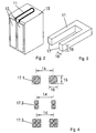
- Fig.2 shows a hairpin-shaped current conductor 11 with the Supply lines 12 on a holder 13.
- the hairpin-shaped current conductor 11 is in the holder 13 embedded and glued firmly.
- the leads 12 are also fixed to the bracket 13 connected and are located directly next to each other. So one is through the Current pulse-related change in position of the hairpin-shaped conductor 11 opposite excluded the scale. Due to the small distance between the two feed lines 12 is not an essential electromagnetic despite the position of the bracket 13 outside the shield 10 Stray field available.
- FIG. 3 An enlarged representation of the hairpin-shaped current conductor 11 is shown in FIG. 3.
- the rectangular one Cross section 17 of the current conductor 11 has the linear dimensions 15 and 16.
- this cross-section 17 of a circular conductor cross-section 17.1, of two circular conductor cross-sections 17.2 or of four circular conductor cross-sections 17.3 are taken. If there are several conductor cross sections, they are from Flows flow in the same direction. This is by connecting the individual hairpin-shaped ones in series Current conductor possible.
- the drawing with the cross section 17.2 corresponds, for example the shaped current conductor 1 in FIG. 1.
- the distance 14 between the two cross sections 17 of the hairpin-shaped current conductor 11 is substantially larger than the dimensions 15, 16 of the cross section 17.
- the field strength in FIG Plane component of the hairpin-shaped current conductor 11 is shown for different distances 24 at a current of 2200 A above the distance from the center of the hairpin-shaped current conductor 11.
- the curves 21; 22 and 23 are valid for distances 24 of 0.05 mm, 0.2 mm and 0.4 mm. Particularly for smaller distances 24, a very strong drop in the field strength can be found, for example, in the area above the center points of the conductor cross sections. There is even a change of sign.
- the curves for the different distances 24 intersect approximately at a point which is at a field strength of 2.5 10 5 A / m. If there is now a scale made of plastic-bonded ferrite, which has a coercive field strength that corresponds to the value mentioned, with its surface parallel to the hairpin-shaped current conductor, its magnetization is set in a vertical direction upwards over a length that corresponds to the distance 14, to a depth of about 0.5 mm. In addition to the distance 14, the magnetic field strength in the region near the surface of the scale with a width of less than 1 mm is large enough to set the magnetization in the opposite direction here.
- the position of the arrangement with the hairpin-shaped current conductor 11 is shifted exactly 1 mm to the right using a precise measuring arrangement.
- the direction of the current pulse that follows and therefore also that of the magnetic field is opposite to that of the first.
- the next section of the scale is magnetized vertically downwards.
- the areas of this section near the surface were magnetized in this direction already at the first pulse, so that a reversal of the direction of the magnetization already present does not have to take place.
- a field strength that exceeds the coercive field strength of the material also occurs again in the region of the first magnetized section near the surface. However, it corresponds to the direction of the magnetization inscribed there. No magnetic reversal is required.
- the lengths of the magnetized areas and also their magnetization value can thus be reproduced with high accuracy using a highly precise position measuring method for setting the position between the scale and the shaped current conductor 11.
- the cross sections 17.2 and 17.3 shown in FIG. 4 for the hairpin-shaped current conductor 11 are advantageous if there are larger distances 14 between the outgoing and return lines. By it will decrease the field strengths to too low values in the middle between the and avoided return.
- FIG. 5 shows on a bracket 13 fixed supply line 12 and shaped current conductor 18.
- FIG. 6 illustrates that this shaped current conductor is band-shaped, the width 19 is substantially larger than the thickness.
- Different ways to The cross section of the band-shaped conductor 18 is shown in FIG. 7.
- the thickness distribution 20.1 and 20.3 ensures a uniform field strength of those pointing parallel to the band Field component under the belt over most of the width 19.
- An arrangement for writing constructed in accordance with the features of the invention magnetic scales with the pulse method compared to the prior art only about 1/100 of the mass and volume, the electrical connection power is 1/100 reduced, the pulse repetition frequency and thus the effectiveness when writing scales has increased by a factor of 100 and the accuracy of the scales obtained has been increased by improved more than tenfold.
- health protection measures are no longer required in the new arrangement.
Landscapes
- Engineering & Computer Science (AREA)
- Power Engineering (AREA)
- Transmission And Conversion Of Sensor Element Output (AREA)
- Measurement Of Length, Angles, Or The Like Using Electric Or Magnetic Means (AREA)
Description
- 1
- Geformter Stromleiter
- 2
- Impulsstromquelle
- 3
- Kondensatorenbatterie
- 4
- Umschalter
- 5
- Steuereinheit
- 6
- Kondensator
- 7
- Schalter
- 8
- Anschluß Betriebsspannung
- 9
- Anschluß Steuereinheit
- 10
- Abschirmung
- 11
- Haarnadelförmiger Stromleiter
- 12
- Zuleitung
- 13
- Halterung
- 14
- Abstand
- 15
- Abmessung des Querschnitts
- 16
- Abmessung des Querschnitts
- 17
- Querschnitt
- 17.1
- Runder Querschnitt
- 17.2
- Rechteckiger Querschnitt mit zwei runden Leitern
- 17.3
- Rechteckiger Querschnitt mit vier runden Leitern
- 18
- Bandleiter
- 19
- Breite des Bandleiters
- 20.1
- Dicke des Bandleiters
- 20.2
- Dickenverteilung des Bandleiters
- 20.3
- Dicke eines zusammengesetzten Bandleiters
- 20.4
- Dicke eines zusammengesetzten Bandleiters
- 21
- Feldverlauf in 0,05 mm Abstand
- 22
- Feldverlauf in 0,2 mm Abstand
- 23
- Feldverlauf in 0,4 mm Abstand
- 24
- Abstand vom geformten Stromleiter
Claims (28)
- Anordnung zum Schreiben vom magnetischen Maßstäben, die aus Komponenten, umfassend einen geformten Stromleiter (1) zur Magnetfelderzeugung am Ort des Maßstabes und eine aus einer Kondensatorbatterie (3), einem Umschalter (4) und einer Steuereinheit (5) zusamengesetzten Impulsstromquelle (2) für beide Stromrichtungen, besteht,
dadurch gekennzeichnet, daß der geformte Stromleiter durch einen Leiter oder durch eine Leiterschleife mit jeweils an die Größe eines zu schreibenden Magnetisierungsbereiches einheitlich einzustellender Magnetisierung angepaßten Abmessungen dargestellt ist, daß der
Umschalter als H-Brücke angeordnete MOS-Transistoren aufweist und daß die Komponenten in einer starren Einheit integriert sind, die so kompakt ist, daß der durch den Umschalter geschaltete Strom durch den geformten Stromleiter in weniger als einer Mikrosekunde auf seinen Maximalwert ansteigt. - Anordnung nach Anspruch 1, dadurch gekennzeichnet, daß durch den kompakten Aufbau der Stromweg zwischen Kondensatorbatterie (3) und geformten Stromleiter (1) einen Widerstand von weniger als 50 mΩ aufweist und daß die Betriebsspannung der Anordnung im Niederspannungsbereich liegt.
- Anordnung nach Anspruch 2, dadurch gekennzeichnet, daß der geformte Stromleiter (1) zur Magnetfelderzeugung am Ort des Maßstabes einen Leitungsquerschnitt besitzt, der wesentlich kleiner ist als der Querschnitt der Zuleitungen (12) von der Kondensatorbatterie (3) bis unmittelbar zum geformten Stromleiter (1).
- Anordnung nach Anspruch 3, dadurch gekennzeichnet, daß der geformte Stromleiter (1) haamadelförmig ist und einen Querschnitt (17) hat, dessen Abmessungen wesentlich kleiner sind als der Abstand (14) der Hin- und Rückleitung.
- Anordnung nach Anspruch 4, dadurch gekennzeichnet, daß der Querschnitt (17) ein Kreis (17.1) ist.
- Anordnung nach Anspruch 5, dadurch gekennzeichnet, daß der Kreisdurchmesser 0,3 mm und der Mittenabstand (14) der Hin- und Rückleitung 1 mm beträgt.
- Anordnung nach Anspruch 4, dadurch gekennzeichnet, daß der Querschnitt (17) rechteckig ist, und daß dieser rechteckige Querschnitt (17) von zwei oder mehr runden Drähten (17.2, 17.3) eingenommen wird, wobei die einzelnen haarnadelförmigen Drähte elektrisch In Reihe geschaltet sind.
- Anordnung nach Anspruch 3, dadurch gekennzeichnet, daß der geformte Stromleiter (1) aus einem Rechteck besteht und einen Querschnitt hat, dessen Abmessungen wesentlich kleiner als Länge und Breite des Rechtecks sind.
- Anordnung nach Anspruch 8, dadurch gekennzeichnet, daß der Querschnitt ein Kreis ist.
- Anordnung nach Anspruch 8, dadurch gekennzeichnet, daß Querschnitt rechteckig ist und daß dieser rechteckige Querschnitt von zwei oder mehr rechteckigen Drähten eingenommen wird, wobei die einzelnen rechteckigen Drähte elektrisch in Reihe geschaltet sind.
- Anordnung nach Anspruch 3, dadurch gekennzeichnet, daß der geformte Stromleiter (1) aus einem Bandleiter (18) besteht, dessen Breite (19) wesentlich größer ist als seine Dicke (20.1).
- Anordnung nach Anspruch 3, dadurch gekennzeichnet, daß der geformte Stromteiter (1) aus einem Bandleiter besteht, dessen Breite wesentlich größer ist als seine Dicke (20.2), wobei die Dicke (20.2) an beiden Rändern größer ist als in der Mitte
- Anordnung nach Anspruch 3, dadurch gekennzeichnet, daß der geformte Stromleiter (1) aus einer Anzahl von unmittelbar nebeneinander liegenden Drähten (20.3) besteht.
- Anordnung nach Anspruch 3, dadurch gekennzeichnet, daß der geformte Stromleiter (1) aus einem Bandleiter und zwei unmittelbar symmetrisch neben dem Bandleiter befindlichen Drähten besteht und die drei Bestandteile ( 20.4) elektrisch in Reihe geschaltet sind.
- Anordnung nach einem der Ansprüche 3 bis 14, dadurch gekennzeichnet, daß der geformte Stromleiter (1) in einer Halterung (13) fixiert ist.
- Anordnung nach Anspruch 15, dadurch gekennzeichnet, daß der geformte Stromleiter (1) mit seiner Halterung (13) auswechselbar ist.
- Anordnung nach Anspruch 1, dadurch gekennzeichnet, daß jeder Schalter (7) aus mehreren parallel geschalteten MOS-Transistoren besteht.
- Anordnung nach Anspruch 17, dadurch gekennzeichnet, daß die Schalter (7) nach kurzer Impulszeit von wenigen Mikrosekunden durch die Steuereinheit (5) schließbar sind.
- Anordnung nach Anspruch 1, dadurch gekennzeichnet, daß die Kondensatorbatterie (3) aus Elektrolytkondensatoren (6) besteht.
- Anordnung nach Anspruch 19, dadurch gekennzeichnet, daß die Ladung der Kondensatorbatterie (3) pro Einzelimpuls nur um einen geringen Anteil vermindert wird.
- Anordnung nach Anspruch 20, dadurch gekennzeichnet, daß der geringe Anteil 5% beträgt.
- Anordnung nach Anspruch 21, dadurch gekennzeichnet, daß die Stromimpulsfolgefrequenz maximal 50 s-1 beträgt.
- Anordnung nach Anspruch 1, dadurch gekennzeichnet, daß der Versorgungsstrom der Anordnung bei Impulsströmen von 2000 A unter 500 mA liegt.
- Anordnung nach Anspruch 1, dadurch gekennzeichnet, daß sich die Impulsstromquelle (2) in einer Abschirmung (10) befindet.
- Anordnung nach Anspruch 1, dadurch gekennzeichnet, daß die Steifheit der mechanischen Konstruktion so hoch ist, daß durch die Kräfte des Impulsstromes keine Dejustierung der Position des geformten Stromleiters (1) gegenüber dem Maßstab gegeben ist.
- Verwendung einer Anordnung nach einem der Ansprüche 1 bis 25, dadurch gekennzeichnet, daß Maßstäbe mit in Meßrichtung periodischer Magnetisierung hergestellt werden.
- Verwendung einer Anordnung nach einem der Ansprüche 1 bis 25, dadurch gekennzeichnet, daß Maßstäbe mit Magnetisierungsbereichen einem Code zugeordneter Länge hergestellt werden.
- Verwendung einer Anordnung nach einem der Ansprüche 1 bis 25, dadurch gekennzeichnet, daß der geformte Stromleiter (1) berührungsfrei über dem Maßstab geführt wird.
Applications Claiming Priority (5)
| Application Number | Priority Date | Filing Date | Title |
|---|---|---|---|
| DE19909889 | 1999-03-06 | ||
| DE19909889 | 1999-03-06 | ||
| DE19940164 | 1999-08-25 | ||
| DE19940164A DE19940164A1 (de) | 1999-03-06 | 1999-08-25 | Anordnung zum Schreiben magnetischer Maßstäbe |
| PCT/EP2000/001859 WO2000054293A1 (de) | 1999-03-06 | 2000-03-03 | Anordnung zum schreiben von magnetischen massstaben |
Publications (2)
| Publication Number | Publication Date |
|---|---|
| EP1157394A1 EP1157394A1 (de) | 2001-11-28 |
| EP1157394B1 true EP1157394B1 (de) | 2004-05-19 |
Family
ID=26052223
Family Applications (1)
| Application Number | Title | Priority Date | Filing Date |
|---|---|---|---|
| EP00920470A Expired - Lifetime EP1157394B1 (de) | 1999-03-06 | 2000-03-03 | Anordnung zum schreiben von magnetischen massstäben |
Country Status (5)
| Country | Link |
|---|---|
| US (1) | US6850139B1 (de) |
| EP (1) | EP1157394B1 (de) |
| JP (1) | JP2002539438A (de) |
| AT (1) | ATE267451T1 (de) |
| WO (1) | WO2000054293A1 (de) |
Families Citing this family (41)
| Publication number | Priority date | Publication date | Assignee | Title |
|---|---|---|---|---|
| DE10313643B4 (de) * | 2003-03-26 | 2007-08-09 | Highresolution Gmbh | Positionsmesssystem |
| CA2620828A1 (en) * | 2005-09-19 | 2007-03-29 | Schweitzer Engineering Laboratories, Inc. | Method and apparatus for routing data streams among intelligent electronic devices |
| US7755872B2 (en) * | 2006-09-14 | 2010-07-13 | Schweitzer Engineering Laboratories, Inc. | System, method and device to preserve protection communication active during a bypass operation |
| DE102007063006A1 (de) * | 2007-12-21 | 2009-06-25 | Baumer Holding Ag | Verfahren und Vorrichtung zur Herstellung einer Maßverkörperung für Positionsmesssysteme sowie Maßverkörperung |
| US8760251B2 (en) | 2010-09-27 | 2014-06-24 | Correlated Magnetics Research, Llc | System and method for producing stacked field emission structures |
| US8174347B2 (en) | 2010-07-12 | 2012-05-08 | Correlated Magnetics Research, Llc | Multilevel correlated magnetic system and method for using the same |
| US9105380B2 (en) | 2008-04-04 | 2015-08-11 | Correlated Magnetics Research, Llc. | Magnetic attachment system |
| US7800471B2 (en) | 2008-04-04 | 2010-09-21 | Cedar Ridge Research, Llc | Field emission system and method |
| US9202616B2 (en) | 2009-06-02 | 2015-12-01 | Correlated Magnetics Research, Llc | Intelligent magnetic system |
| US8648681B2 (en) | 2009-06-02 | 2014-02-11 | Correlated Magnetics Research, Llc. | Magnetic structure production |
| US8373527B2 (en) | 2008-04-04 | 2013-02-12 | Correlated Magnetics Research, Llc | Magnetic attachment system |
| US8368495B2 (en) | 2008-04-04 | 2013-02-05 | Correlated Magnetics Research LLC | System and method for defining magnetic structures |
| US8816805B2 (en) | 2008-04-04 | 2014-08-26 | Correlated Magnetics Research, Llc. | Magnetic structure production |
| US8179219B2 (en) | 2008-04-04 | 2012-05-15 | Correlated Magnetics Research, Llc | Field emission system and method |
| US8279032B1 (en) | 2011-03-24 | 2012-10-02 | Correlated Magnetics Research, Llc. | System for detachment of correlated magnetic structures |
| US8576036B2 (en) | 2010-12-10 | 2013-11-05 | Correlated Magnetics Research, Llc | System and method for affecting flux of multi-pole magnetic structures |
| US8115581B2 (en) | 2008-04-04 | 2012-02-14 | Correlated Magnetics Research, Llc | Techniques for producing an electrical pulse |
| US9371923B2 (en) | 2008-04-04 | 2016-06-21 | Correlated Magnetics Research, Llc | Magnetic valve assembly |
| US8760250B2 (en) * | 2009-06-02 | 2014-06-24 | Correlated Magnetics Rsearch, LLC. | System and method for energy generation |
| US7843295B2 (en) | 2008-04-04 | 2010-11-30 | Cedar Ridge Research Llc | Magnetically attachable and detachable panel system |
| US8779879B2 (en) | 2008-04-04 | 2014-07-15 | Correlated Magnetics Research LLC | System and method for positioning a multi-pole magnetic structure |
| US8917154B2 (en) | 2012-12-10 | 2014-12-23 | Correlated Magnetics Research, Llc. | System for concentrating magnetic flux |
| US8937521B2 (en) | 2012-12-10 | 2015-01-20 | Correlated Magnetics Research, Llc. | System for concentrating magnetic flux of a multi-pole magnetic structure |
| US9257219B2 (en) | 2012-08-06 | 2016-02-09 | Correlated Magnetics Research, Llc. | System and method for magnetization |
| US8704626B2 (en) | 2010-05-10 | 2014-04-22 | Correlated Magnetics Research, Llc | System and method for moving an object |
| US9275783B2 (en) | 2012-10-15 | 2016-03-01 | Correlated Magnetics Research, Llc. | System and method for demagnetization of a magnetic structure region |
| US9404776B2 (en) | 2009-06-02 | 2016-08-02 | Correlated Magnetics Research, Llc. | System and method for tailoring polarity transitions of magnetic structures |
| KR20120095880A (ko) | 2009-09-22 | 2012-08-29 | 세다 릿지 리서치, 엘엘씨 | 멀티 레벨 상관 자기 시스템 및 이를 사용하는 방법 |
| US9711268B2 (en) | 2009-09-22 | 2017-07-18 | Correlated Magnetics Research, Llc | System and method for tailoring magnetic forces |
| US8638016B2 (en) | 2010-09-17 | 2014-01-28 | Correlated Magnetics Research, Llc | Electromagnetic structure having a core element that extends magnetic coupling around opposing surfaces of a circular magnetic structure |
| US8279031B2 (en) | 2011-01-20 | 2012-10-02 | Correlated Magnetics Research, Llc | Multi-level magnetic system for isolation of vibration |
| US8702437B2 (en) | 2011-03-24 | 2014-04-22 | Correlated Magnetics Research, Llc | Electrical adapter system |
| US9330825B2 (en) | 2011-04-12 | 2016-05-03 | Mohammad Sarai | Magnetic configurations |
| US8963380B2 (en) | 2011-07-11 | 2015-02-24 | Correlated Magnetics Research LLC. | System and method for power generation system |
| US9219403B2 (en) | 2011-09-06 | 2015-12-22 | Correlated Magnetics Research, Llc | Magnetic shear force transfer device |
| US8848973B2 (en) | 2011-09-22 | 2014-09-30 | Correlated Magnetics Research LLC | System and method for authenticating an optical pattern |
| EP2820659A4 (de) | 2012-02-28 | 2016-04-13 | Correlated Magnetics Res Llc | System zum trennen einer magnetischen struktur aus einem ferromagnetischen material |
| US9245677B2 (en) | 2012-08-06 | 2016-01-26 | Correlated Magnetics Research, Llc. | System for concentrating and controlling magnetic flux of a multi-pole magnetic structure |
| US9298281B2 (en) | 2012-12-27 | 2016-03-29 | Correlated Magnetics Research, Llc. | Magnetic vector sensor positioning and communications system |
| JP2017168707A (ja) * | 2016-03-17 | 2017-09-21 | Ntn株式会社 | 磁気エンコーダの着磁装置および着磁方法 |
| CN113823473B (zh) * | 2021-11-24 | 2022-02-08 | 宁波兴隆磁性技术有限公司 | 一种磁栅尺的覆盖式充磁方法 |
Family Cites Families (3)
| Publication number | Priority date | Publication date | Assignee | Title |
|---|---|---|---|---|
| DE907804C (de) * | 1941-10-24 | 1954-03-29 | Aeg | Einrichtung zur Magnetisierung hochwertiger Staehle unter erhoehter Temperatur |
| FR2587969B1 (fr) * | 1985-09-27 | 1991-10-11 | Thomson Csf | Dispositif de desaimantation, notamment pour batiments navals |
| DE4442682C2 (de) * | 1994-11-30 | 1997-12-18 | Bogen Electronic Gmbh | Kodierkopf zum Magnetisieren von Schichten |
-
2000
- 2000-03-03 EP EP00920470A patent/EP1157394B1/de not_active Expired - Lifetime
- 2000-03-03 JP JP2000604427A patent/JP2002539438A/ja active Pending
- 2000-03-03 AT AT00920470T patent/ATE267451T1/de not_active IP Right Cessation
- 2000-03-03 US US09/936,087 patent/US6850139B1/en not_active Expired - Fee Related
- 2000-03-03 WO PCT/EP2000/001859 patent/WO2000054293A1/de not_active Ceased
Also Published As
| Publication number | Publication date |
|---|---|
| WO2000054293A1 (de) | 2000-09-14 |
| JP2002539438A (ja) | 2002-11-19 |
| ATE267451T1 (de) | 2004-06-15 |
| US6850139B1 (en) | 2005-02-01 |
| EP1157394A1 (de) | 2001-11-28 |
Similar Documents
| Publication | Publication Date | Title |
|---|---|---|
| EP1157394A1 (de) | Anordnung zum schreiben von magnetischen massstäben | |
| DE1198599B (de) | Zweidimensionales Schieberegister | |
| DE1034689B (de) | Magnetische Speicherschaltung mit einer Platte aus magnetischem Material | |
| DE1124998B (de) | Signalgeber mit einem Hallgenerator-Abtastkopf | |
| EP0035466A1 (de) | Volumenzähler | |
| DE2120910A1 (de) | Anordnung zur Erzeugung elektrischer, von den Koordinaten in einer Ebene abhängiger Signale | |
| DE1424575B2 (de) | Magnetischer festwertspeicher | |
| DE3804786C2 (de) | ||
| DE1195971B (de) | Anordnung zur UEbertragung von Information auf ein Magnetschichtelement axialer Anisotropie | |
| DE1264508B (de) | Magnetisches Schieberegister | |
| DE69113490T2 (de) | Gerät zum Messen der Magnetfeldverteilung. | |
| DE2423836A1 (de) | Magnetaufzeichnungskopf | |
| DE19800774A1 (de) | Verfahren und magnetische Maßverkörperung zur Generierung eines Referenzsignals sowie Herstellungsverfahren für eine solche magnetische Maßverkörperung | |
| DE1045677B (de) | Verfahren und Vorrichtung, um einen oder mehrere bestimmte Magnetkoepfe fuer Aufzeichnen oder Abtasten aus einer Vielzahl hinter-einandergeschalteter Magnetkoepfe wirksam zu machen | |
| DE2743954A1 (de) | Verfahren zur messung des stroms einer fluessigkeit mittels eines induktiven stroemungsmessers | |
| DE69026997T2 (de) | Dünnfilmmagnetkopf | |
| DE6607903U (de) | Magnetkopfanordnung. | |
| DE19940164A1 (de) | Anordnung zum Schreiben magnetischer Maßstäbe | |
| DE3739111A1 (de) | Magnetfelddetektor, verfahren und schaltungsanordnung zur erzeugung eines elektrischen signals mit dem magnetfelddetektor | |
| DE2530838C3 (de) | Magnetischer Tonabnehmer | |
| EP0228579B1 (de) | Digitalisiertablett sowie Verfahren zu dessen Ansteuerung | |
| DE3008582C2 (de) | Inkrementaler Weggeber | |
| DE430701C (de) | Oszillograph zur punktweisen Aufnahme periodischer elektrischer Erscheinungen mittels kurzzeitiger Einschaltung der elektrischen Erscheinung in den Stromkreis einer Messvorrichtung | |
| DE1448881A1 (de) | Digitaler Verschluessler mit Nonius | |
| DE1499747C3 (de) | Semlpermamenter Matrixspeicher |
Legal Events
| Date | Code | Title | Description |
|---|---|---|---|
| PUAI | Public reference made under article 153(3) epc to a published international application that has entered the european phase |
Free format text: ORIGINAL CODE: 0009012 |
|
| 17P | Request for examination filed |
Effective date: 20010725 |
|
| AK | Designated contracting states |
Kind code of ref document: A1 Designated state(s): AT BE CH CY DE DK ES FI FR GB GR IE IT LI LU MC NL PT SE Kind code of ref document: A1 Designated state(s): AT CH DE FR LI |
|
| AX | Request for extension of the european patent |
Free format text: AL;LT;LV;MK;RO;SI |
|
| RIN1 | Information on inventor provided before grant (corrected) |
Inventor name: LOREIT, UWE Inventor name: DETTMANN, FRITZ Inventor name: MOELLER, CARSTEN Inventor name: SCHOENBACH, TORSTEN |
|
| GRAP | Despatch of communication of intention to grant a patent |
Free format text: ORIGINAL CODE: EPIDOSNIGR1 |
|
| GRAS | Grant fee paid |
Free format text: ORIGINAL CODE: EPIDOSNIGR3 |
|
| RAP1 | Party data changed (applicant data changed or rights of an application transferred) |
Owner name: SENSITEC GMBH |
|
| GRAA | (expected) grant |
Free format text: ORIGINAL CODE: 0009210 |
|
| AK | Designated contracting states |
Kind code of ref document: B1 Designated state(s): AT CH DE FR LI |
|
| REG | Reference to a national code |
Ref country code: CH Ref legal event code: NV Representative=s name: A. BRAUN, BRAUN, HERITIER, ESCHMANN AG PATENTANWAE Ref country code: CH Ref legal event code: EP |
|
| REG | Reference to a national code |
Ref country code: IE Ref legal event code: FG4D Free format text: GERMAN |
|
| REF | Corresponds to: |
Ref document number: 50006491 Country of ref document: DE Date of ref document: 20040624 Kind code of ref document: P |
|
| LTIE | Lt: invalidation of european patent or patent extension |
Effective date: 20040519 |
|
| ET | Fr: translation filed | ||
| REG | Reference to a national code |
Ref country code: IE Ref legal event code: FD4D |
|
| PG25 | Lapsed in a contracting state [announced via postgrant information from national office to epo] |
Ref country code: AT Free format text: LAPSE BECAUSE OF NON-PAYMENT OF DUE FEES Effective date: 20050303 |
|
| PLBE | No opposition filed within time limit |
Free format text: ORIGINAL CODE: 0009261 |
|
| STAA | Information on the status of an ep patent application or granted ep patent |
Free format text: STATUS: NO OPPOSITION FILED WITHIN TIME LIMIT |
|
| PG25 | Lapsed in a contracting state [announced via postgrant information from national office to epo] |
Ref country code: LI Free format text: LAPSE BECAUSE OF NON-PAYMENT OF DUE FEES Effective date: 20050331 Ref country code: CH Free format text: LAPSE BECAUSE OF NON-PAYMENT OF DUE FEES Effective date: 20050331 |
|
| 26N | No opposition filed |
Effective date: 20050222 |
|
| REG | Reference to a national code |
Ref country code: CH Ref legal event code: PL |
|
| PGFP | Annual fee paid to national office [announced via postgrant information from national office to epo] |
Ref country code: FR Payment date: 20060317 Year of fee payment: 7 |
|
| REG | Reference to a national code |
Ref country code: FR Ref legal event code: ST Effective date: 20071130 |
|
| PG25 | Lapsed in a contracting state [announced via postgrant information from national office to epo] |
Ref country code: FR Free format text: LAPSE BECAUSE OF NON-PAYMENT OF DUE FEES Effective date: 20070402 |
|
| REG | Reference to a national code |
Ref country code: DE Ref legal event code: R082 Ref document number: 50006491 Country of ref document: DE Representative=s name: PATENTANWAELTE DANNENBERG, SCHUBERT, GUDEL, DE Ref country code: DE Ref legal event code: R082 Ref document number: 50006491 Country of ref document: DE Representative=s name: STUMPF PATENTANWAELTE PARTGMBB, DE |
|
| REG | Reference to a national code |
Ref country code: DE Ref legal event code: R082 Ref document number: 50006491 Country of ref document: DE Representative=s name: STUMPF PATENTANWAELTE PARTGMBB, DE |
|
| PGFP | Annual fee paid to national office [announced via postgrant information from national office to epo] |
Ref country code: DE Payment date: 20190306 Year of fee payment: 20 |
|
| REG | Reference to a national code |
Ref country code: DE Ref legal event code: R071 Ref document number: 50006491 Country of ref document: DE |