EP1156532A2 - Electrode contact section of semiconductor device - Google Patents
Electrode contact section of semiconductor device Download PDFInfo
- Publication number
- EP1156532A2 EP1156532A2 EP01111239A EP01111239A EP1156532A2 EP 1156532 A2 EP1156532 A2 EP 1156532A2 EP 01111239 A EP01111239 A EP 01111239A EP 01111239 A EP01111239 A EP 01111239A EP 1156532 A2 EP1156532 A2 EP 1156532A2
- Authority
- EP
- European Patent Office
- Prior art keywords
- layer
- type
- semiconductor substrate
- contact
- electrode
- Prior art date
- Legal status (The legal status is an assumption and is not a legal conclusion. Google has not performed a legal analysis and makes no representation as to the accuracy of the status listed.)
- Withdrawn
Links
- 239000004065 semiconductor Substances 0.000 title claims abstract description 247
- 239000012535 impurity Substances 0.000 claims abstract description 229
- 239000000758 substrate Substances 0.000 claims abstract description 226
- 229910021332 silicide Inorganic materials 0.000 claims abstract description 66
- FVBUAEGBCNSCDD-UHFFFAOYSA-N silicide(4-) Chemical compound [Si-4] FVBUAEGBCNSCDD-UHFFFAOYSA-N 0.000 claims abstract description 66
- 238000002347 injection Methods 0.000 claims abstract description 57
- 239000007924 injection Substances 0.000 claims abstract description 57
- 150000002500 ions Chemical class 0.000 description 58
- IJGRMHOSHXDMSA-UHFFFAOYSA-N Atomic nitrogen Chemical compound N#N IJGRMHOSHXDMSA-UHFFFAOYSA-N 0.000 description 48
- ZOXJGFHDIHLPTG-UHFFFAOYSA-N Boron Chemical compound [B] ZOXJGFHDIHLPTG-UHFFFAOYSA-N 0.000 description 40
- 229910052796 boron Inorganic materials 0.000 description 40
- 229910015900 BF3 Inorganic materials 0.000 description 32
- WTEOIRVLGSZEPR-UHFFFAOYSA-N boron trifluoride Chemical compound FB(F)F WTEOIRVLGSZEPR-UHFFFAOYSA-N 0.000 description 32
- 238000009792 diffusion process Methods 0.000 description 26
- 229910052782 aluminium Inorganic materials 0.000 description 25
- 230000001133 acceleration Effects 0.000 description 24
- 229910052757 nitrogen Inorganic materials 0.000 description 24
- 238000005468 ion implantation Methods 0.000 description 22
- 238000002513 implantation Methods 0.000 description 16
- XAGFODPZIPBFFR-UHFFFAOYSA-N aluminium Chemical compound [Al] XAGFODPZIPBFFR-UHFFFAOYSA-N 0.000 description 13
- 229910052710 silicon Inorganic materials 0.000 description 13
- 239000010703 silicon Substances 0.000 description 13
- XUIMIQQOPSSXEZ-UHFFFAOYSA-N Silicon Chemical compound [Si] XUIMIQQOPSSXEZ-UHFFFAOYSA-N 0.000 description 9
- GUNJVIDCYZYFGV-UHFFFAOYSA-K antimony trifluoride Chemical compound F[Sb](F)F GUNJVIDCYZYFGV-UHFFFAOYSA-K 0.000 description 8
- 238000010438 heat treatment Methods 0.000 description 8
- 238000004519 manufacturing process Methods 0.000 description 8
- 238000000034 method Methods 0.000 description 8
- 238000004544 sputter deposition Methods 0.000 description 8
- 229910052751 metal Inorganic materials 0.000 description 5
- 239000002184 metal Substances 0.000 description 5
- OAICVXFJPJFONN-UHFFFAOYSA-N Phosphorus Chemical compound [P] OAICVXFJPJFONN-UHFFFAOYSA-N 0.000 description 4
- 238000007669 thermal treatment Methods 0.000 description 4
Images

Classifications
-
- H—ELECTRICITY
- H10—SEMICONDUCTOR DEVICES; ELECTRIC SOLID-STATE DEVICES NOT OTHERWISE PROVIDED FOR
- H10D—INORGANIC ELECTRIC SEMICONDUCTOR DEVICES
- H10D10/00—Bipolar junction transistors [BJT]
-
- H—ELECTRICITY
- H10—SEMICONDUCTOR DEVICES; ELECTRIC SOLID-STATE DEVICES NOT OTHERWISE PROVIDED FOR
- H10D—INORGANIC ELECTRIC SEMICONDUCTOR DEVICES
- H10D62/00—Semiconductor bodies, or regions thereof, of devices having potential barriers
- H10D62/60—Impurity distributions or concentrations
-
- H—ELECTRICITY
- H10—SEMICONDUCTOR DEVICES; ELECTRIC SOLID-STATE DEVICES NOT OTHERWISE PROVIDED FOR
- H10D—INORGANIC ELECTRIC SEMICONDUCTOR DEVICES
- H10D62/00—Semiconductor bodies, or regions thereof, of devices having potential barriers
- H10D62/10—Shapes, relative sizes or dispositions of the regions of the semiconductor bodies; Shapes of the semiconductor bodies
- H10D62/13—Semiconductor regions connected to electrodes carrying current to be rectified, amplified or switched, e.g. source or drain regions
- H10D62/141—Anode or cathode regions of thyristors; Collector or emitter regions of gated bipolar-mode devices, e.g. of IGBTs
-
- H—ELECTRICITY
- H10—SEMICONDUCTOR DEVICES; ELECTRIC SOLID-STATE DEVICES NOT OTHERWISE PROVIDED FOR
- H10D—INORGANIC ELECTRIC SEMICONDUCTOR DEVICES
- H10D62/00—Semiconductor bodies, or regions thereof, of devices having potential barriers
- H10D62/80—Semiconductor bodies, or regions thereof, of devices having potential barriers characterised by the materials
- H10D62/83—Semiconductor bodies, or regions thereof, of devices having potential barriers characterised by the materials being Group IV materials, e.g. B-doped Si or undoped Ge
-
- H—ELECTRICITY
- H10—SEMICONDUCTOR DEVICES; ELECTRIC SOLID-STATE DEVICES NOT OTHERWISE PROVIDED FOR
- H10D—INORGANIC ELECTRIC SEMICONDUCTOR DEVICES
- H10D62/00—Semiconductor bodies, or regions thereof, of devices having potential barriers
- H10D62/80—Semiconductor bodies, or regions thereof, of devices having potential barriers characterised by the materials
- H10D62/83—Semiconductor bodies, or regions thereof, of devices having potential barriers characterised by the materials being Group IV materials, e.g. B-doped Si or undoped Ge
- H10D62/834—Semiconductor bodies, or regions thereof, of devices having potential barriers characterised by the materials being Group IV materials, e.g. B-doped Si or undoped Ge further characterised by the dopants
-
- H—ELECTRICITY
- H10—SEMICONDUCTOR DEVICES; ELECTRIC SOLID-STATE DEVICES NOT OTHERWISE PROVIDED FOR
- H10D—INORGANIC ELECTRIC SEMICONDUCTOR DEVICES
- H10D64/00—Electrodes of devices having potential barriers
- H10D64/60—Electrodes characterised by their materials
- H10D64/62—Electrodes ohmically coupled to a semiconductor
Definitions
- the present invention relates to an electrode contact section incorporated in a semiconductor device.
- en electrode section incorporated in a semiconductor device is formed of an impurity layer provided in a semiconductor layer, and an electrode (made of, for example, a metal such as aluminum) that is in contact with the impurity layer.
- the impurity layer is often formed by ion implantation for the purpose of low cost.
- the concentration of an impurity in the impurity layer is generally increased.
- the concentration profile of the impurity layer shows a curved line with a peak.
- the impurity concentration of a surface portion of the semiconductor layer is lower than a peak concentration assumed at an inner portion thereof.
- a longitudinal power device such as an IGBT
- an impurity layer is provided at the other surface thereof.
- the impurity layer at the other surface of the semiconductor layer cannot be annealed at a high temperature for a long time, with the result that the difference between the peak concentration and the surface concentration of the impurity layer is increased, and hence the contact resistance cannot sufficiently be reduced.
- an IGBT Insulated Gate Bipolar Transistor
- an electrode contact section a contact section between the impurity layer 2 and an anode layer 3
- the present invention has been may provided an electrode contact section of a sufficiently low contact resistance even when forming an impurity layer by ion implantation.
- the invention has been may provided an electrode contact section in which the contact resistance and the carrier injection coefficient can simultaneously be reduced.
- an electrode contact section incorporated in a semiconductor device, comprising: a first-conductivity-type semiconductor substrate; a second-conductivity-type impurity layer formed in one surface of the semiconductor substrate and having a thickness of not more than 1.0 ⁇ m from a surface of the semiconductor substrate; a second-conductivity-type contact layer formed in the impurity layer and having a thickness of not more than 0.2 ⁇ m from the surface of the semiconductor substrate, the contact layer being thinner than the impurity layer and having a higher impurity concentration than the impurity layer; and a first electrode formed on the contact layer.
- an electrode contact section incorporated in a semiconductor device, comprising: a first-conductivity-type semiconductor substrate; a second-conductivity-type impurity layer formed in one surface of the semiconductor substrate; a second-conductivity-type contact layer formed in the impurity layer, being thinner than the impurity layer and having a higher impurity concentration than the impurity layer; a first electrode formed on the contact layer; and a silicide layer formed between the first electrode and the contact layer, the silicide layer having a contact-layer-side end thereof made to substantially correspond to that portion of the contact layer, at which a concentration profile of the contact layer assumes a peak value.
- Electrode contact sections each incorporated in a semiconductor device according to the present invention will be described in detail with reference to the accompanying drawings.
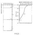
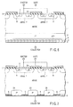
- FIG. 2 shows an electrode contact section incorporated as an example in a semiconductor device according to the invention.
- a p-type impurity layer 2 is formed in an n-type semiconductor substrate 1.
- the n-type semiconductor layer 1 contains an n-type impurity such as phosphor (P) with a substantially constant concentration of approx. 10 14 ions/cm 3 .
- the p-type impurity layer 2 is formed in a surface area of the semiconductor substrate 1 and contains a p-type impurity such as boron (B).
- the depth of the p-type impurity layer 2 from the surface of the semiconductor substrate 1 is set at 1.0 ⁇ m or less, for example, approx. 0.8 ⁇ m. Further, the peak value of the concentration profile of the p-type impurity layer 2 is set at a value falling within the range of 10 17 - 10 18 ions/cm 3 .
- a p + -type contact layer 4 is formed in the p-type impurity layer 2, and an electrode 3 is formed on the p + -type contact layer 4.
- the p + -type contact layer 4 is thus interposed between the p-type impurity layer 2 and the electrode 3 and has a higher impurity concentration than the p-type impurity layer 2.
- the p + -type contact layer 4 contains a p-type impurity such as boron (B) or boron fluoride (BF 2 ), etc., and has an impurity concentration peak value of 10 19 ions/cm 3 or more and a surface impurity concentration of 10 18 ions/cm 3 or more.
- the depth of the p + -type contact layer 4 from the surface of the semiconductor substrate 1 is set at 0.2 ⁇ m or less, for example, approx. 0.16 ⁇ m.
- the electrode 3 is formed of, for example, aluminum.
- the p-type impurity layer 2 has a low impurity concentration, and a sufficiently shallow depth of 1.0 ⁇ m or less from the surface of the semiconductor substrate 1. Accordingly, when this electrode contact structure is applied to the collector (anode) electrode of an IGBT, the coefficient of carrier (positive hole) injection at the time of turning off the semiconductor device can be reduced, thereby increasing the speed of the turn-off operation.
- the p + -type contact layer 4 having a higher impurity concentration than the p-type impurity layer 2 is provided between the p-type impurity layer 2 and the electrode 3. Since the depth of the p + -type contact layer 4 from the surface of the semiconductor substrate 1 is set at 0.2 ⁇ m or less, the p + -type contact layer 4 does not influence the carrier injection coefficient at the time of turning off the semiconductor device. In other words, the p + -type contact layer 4 does not increase the carrier injection coefficient.
- the contact resistance at the electrode contact section can be reduced.
- the electrode contact section of the invention can have a sufficiently low contact resistance, and simultaneously realize a low carrier injection coefficient when turning off the semiconductor device.
- the semiconductor substrate 1 is of the n-type and the impurity layer 2 and the p + -type contact layer 4 are of the p-type, a similar advantage can be obtained if the semiconductor substrate 1 is made to be of the p-type and the impurity layer 2 and the p + -type contact layer 4 are made to be of the n-type.
- an n-type semiconductor substrate e.g. a silicon substrate 1 having, for example, an impurity concentration of approx. 1.5 ⁇ 10 14 ions/cm 2 is prepared.
- a p-type impurity such as boron (B) is implanted into the semiconductor substrate by ion implantation.
- the acceleration voltage and the dose, as implantation conditions are set at, for example, approx. 60 keV and approx. 1 ⁇ 10 13 ions/cm 2 , respectively.
- the resultant structure is subjected to a thermal diffusion process executed in the atmosphere of nitrogen of approx. 1050°C for approx. 20 min.
- a p-type impurity layer e.g. a p-type emitter layer 2 having a depth of approx. 0.8 ⁇ m from the surface of the semiconductor substrate 1 is formed.
- a p-type impurity such as boron (B) is implanted into the p-type impurity layer 2 in the semiconductor substrate 1 by ion implantation.
- the acceleration voltage and the dose, as implantation conditions are set at, for example, approx. 10 keV and approx. 1 ⁇ 10 14 ions/cm 2 , respectively.
- the resultant structure is subjected to a thermal diffusion process executed in the atmosphere of nitrogen of approx. 800°C for approx. 30 min.
- a p + -type contact layer 4 having a depth of approx. 0.16 ⁇ m from the surface of the semiconductor substrate 1 is formed.
- the p + -type contact layer 4 must be formed very shallow, and must have a very high impurity concentration. To this end, the acceleration voltage is set low, the dose is set high, and the period for executing the thermal diffusion process is set short, as is described above.
- Boron fluoride for example, may be used as the p-type impurity, instead of boron (B) (i.e. the element is changed from a light one to a heavy one), and implanted into the p-type impurity layer 2 in the semiconductor substrate 1, thereby forming a p + -type contact layer 4.
- B boron
- a thermal oxide film formed on a surface portion of the semiconductor substrate 1, i.e. on a surface portion of the p + -type contact layer 4, is removed using antimony fluoride.
- the electrode 3 made of a metal such as aluminum is provided on the p + -type contact layer 4 by sputtering or CVD.
- the resultant structure is subjected to a heat treatment executed for approx. 30 min. in the atmosphere of nitrogen of approx. 450°C, thereby diffusing the atoms (e.g. aluminum atoms) of the electrode 3 into the semiconductor substrate 1, i.e. into the p + -type contact layer 4 so as to reduce the contact resistance of the electrode 3 and the p + -type contact layer 4.
- atoms e.g. aluminum atoms
- the depth and impurity concentration of the p-type impurity layer 2 substantially determine the carrier injection coefficient.
- the peak value of the impurity concentration profile of the p-type impurity layer 2 falls within the range of 10 17 - 10 18 ions/cm 3 , and the depth of the layer 2 is set at a sufficiently low value of 1.0 ⁇ m or less. Accordingly, if this structure is applied to the collector electrode of an IGBT, the carrier injection coefficient when turning off the IGBT can be reduced, thereby increasing the speed of the turn-off operation.
- the p + -type contact layer 4 which has a higher impurity concentration than the p-type impurity layer 2 and is provided between the p-type impurity layer 2 and the electrode 3, is set to have a depth of 0.2 ⁇ m or less from the surface of the semiconductor substrate 1, it does not influence the carrier injection coefficient at the time of turning off the semiconductor device. In other words, the p + -type contact layer 4 does not increase the carrier injection coefficient. Further, since the peak value of the impurity concentration profile of the p + -type contact layer 4 is set at approx. 10 19 ions/cm 3 , the contact resistance of the electrode contact section is also reduced.
- the p-type impurity layer 2 is made to be sufficiently shallow (1.0 ⁇ m or less) and have a low concentration (10 17 - 10 18 ions/cm 3 ), and the p + -type contact layer 4 interposed between the p-type impurity layer 2 and the electrode 3 has a sufficiently high impurity concentration (approx. 10 19 ions/cm 3 ).
- This structure simultaneously realizes a low contact resistance and a low carrier injection coefficient.
- a silicide layer 5 is formed between the electrode 3 and the p + -type contact layer 4.
- This example is not characterized by the provision of the silicide layer 5, but by the depth of the silicide layer 5 from the surface of the semiconductor substrate 1, more specifically, by the relationship between the depth of the silicide layer 5 from the surface of the semiconductor substrate 1, and the peak value of the impurity profile of the p + -type contact layer 4.
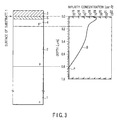
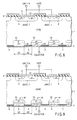
- FIG. 3 shows the second example.
- a p-type impurity layer 2 is formed in an n-type semiconductor substrate 1.
- the n-type semiconductor layer 1 contains an n-type impurity such as phosphor (P) with a substantially constant concentration of approx. 10 14 ions/cm 3 .
- the p-type impurity layer 2 is formed in a surface area of the semiconductor substrate 1 and contains a p-type impurity such as boron (B).
- the depth of the p-type impurity layer 2 from the surface of the semiconductor substrate 1 is set at 1.0 ⁇ m or less, for example, approx. 0.8 ⁇ m. Further, the peak value of the concentration profile of the p-type impurity layer 2 is set at a value falling within the range of 10 17 - 10 18 ions/cm 3 .
- a p + -type contact layer 4 is formed in the p-type impurity layer 2, and an electrode 3 is formed on the p + -type contact layer 4.
- the p + -type contact layer 4 is thus interposed between the p-type impurity layer 2 and the electrode 3 and has a higher impurity concentration than the p-type impurity layer 2.
- the p + -type contact layer 4 contains a p-type impurity such as boron (B) or boron fluoride (BF 2 ), etc., and has an impurity concentration peak value of 10 19 ions/cm 3 or more and a surface impurity concentration of 10 18 ions/cm 3 or more.
- the depth of the p + -type contact layer 4 from the surface of the semiconductor substrate 1 is set at 0.2 ⁇ m or less, for example, approx. 0.16 ⁇ m.
- the electrode 3 is formed of, for example, aluminum.
- a silicide layer 5 is provided between the electrode 3 and the p + -type contact layer 4.
- the silicide layer 5 is formed by, for example, a thermal treatment in which atoms (e.g. aluminum atoms) constituting the electrode 3 react with atoms (silicon atoms) constituting the semiconductor substrate 1.
- the depth of the silicide layer 5 from the surface of the semiconductor substrate 1 is set equal to or shallower than the depth of the p + -type contact layer 4 from the surface of the semiconductor substrate 1. In this example, since the depth of the p + -type contact layer 4 from the surface of the semiconductor substrate 1 is set at 0.2 ⁇ m or less, the depth of the silicide layer 5 from the surface of the semiconductor substrate 1 is also set at 0.2 ⁇ m or less.
- the electrode 3 is electrically connected to the lowest resistance portion of the p + -type contact layer 4 (corresponding to a portion thereof at which the concentration profile assumes the peak value) via the silicide layer 5, thereby reducing the contact resistance.
- the p-type impurity layer 2 has a low impurity concentration, and a sufficiently shallow depth of 1.0 ⁇ m or less from the surface of the semiconductor substrate 1. Accordingly, if this electrode contact structure is applied to the collector electrode (anode electrode) of an IGBT, the carrier (positive hole) injection coefficient when turning off the IGBT can be reduced, thereby increasing the speed of the turn-off operation.
- the p + -type contact layer 4 which has a higher impurity concentration than the p-type impurity layer 2 and is provided between the p-type impurity layer 2 and the electrode 3, is set to have a depth of 0.2 ⁇ m or less from the surface of the semiconductor substrate 1, it does not influence the carrier injection coefficient at the time of turning off the semiconductor device. In other words, the p + -type contact layer 4 does not increase the carrier injection coefficient.
- the p + -type contact layer 4 has a sufficiently high impurity concentration
- the silicide layer 5 is provided between the electrode 3 and the p + -type contact layer 4.
- the position of the bottom of the silicide layer 5 is made to correspond to that portion of the p + -type contact layer 4, at which the concentration profile of the layer 4 assumes a peak value. Accordingly, the contact resistance of the electrode contact section is further reduced.
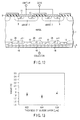
- FIG. 13 shows the relationship between a saturation voltage Vce (sat) between the collector and the emitter and the thickness of the silicide layer 5 (the depth from the surface of the semiconductor substrate 1), obtained when the concentration profile of the p + -type contact layer 4 assumes a peak value at a depth of 0.04 ⁇ m from the surface of the semiconductor substrate 1.
- the saturation voltage Vce (sat) between the collector and the emitter is minimum when the position of the bottom of the silicide layer 5 (i.e. the thickness of the layer 5) corresponds to that portion of the p + -type contact layer 4, at which the concentration profile of the layer 4 assumes the peak value, i.e., when the thickness of the layer 5 is 0.04 ⁇ m.
- the contact resistance is minimum when the position of the bottom of the silicide layer 5 (i.e. the thickness of the layer 5) corresponds to that portion of the p + -type contact layer 4, at which the concentration profile of the layer 4 assumes the peak value.
- the electrode contact section of the invention simultaneously realizes a low contact resistance and a low carrier injection coefficient.
- the semiconductor substrate 1 is of the n-type and the impurity layer 2 and the contact layer 4 are of the p-type, the same advantage can be obtained by making the semiconductor substrate 1 be of the p-type and the impurity layer 2 and the contact layer 4 be of the n-type.
- an n-type semiconductor substrate e.g. a silicon substrate 1 having, for example, an impurity concentration of approx. 1.5 ⁇ 10 14 ions/cm 2 is prepared.
- a p-type impurity such as boron (B) is implanted into the semiconductor substrate by ion implantation.
- the acceleration voltage and the dose, as implantation conditions are set at, for example, approx. 60 keV and approx. 1 ⁇ 10 13 ions/cm 2 , respectively.
- the resultant structure is subjected to a thermal diffusion process executed in the atmosphere of nitrogen of approx. 1050°C for approx. 20 min.
- a p-type impurity layer e.g. a p-type emitter layer 2 having a depth of approx. 0.8 ⁇ m from the surface of the semiconductor substrate 1 is formed.
- a p-type impurity such as boron (B) is implanted into the p-type impurity layer 2 in the semiconductor substrate 1 by ion implantation.
- the acceleration voltage and the dose, as implantation conditions are set at, for example, approx. 10 keV and approx. 1 ⁇ 10 14 ions/cm 2 , respectively.
- the resultant structure is subjected to a thermal diffusion process executed in the atmosphere of nitrogen of approx. 800°C for approx. 30 min.
- a p + -type contact layer 4 having a depth of approx. 0.16 ⁇ m from the surface of the semiconductor substrate 1 is formed.
- the p + -type contact layer 4 must be formed very shallow, and must have a very high impurity concentration. To this end, the acceleration voltage is set low, the dose is set high, and the period for executing the thermal diffusion process is set short, as is described above.
- Boron fluoride for example, may be used as the p-type impurity, instead of boron (B) (i.e. the element is changed from a light one to a heavy one), and implanted into the p-type impurity layer 2 in the semiconductor substrate 1, thereby forming a p + -type contact layer 4.
- B boron
- a thermal oxide film formed on a surface portion of the semiconductor substrate 1, i.e. on a surface portion of the p + -type contact layer 4, is removed using antimony fluoride.
- an electrode 3 made of a metal such as aluminum and having a thickness of approx. 0.05 ⁇ m is provided on the p + -type contact layer 4 by sputtering or CVD.
- the resultant structure is subjected to a heat treatment executed for approx. 30 min. in the atmosphere of nitrogen of approx. 450°C, thereby diffusing the atoms (e.g. aluminum atoms) of the electrode 3 into the semiconductor substrate 1, i.e. into the p + -type contact layer 4.
- a silicide layer 5 is formed.
- the thickness of the silicide layer 5 (the depth from the surface of the semiconductor substrate 1) is made substantially equal to that thickness of the p + -type contact layer 4 from the surface of the semiconductor substrate 1, at which the concentration profile of the layer 4 assumes a peak value.
- the silicide layer 5 is made to have a thickness of approx. 0.04 ⁇ m.
- the contact resistance between the electrode 3 and the p-type impurity layer 2 in the electrode contact section is minimized.
- the carrier injection coefficient is basically determined from the depth and impurity concentration of the p-type impurity layer 2.
- the peak value of the concentration profile of the p-type impurity layer 2 is set at a value falling within the range of 10 17 - 10 18 ions/cm 3 .
- the depth of the p-type impurity layer 2 from the surface of the semiconductor substrate 1 is set at a sufficient low value of 1.0 ⁇ m or less. Accordingly, when this electrode contact structure is applied to the collector electrode of an IGBT, the coefficient of carrier injection at the time of turning off the semiconductor device can be reduced, thereby increasing the speed of the turn-off operation.
- the p + -type contact layer 4 having a higher impurity concentration than the p-type impurity layer 2 is provided between the p-type impurity layer 2 and the electrode 3. Since the depth of the p + -type contact layer 4 from the surface of the semiconductor substrate 1 is set at 0.2 ⁇ m or less, the p + -type contact layer 4 does not influence the carrier injection coefficient at the time of turning off the semiconductor device. In other words, the p + -type contact layer 4 does not increase the carrier injection coefficient. Moreover, since the peak value of the impurity concentration profile of the p + -type contact layer 4 is set at approx. 10 19 ions/cm 3 , the contact resistance of the electrode contact section is also reduced.
- the p + -type contact layer 4 has a sufficiently high impurity concentration
- the silicide layer 5 is provided between the electrode 3 and the p + -type contact layer 4. Further, the position of the bottom of the silicide layer 5 is made to correspond to that portion of the p + -type contact layer 4, at which the concentration profile of the layer 4 assumes a peak value. Accordingly, the contact resistance of the electrode contact section is further reduced.
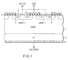
- FIG. 4 shows a general structure for the IGBT.
- An n-type semiconductor substrate (silicon substrate) 1 serves as an n-type base layer.
- a p-type base layer 7 is formed on one surface of the semiconductor substrate 1, and an n + -type emitter layer 8 is formed in the p-type base layer 7.
- a gate electrode 10 is formed on the p-type base layer (channel section) 7 between the n-type base layer 1 and the n + -type emitter layer 8, with an insulating layer 9 interposed therebetween. Further, an emitter electrode 11 is formed on the p-type base layer 7 and the n + -type emitter layer 8.
- a p + -type emitter layer 2 is formed on the other surface of the semiconductor substrate 1.
- the p + -type emitter layer 2 serves as a p-type impurity layer that constitutes an electrode contact section according to the invention.
- a collector electrode 3 is formed on the p + -type emitter layer 2.
- the IGBT it is important to reduce the contact resistance of the p + -type emitter layer 2 and the collector electrode 3, and also to reduce the coefficient of carrier (positive hole) injection from the p + -type emitter layer 2 to the n-type base layer 1 so as to increase the speed of the turn-off operation.
- the application of the electrode contact structure of the invention to the IGBT enables the simultaneous realization of a reduction of the contact resistance and the carrier injection coefficient.
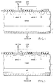
- FIG. 5 shows an IGBT as a first example of the invention.
- This example relates to an IGBT to which the above-described first electrode contact section is applied.
- a p-type base layer 7 is formed on one surface of an n-type semiconductor substrate (n-type base layer) 1, and an n + -type emitter layer 8 is formed in the p-type base layer 7.
- a gate electrode 10 is formed on the p-type base layer (channel section) 7 between the n-type base layer 1 and the n + -type emitter layer 8, with an insulating layer 9 interposed therebetween.
- an emitter electrode 11 is formed on the p-type base layer 7 and the n + -type emitter layer 8.
- a p + -type emitter layer 2 is formed on the other surface of the semiconductor substrate 1.
- the p + -type emitter layer 2 contains a p-type impurity such as boron (B).
- the depth of the p + -type emitter layer 2 from the other surface of the semiconductor substrate 1 is set at 1.0 ⁇ m or less, for example, approx. 0.8 ⁇ m. Further, the peak value of the concentration profile of the p + -type emitter layer 2 is set at a value falling within the range of 10 17 - 10 18 ions/cm 3 .
- a p ++ -type contact layer 4 is formed in the p + -type emitter layer 2, and a collector electrode 3 is formed on the p ++ -type contact layer 4.
- the p ++ -type contact layer 4 is thus interposed between the p + -type emitter layer 2 and the collector electrode 3 and has a higher impurity concentration than the p + -type emitter layer 2.
- the p ++ -type contact layer 4 contains a p-type impurity such as boron (B) or boron fluoride (BF 2 ), etc., and has an impurity concentration peak value of 10 19 ions/cm 3 or more and a surface impurity concentration of 10 18 ions/cm 3 or more.
- the depth of the p ++ -type contact layer 4 from the surface of the semiconductor substrate 1 is set at 0.2 ⁇ m or less, for example, approx. 0.16 ⁇ m.
- the collector electrode 3 is formed of, for example, aluminum.
- the p + -type emitter layer 2 has a low impurity concentration, and a sufficiently shallow depth of 1.0 ⁇ m or less from the surface of the semiconductor substrate 1. Accordingly, the coefficient of carrier (positive hole) injection at the time of turning off the IGBT can be reduced, thereby increasing the speed of the turn-off operation.
- the p ++ -type contact layer 4 having a higher impurity concentration than the p + -type emitter layer 2 is provided between the p + -type emitter layer 2 and the collector electrode 3. Since the depth of the p ++ -type contact layer 4 from the surface of the semiconductor substrate 1 is set at 0.2 ⁇ m or less, the p + -type contact layer 4 does not influence the carrier injection coefficient at the time of turning off the IGBT. In other words, the p ++ -type contact layer 4 does not increase the carrier injection coefficient.
- the contact resistance of the electrode contact section is reduced.
- the electrode contact section of the IGBT enables the simultaneous realization of a sufficient reduction of the contact resistance and reduction of the carrier injection coefficient.
- the semiconductor substrate 1 is of the n-type and the emitter layer 2 and the contact layer 4 are of the p-type, the same advantage can be obtained by making the semiconductor substrate 1 be of the p-type and the emitter layer 2 and the contact layer 4 be of the n-type.
- an n-type semiconductor substrate e.g. a silicon substrate 1 having, for example, an impurity concentration of approx. 1.5 ⁇ 10 14 ions/cm 2 is prepared.
- a p-type impurity such as boron (B) is implanted into the other surface of the semiconductor substrate 1 by ion implantation.
- the acceleration voltage and the dose, as implantation conditions are set at, for example, approx. 60 keV and approx. 1 ⁇ 10 13 ions/cm 2 , respectively.
- the resultant structure is subjected to a thermal diffusion process executed in the atmosphere of nitrogen of approx. 1050°C for approx. 20 min.
- a p + -type emitter layer 2 having a depth of approx. 0.8 ⁇ m from the other surface of the semiconductor substrate 1 is formed.
- a p-type impurity such as boron (B) is implanted into the p + -type emitter layer 2 in the other surface of the semiconductor substrate 1 by ion implantation.
- the acceleration voltage and the dose, as implantation conditions are set at, for example, approx. 10 keV and approx. 1 ⁇ 10 14 ions/cm 2 , respectively.
- the resultant structure is subjected to a thermal diffusion process executed in the atmosphere of nitrogen of approx. 800°C for approx. 30 min.
- a p ++ -type contact layer 4 having a depth of approx. 0.16 ⁇ m from the other surface of the semiconductor substrate 1 is formed.
- the p ++ -type contact layer 4 must be formed very shallow, and must have a very high impurity concentration. To this end, the acceleration voltage is set low, the dose is set high, and the period for executing the thermal diffusion process is set short, as is described above.
- Boron fluoride for example, may be used as the p-type impurity, instead of boron (B) (i.e. the element is changed from a light one to a heavy one), and implanted into the p + -type emitter layer 2 in the semiconductor substrate 1, thereby forming a p ++ -type contact layer 4.
- B boron
- a collector electrode 3 made of a metal such as aluminum is provided on the p ++ -type contact layer 4 by sputtering or CVD.
- the resultant structure is subjected to a heat treatment executed for approx. 30 min. in the atmosphere of nitrogen of approx. 450°C, thereby diffusing the atoms (e.g. aluminum atoms) of the collector electrode 3 into the semiconductor substrate 1, i.e. into the p ++ -type contact layer 4 so as to reduce the contact resistance of the collector electrode 3 and the p ++ -type contact layer 4.
- atoms e.g. aluminum atoms
- FIG. 6 shows an IGBT as a second example of the invention.
- This example relates to an IGBT to which the above-described second electrode contact section is applied.
- a p-type base layer 7 is formed on one surface of an n-type semiconductor substrate (n-type base layer) 1, and an n + -type emitter layer 8 is formed in the p-type base layer 7.
- a gate electrode 10 is formed on the p-type base layer (channel section) 7 between the n-type base layer 1 and the n + -type emitter layer 8, with an insulating layer 9 interposed therebetween.
- an emitter electrode 11 is formed on the p-type base layer 7 and the n + -type emitter layer 8.
- a p + -type emitter layer 2 is formed on the other surface of the semiconductor substrate 1.
- the p + -type emitter layer 2 contains a p-type impurity such as boron (B).
- the depth of the p + -type emitter layer 2 from the other surface of the semiconductor substrate 1 is set at 1.0 ⁇ m or less, for example, approx. 0.8 ⁇ m. Further, the peak value of the concentration profile of the p + -type emitter layer 2 is set at a value falling within the range of 10 17 - 10 18 ions/cm 3 .
- a p ++ -type contact layer 4 is formed in the p + -type emitter layer 2, and a collector electrode 3 is formed on the p ++ -type contact layer 4.
- the p ++ -type contact layer 4 is thus interposed between the p + -type emitter layer 2 and the collector electrode 3 and has a higher impurity concentration than the p + -type emitter layer 2.
- the p ++ -type contact layer 4 contains a p-type impurity such as boron (B) or boron fluoride (BF 2 ), etc., and has an impurity concentration peak value of 10 19 ions/cm 3 or more and a surface impurity concentration of 10 18 ions/cm 3 or more.
- the depth of the p ++ -type contact layer 4 from the surface of the semiconductor substrate 1 is set at 0.2 ⁇ m or less, for example, approx. 0.16 ⁇ m.
- the collector electrode 3 is formed of, for example, aluminum.
- a silicide layer 5 is provided between the collector electrode 3 and the p ++ -type contact layer 4.
- the silicide layer 5 is formed by, for example, a thermal treatment in which atoms (e.g. aluminum atoms) constituting the collector electrode 3 react with atoms (silicon atoms) constituting the semiconductor substrate 1.
- the depth of the silicide layer 5 from the other surface of the semiconductor substrate 1 is set equal to or shallower than the depth of the p ++ -type contact layer 4 from the other surface of the semiconductor substrate 1.
- the depth of the silicide layer 5 from the other surface of the semiconductor substrate 1 is also set at 0.2 ⁇ m or less.
- the collector electrode 3 is electrically connected to the lowest resistance portion of the p ++ -type contact layer 4 (corresponding to a portion thereof at which the concentration profile assumes the peak value) via the silicide layer 5, thereby reducing the contact resistance.
- the p + -type emitter layer 2 has a low impurity concentration, and a sufficiently shallow depth of 1.0 ⁇ m or less from the other surface of the semiconductor substrate 1. Accordingly, the carrier (positive hole) injection coefficient when turning off the IGBT can be reduced, thereby increasing the speed of the turn-off operation.
- the p ++ -type contact layer 4 which has a higher impurity concentration than the p + -type emitter layer 2 and is provided between the p + -type emitter layer 2 and the collector electrode 3, is set to have a depth of 0.2 ⁇ m or less from the surface of the semiconductor substrate 1, it does not influence the carrier injection coefficient at the time of turning off the IGBT. In other words, the p ++ -type contact layer 4 does not increase the carrier injection coefficient.
- the p ++ -type contact layer 4 has a sufficiently high impurity concentration
- the silicide layer 5 is provided between the collector electrode 3 and the p ++ -type contact layer 4.
- the position of the bottom of the silicide layer 5 is made to correspond to that portion of the p ++ -type contact layer 4, at which the concentration profile of the layer 4 assumes a peak value. Accordingly, the contact resistance of the electrode contact section is further reduced.
- the electrode contact section of the IGBT according to the invention enables the simultaneous realization of a sufficient reduction of the contact resistance and reduction of the carrier injection coefficient.
- the semiconductor substrate 1 is of the n-type and the emitter layer 2 and the contact layer 4 are of the p-type, the same advantage can be obtained by making the semiconductor substrate 1 be of the p-type and the emitter layer 2 and the contact layer 4 be of the n-type.
- an n-type semiconductor substrate e.g. a silicon substrate 1 having, for example, an impurity concentration of approx. 1.5 ⁇ 10 14 ions/cm 2 is prepared.
- a p-type impurity such as boron (B) is implanted into the other surface of the semiconductor substrate 1 by ion implantation.
- the acceleration voltage and the dose, as implantation conditions are set at, for example, approx. 60 keV and approx. 1 ⁇ 10 13 ions/cm 2 , respectively.
- the resultant structure is subjected to a thermal diffusion process executed in the atmosphere of nitrogen of approx. 1050°C for approx. 20 min.
- a p + -type emitter layer 2 having a depth of approx. 0.8 ⁇ m from the other surface of the semiconductor substrate 1 is formed.
- a p-type impurity such as boron (B) is implanted into the p + -type emitter layer 2 in the other surface of the semiconductor substrate 1 by ion implantation.
- the acceleration voltage and the dose, as implantation conditions are set at, for example, approx. 10 keV and approx. 1 ⁇ 10 14 ions/cm 2 , respectively.
- the resultant structure is subjected to a thermal diffusion process executed in the atmosphere of nitrogen of approx. 800°C for approx. 30 min.
- a p ++ -type contact layer 4 having a depth of approx. 0.16 ⁇ m from the other surface of the semiconductor substrate 1 is formed.
- the p ++ -type contact layer 4 must be formed very shallow, and must have a very high impurity concentration. To this end, the acceleration voltage is set low, the dose is set high, and the period for executing the thermal diffusion process is set short, as is described above.
- Boron fluoride for example, may be used as the p-type impurity, instead of boron (B) (i.e. the element is changed from a light one to a heavy one), and implanted into the p + -type emitter layer 2 in the semiconductor substrate 1, thereby forming a p ++ -type contact layer 4.
- B boron
- a collector electrode 3 made of a metal such as aluminum and having a thickness of approx. 0.05 ⁇ m is provided on the p ++ -type contact layer 4 by sputtering or CVD.
- the resultant structure is subjected to a heat treatment executed for approx. 30 min. in the atmosphere of nitrogen of approx. 450°C, thereby diffusing the atoms (e.g. aluminum atoms) of the collector electrode 3 into the semiconductor substrate 1, i.e. into the p ++ -type contact layer 4 so as to form a silicide layer 5.
- the thickness of the silicide layer 5 (the depth from the other surface of the semiconductor substrate 1) is made substantially equal to that thickness of the p ++ -type contact layer 4 from the other surface of the semiconductor substrate 1, at which the concentration profile of the layer 4 assumes a peak value.
- the silicide layer 5 is made to have a thickness of approx. 0.04 ⁇ m.
- the collector electrode 3 may be formed after forming the silicide layer 5.
- FIG. 8 shows an IGBT as a third example of the invention.
- This example relates to an IGBT (a reference example) as shown in FIG. 7, in which a plurality of p + -type emitter layers 2A isolated from each other are formed, and to which the above-described first electrode contact section is applied.
- a p-type base layer 7 is formed on one surface of an n-type semiconductor substrate (n-type base layer) 1, and an n + -type emitter layer 8 is formed in the p-type base layer 7.
- a gate electrode 10 is formed on the p-type base layer (channel section) 7 between the n-type base layer 1 and the n + -type emitter layer 8, with an insulating layer 9 interposed therebetween.
- an emitter electrode 11 is formed on the p-type base layer 7 and the n + -type emitter layer 8.
- a plurality of p + -type emitter layers 2A isolated from each other are formed on the other surface of the semiconductor substrate 1.
- Each p + -type emitter layer 2A contains a p-type impurity such as boron (B).
- the depth of each p + -type emitter layer 2A from the other surface of the semiconductor substrate 1 is set at 1.0 ⁇ m or less, for example, approx. 0.8 ⁇ m.
- the peak value of the concentration profile of each p + -type emitter layer 2A is set at a value falling within the range of 10 17 - 10 18 ions/cm 3 .
- a p ++ -type contact layer 4A is formed in each p + -type emitter layer 2A, and a collector electrode 3 is formed on the resultant p ++ -type contact layers 4A. Further, insulating films 6 are formed on respective exposed portions of the other surface of the n-type base layer (semiconductor substrate) 1. Accordingly, the collector electrode 3 is electrically connected to the plurality of p + -type emitter layers 2A, and electrically isolated from the n-type base layer 1.
- the p ++ -type contact layers 4A are interposed between the respective p + -type emitter layers 2A and the collector electrode 3, and have a higher impurity concentration than the p + -type emitter layers 2A.
- each p ++ -type contact layer 4A contains a p-type impurity such as boron (B) or boron fluoride (BF 2 ), etc., and has an impurity concentration peak value of 10 19 ions/cm 3 or more and a surface impurity concentration of 10 18 ions/cm 3 or more.
- the depth of each p ++ -type contact layer 4A from the other surface of the semiconductor substrate 1 is set at 0.2 ⁇ m or less, for example, approx. 0.16 ⁇ m.
- the collector electrode 3 is formed of, for example, aluminum.
- the p + -type emitter layers 2A have a low impurity concentration, and a sufficiently shallow depth of 1.0 ⁇ m or less from the other surface of the semiconductor substrate 1. Accordingly, the carrier (positive hole) injection coefficient when turning off the IGBT can be reduced, thereby increasing the speed of the turn-off operation.
- the carrier injection coefficient can be controlled by changing the depth of the p + -type emitter layers 2A or contact ratio W1/W2.
- the p ++ -type contact layers 4 which have a higher impurity concentration than the p + -type emitter layers 2A and are provided between the respective p + -type emitter layers 2A and the collector electrode 3, are set to have a depth of 0.2 ⁇ m or less from the other surface of the semiconductor substrate 1, they do not influence the carrier injection coefficient at the time of turning off the IGBT. In other words, the p ++ -type contact layers 4A do not increase the carrier injection coefficient.
- the contact resistance of the electrode contact section is reduced.
- the electrode contact section of the IGBT according to the invention enables the simultaneous realization of a sufficient reduction of the contact resistance and reduction of the carrier injection coefficient.
- the semiconductor substrate 1 is of the n-type and the emitter layers 2A and the contact layers 4A are of the p-type, the same advantage can be obtained by making the semiconductor substrate 1 be of the p-type and the emitter layers 2A and the contact layers 4A be of the n-type.
- an n-type semiconductor substrate e.g. a silicon substrate 1 having, for example, an impurity concentration of approx. 1.5 ⁇ 10 14 ions/cm 2 is prepared.
- a p-type impurity such as boron (B) is implanted into the other surface of the semiconductor substrate 1 by ion implantation.
- the acceleration voltage and the dose, as implantation conditions are set at, for example, approx. 60 keV and approx. 1 ⁇ 10 13 ions/cm 2 , respectively.
- the resultant structure is subjected to a thermal diffusion process executed in the atmosphere of nitrogen of approx. 1050°C for approx. 20 min.
- p + -type emitter layers 2A having a depth of approx. 0.8 ⁇ m from the other surface of the semiconductor substrate 1 are formed.
- a p-type impurity such as boron (B) is implanted into the p + -type emitter layers 2A in the other surface of the semiconductor substrate 1 by ion implantation.
- the acceleration voltage and the dose, as implantation conditions are set at, for example, approx. 10 keV and approx. 1 ⁇ 10 14 ions/cm 2 , respectively.
- the resultant structure is subjected to a thermal diffusion process executed in the atmosphere of nitrogen of approx. 800°C for approx. 30 min.
- p ++ -type contact layers 4A having a depth of approx. 0.16 ⁇ m from the other surface of the semiconductor substrate 1 are formed.
- the p ++ -type contact layers 4A must be formed very shallow, and must have a very high impurity concentration. To this end, the acceleration voltage is set low, the dose is set high, and the period for executing the thermal diffusion process is set short, as is described above.
- Boron fluoride for example, may be used as the p-type impurity, instead of boron (B) (i.e. the element is changed from a light one to a heavy one), and implanted into the p + -type emitter layers 2A in the semiconductor substrate 1, thereby forming p ++ -type contact layers 4A.
- B boron
- an insulating film 6 is formed on the other surface side of the semiconductor substrate 1 by, for example, CVD.
- the insulating film 6 is patterned by PEP or RIE, thereby forming contact holes that extend to the respective p ++ -type contact layers 4A.
- a collector electrode 3 extending to the p ++ -type contact layers 4A is formed by sputtering or CVD.
- the resultant structure is subjected to a heat treatment executed for approx. 30 min. in the atmosphere of nitrogen of approx. 450°C, thereby diffusing the atoms (e.g. aluminum atoms) of the collector electrode 3 into the semiconductor substrate 1, i.e. into the p ++ -type contact layers 4A.
- the contact resistance between the collector electrode 3 and the p ++ -type contact layers 4 is reduced.
- FIG. 9 shows an IGBT as a fourth example of the invention.
- This example relates to an IGBT (a reference example) as shown in FIG. 7, in which a plurality of p + -type emitter layers 2A isolated from each other are formed, and to which the above-described second electrode contact section is applied.
- a p-type base layer 7 is formed on one surface of an n-type semiconductor substrate (n-type base layer) 1, and an n + -type emitter layer 8 is formed in the p-type base layer 7.
- a gate electrode 10 is formed on the p-type base layer (channel section) 7 between the n-type base layer 1 and the n + -type emitter layer 8, with an insulating layer 9 interposed therebetween.
- an emitter electrode 11 is formed on the p-type base layer 7 and the n + -type emitter layer 8.
- a plurality of p + -type emitter layers 2A isolated from each other are formed on the other surface of the semiconductor substrate 1.
- Each p + -type emitter layer 2A contains a p-type impurity such as boron (B).
- the depth of each p + -type emitter layer 2A from the other surface of the semiconductor substrate 1 is set at 1.0 ⁇ m or less, for example, approx. 0.8 ⁇ m.
- the peak value of the concentration profile of each p + -type emitter layer 2A is set at a value falling within the range of 10 17 - 10 18 ions/cm 3 .
- a p ++ -type contact layer 4A is formed in each p + -type emitter layer 2A, and a collector electrode 3 is formed on the resultant p ++ -type contact layers 4A. Further, insulating films 6 are formed on respective exposed portions of the other surface of the n-type base layer (semiconductor substrate) 1. Accordingly, the collector electrode 3 is electrically connected to the plurality of p + -type emitter layers 2A, and electrically isolated from the n-type base layer 1.
- the p ++ -type contact layers 4A are interposed between the respective p + -type emitter layers 2A and the collector electrode 3, and have a higher impurity concentration than the p + -type emitter layers 2A.
- each p ++ -type contact layer 4A contains a p-type impurity such as boron (B) or boron fluoride (BF 2 ), etc., and has an impurity concentration peak value of 10 19 ions/cm 3 or more and a surface impurity concentration of 10 18 ions/cm 3 or more.
- the depth of each p ++ -type contact layer 4A from the other surface of the semiconductor substrate 1 is set at 0.2 ⁇ m or less, for example, approx. 0.16 ⁇ m.
- the collector electrode 3 is formed of, for example, aluminum.
- a silicide layer 5 is provided between the collector electrode 3 and each p + -type contact layer 4A.
- the silicide layer 5 is formed by, for example, a thermal treatment in which atoms (e.g. aluminum atoms) constituting the electrode 3 react with atoms (silicon atoms) constituting the semiconductor substrate 1.
- the depth of the silicide layer 5 from the other surface of the semiconductor substrate 1 is set equal to or shallower than the depth of each p + -type contact layer 4A from the other surface of the semiconductor substrate 1.
- the depth of each p + -type contact layer 4A from the other surface of the semiconductor substrate 1 is set at 0.2 ⁇ m or less, the depth of the silicide layer 5 from the surface of the semiconductor substrate 1 is also set at 0.2 ⁇ m or less.
- the collector electrode 3 is electrically connected to the lowest resistance portion of each p + -type contact layer 4A (corresponding to a portion thereof at which the concentration profile assumes the peak value) via the silicide layer 5, thereby reducing the contact resistance.
- the p + -type emitter layers 2A have a low impurity concentration, and a sufficiently shallow depth of 1.0 ⁇ m or less from the other surface of the semiconductor substrate 1. Accordingly, the carrier (positive hole) injection coefficient when turning off the IGBT can be reduced, thereby increasing the speed of the turn-off operation.
- the carrier injection coefficient can be controlled by changing the depth of the p + -type emitter layers 2A or contact ratio W1/W2.
- the p ++ -type contact layers 4 which have a higher impurity concentration than the p + -type emitter layers 2A and are provided between the respective p + -type emitter layers 2A and the collector electrode 3, are set to have a depth of 0.2 ⁇ m or less from the other surface of the semiconductor substrate 1, they do not influence the carrier injection coefficient at the time of turning off the IGBT. In other words, the p ++ -type contact layers 4A do not increase the carrier injection coefficient.
- the p ++ -type contact layers 4 have a sufficiently high impurity concentration
- the silicide layer 5 is provided between the collector electrode 3 and each p ++ -type contact layer 4A.
- the position of the bottom of the silicide layer 5 is made to correspond to that portion of each p ++ -type contact layer 4A, at which the concentration profile of the layer 4A assumes a peak value. Accordingly, the contact resistance of the electrode contact section is further reduced.
- the electrode contact section of the IGBT according to the invention enables the simultaneous realization of a sufficient reduction of the contact resistance and reduction of the carrier injection coefficient.
- the semiconductor substrate 1 is of the n-type and the emitter layers 2A and the contact layers 4A are of the p-type, the same advantage can be obtained by making the semiconductor substrate 1 be of the p-type and the emitter layers 2A and the contact layers 4A be of the n-type.
- an n-type semiconductor substrate e.g. a silicon substrate 1 having, for example, an impurity concentration of approx. 1.5 ⁇ 10 14 ions/cm 2 is prepared.
- a p-type impurity such as boron (B) is implanted into the other surface of the semiconductor substrate 1 by ion implantation.
- the acceleration voltage and the dose, as implantation conditions are set at, for example, approx. 60 keV and approx. 1 ⁇ 10 13 ions/cm 2 , respectively.
- the resultant structure is subjected to a thermal diffusion process executed in the atmosphere of nitrogen of approx. 1050°C for approx. 20 min.
- p + -type emitter layers 2A having a depth of approx. 0.8 ⁇ m from the other surface of the semiconductor substrate 1 are formed.
- a p-type impurity such as boron (B) is implanted into the p + -type emitter layers 2A in the other surface of the semiconductor substrate 1 by ion implantation.
- the acceleration voltage and the dose, as implantation conditions are set at, for example, approx. 10 keV and approx. 1 ⁇ 10 14 ions/cm 2 , respectively.
- the resultant structure is subjected to a thermal diffusion process executed in the atmosphere of nitrogen of approx. 800°C for approx. 30 min.
- p ++ -type contact layers 4A having a depth of approx. 0.16 ⁇ m from the other surface of the semiconductor substrate 1 are formed.
- the p ++ -type contact layers 4A must be formed very shallow, and must have a very high impurity concentration. To this end, the acceleration voltage is set low, the dose is set high, and the period for executing the thermal diffusion process is set short, as is described above.
- Boron fluoride for example, may be used as the p-type impurity, instead of boron (B) (i.e. the element is changed from a light one to a heavy one), and implanted into the p + -type emitter layers 2A in the semiconductor substrate 1, thereby forming p ++ -type contact layers 4A.
- B boron
- an insulating film 6 is formed on the other surface side of the semiconductor substrate 1 by, for example, CVD.
- the insulating film 6 is patterned by PEP or RIE, thereby forming contact holes that extend to the respective p ++ -type contact layers 4A.
- a collector electrode 3 extending to the p ++ -type contact layers 4A is formed by sputtering or CVD.
- the resultant structure is subjected to a heat treatment executed for approx. 30 min. in the atmosphere of nitrogen of approx. 450°C, thereby diffusing the atoms (e.g. aluminum atoms) of the collector electrode 3 into the semiconductor substrate 1, i.e. into the p ++ -type contact layers 4A, so as to form a silicide layer 5.
- the thickness of the silicide layer 5 (the depth from the surface of the semiconductor substrate 1) is made substantially equal to that thickness of each p + -type contact layer 4A from the other surface of the semiconductor substrate 1, at which the concentration profile of each layer 4A assumes a peak value.
- the silicide layer 5 is made to have a thickness of approx. 0.04 ⁇ m.
- the collector electrode 3 may be formed after forming the silicide layer 5.
- FIG. 11 shows an IGBT as a fifth example of the invention.
- This example relates to a so-called collector-short-circuited (or anode-short-circuited) IGBT (a reference example) as shown in FIG. 10, to which the above-described first electrode contact section is applied.
- a p-type base layer 7 is formed on one surface of an n-type semiconductor substrate (n-type base layer) 1, and an n + -type emitter layer 8 is formed in the p-type base layer 7.
- a gate electrode 10 is formed on the p-type base layer (channel section) 7 between the n-type base layer 1 and the n + -type emitter layer 8, with an insulating layer 9 interposed therebetween.
- an emitter electrode 11 is formed on the p-type base layer 7 and the n + -type emitter layer 8.
- a plurality of p + -type emitter layers 2B and a plurality of n + -type base layers 12 are formed on the other surface of the semiconductor substrate 1.
- Each p + -type emitter layer 2B contains a p-type impurity such as boron (B).
- the depth of each p + -type emitter layer 2B from the other surface of the semiconductor substrate 1 is set at 1.0 ⁇ m or less, for example, approx. 0.8 ⁇ m.
- the peak value of the concentration profile of each p + -type emitter layer 2B is set at a value falling within the range of 10 17 - 10 18 ions/cm 3 .
- a p ++ -type contact layer 4B is formed in each p + -type emitter layer 2B, and a collector electrode 3 is formed on the resultant p ++ -type contact layers 4B. Further, the p ++ -type contact layers 4B are interposed between the respective p + -type emitter layers 2B and the collector electrode 3, and have a higher impurity concentration than the p + -type emitter layers 2B.
- each p ++ -type contact layer 4B contains a p-type impurity such as boron (B) or boron fluoride (BF 2 ), etc., and has an impurity concentration peak value of 10 19 ions/cm 3 or more and a surface impurity concentration of 10 18 ions/cm 3 or more.
- the depth of each p ++ -type contact layer 4B from the other surface of the semiconductor substrate 1 is set at 0.2 ⁇ m or less, for example, approx. 0.16 ⁇ m.
- the collector electrode 3 is formed of, for example, aluminum.
- the p + -type emitter layers 2B have a low impurity concentration, and a sufficiently shallow depth of 1.0 ⁇ m or less from the other surface of the semiconductor substrate 1. Accordingly, the carrier (positive hole) injection coefficient when turning off the IGBT can be reduced, thereby increasing the speed of the turn-off operation.
- the p ++ -type contact layers 4B which have a higher impurity concentration than the p + -type emitter layers 2B and are provided between the respective p + -type emitter layers 2B and the collector electrode 3, are set to have a depth of 0.2 ⁇ m or less from the other surface of the semiconductor substrate 1, they do not influence the carrier injection coefficient at the time of turning off the IGBT. In other words, the p ++ -type contact layers 4B do not increase the carrier injection coefficient.
- the contact resistance of the electrode contact section is reduced.
- the electrode contact section of the IGBT according to the invention enables the simultaneous realization of a sufficient reduction of the contact resistance and reduction of the carrier injection coefficient.
- the semiconductor substrate 1 is of the n-type and the emitter layers 2B and the contact layers 4B are of the p-type, the same advantage can be obtained by making the semiconductor substrate 1 be of the p-type and the emitter layers 2B and the contact layers 4B be of the n-type.
- an n-type semiconductor substrate e.g. a silicon substrate 1 having, for example, an impurity concentration of approx. 1.5 ⁇ 10 14 ions/cm 2 is prepared.
- an n-type impurity such as phosphor (P) is implanted into the other surface of the semiconductor substrate 1 by ion implantation, and subjected to a thermal diffusion treatment, thereby forming an n + -type base layer 12 in a surface portion of the other surface of the semiconductor substrate 1.
- a p-type impurity such as boron (B) is implanted into the other surface of the semiconductor substrate 1 by ion implantation.
- the acceleration voltage and the dose, as implantation conditions are set at, for example, approx. 60 keV and approx. 1 ⁇ 10 13 ions/cm 2 , respectively.
- the resultant structure is subjected to a thermal diffusion process executed in the atmosphere of nitrogen of approx. 1050°C for approx. 20 min.
- p + -type emitter layers 2B having a depth of approx. 0.8 ⁇ m from the other surface of the semiconductor substrate 1 are formed.
- a p-type impurity such as boron (B) is implanted into the p + -type emitter layers 2B in the other surface of the semiconductor substrate 1 by ion implantation.
- the acceleration voltage and the dose, as implantation conditions are set at, for example, approx. 10 keV and approx. 1 ⁇ 10 14 ions/cm 2 , respectively.
- the resultant structure is subjected to a thermal diffusion process executed in the atmosphere of nitrogen of approx. 800°C for approx. 30 min.
- p ++ -type contact layers 4B having a depth of approx. 0.16 ⁇ m from the other surface of the semiconductor substrate 1 are formed.
- the p ++ -type contact layers 4B must be formed very shallow, and must have a very high impurity concentration. To this end, the acceleration voltage is set low, the dose is set high, and the period for executing the thermal diffusion process is set short, as is described above.
- Boron fluoride for example, may be used as the p-type impurity, instead of boron (B) (i.e. the element is changed from a light one to a heavy one), and implanted into the p + -type emitter layers 2B in the semiconductor substrate 1, thereby forming p ++ -type contact layers 4B.
- B boron
- the resultant structure is subjected to a heat treatment executed for approx. 30 min. in the atmosphere of nitrogen of approx. 450°C, thereby diffusing the atoms (e.g. aluminum atoms) of the collector electrode 3 into the semiconductor substrate 1, i.e. into the p ++ -type contact layers 4B and the n + -type base layers 12, so as to reduce the contact resistance between the collector electrode 3 and the p ++ -type contact layers 4B, and that between the collector electrode 3 and the n + -type base layers 12.
- atoms e.g. aluminum atoms
- FIG. 12 shows an IGBT as a sixth example of the invention.
- This example relates to a so-called collector-short-circuited (or anode-short-circuited) IGBT (a reference example) as shown in FIG. 10, to which the above-described second electrode contact section is applied.
- a p-type base layer 7 is formed on one surface of an n-type semiconductor substrate (n-type base layer) 1, and an n + -type emitter layer 8 is formed in the p-type base layer 7.
- a gate electrode 10 is formed on the p-type base layer (channel section) 7 between the n-type base layer 1 and the n + -type emitter layer 8, with an insulating layer 9 interposed therebetween.
- an emitter electrode 11 is formed on the p-type base layer 7 and the n + -type emitter layer 8.
- a plurality of p + -type emitter layers 2B and a plurality of n + -type base layers 12 are formed on the other surface of the semiconductor substrate 1.
- Each p + -type emitter layer 2B contains a p-type impurity such as boron (B).
- the depth of each p + -type emitter layer 2B from the other surface of the semiconductor substrate 1 is set at 1.0 ⁇ m or less, for example, approx. 0.8 ⁇ m.
- the peak value of the concentration profile of each p + -type emitter layer 2B is set at a value falling within the range of 10 17 - 10 18 ions/cm 3 .
- a p ++ -type contact layer 4B is formed in each p + -type emitter layer 2B, and a collector electrode 3 is formed on the resultant p ++ -type contact layers 4B. Further, the p ++ -type contact layers 4B are interposed between the respective p + -type emitter layers 2B and the collector electrode 3, and have a higher impurity concentration than the p + -type emitter layers 2B.
- each p ++ -type contact layer 4B contains a p-type impurity such as boron (B) or boron fluoride (BF 2 ), etc., and has an impurity concentration peak value of 10 19 ions/cm 3 or more and a surface impurity concentration of 10 18 ions/cm 3 or more.
- the depth of each p ++ -type contact layer 4B from the other surface of the semiconductor substrate 1 is set at 0.2 ⁇ m or less, for example, approx. 0.16 ⁇ m.
- the collector electrode 3 is formed of, for example, aluminum.
- a silicide layer 5 is provided between the collector electrode 3 and each p + -type contact layer 4B and the collector electrode and each n + -type base layer 12.
- the silicide layer 5 is formed by, for example, a thermal treatment in which atoms (e.g. aluminum atoms) constituting the electrode 3 react with atoms (silicon atoms) constituting the semiconductor substrate 1.
- the depth of the silicide layer 5 from the other surface of the semiconductor substrate 1 is set equal to or shallower than the depth of each p + -type contact layer 4B from the other surface of the semiconductor substrate 1.
- the depth of each p + -type contact layer 4B from the other surface of the semiconductor substrate 1 is set at 0.2 ⁇ m or less, the depth of the silicide layer 5 from the surface of the semiconductor substrate 1 is also set at 0.2 ⁇ m or less.
- the collector electrode 3 is electrically connected to the lowest resistance portion of each p + -type contact layer 4B (corresponding to a portion thereof at which the concentration profile assumes the peak value) via the silicide layer 5, thereby reducing the contact resistance.
- the p + -type emitter layers 2B have a low impurity concentration, and a sufficiently shallow depth of 1.0 ⁇ m or less from the other surface of the semiconductor substrate 1. Accordingly, the carrier (positive hole) injection coefficient when turning off the IGBT can be reduced, thereby increasing the speed of the turn-off operation.
- the p ++ -type contact layers 4B which have a higher impurity concentration than the p + -type emitter layers 2B and are provided between the respective p + -type emitter layers 2B and the collector electrode 3, are set to have a depth of 0.2 ⁇ m or less from the other surface of the semiconductor substrate 1, they do not influence the carrier injection coefficient at the time of turning off the IGBT. In other words, the p ++ -type contact layers 4B do not increase the carrier injection coefficient.
- the p ++ -type contact layers 4B have a sufficiently high impurity concentration
- the silicide layer 5 is provided between the collector electrode 3 and each p + -type contact layer 4B and between the collector electrode 3 and each n + -type base layer 12.
- the position of the bottom of the silicide layer 5 is made to correspond to that portion of each p + -type contact layer 4B, at which the concentration profile of each layer 4B assumes a peak value. Accordingly, the contact resistance of the electrode contact section is further reduced.
- the electrode contact section of the IGBT according to the invention enables the simultaneous realization of a sufficient reduction of the contact resistance and reduction of the carrier injection coefficient.
- the semiconductor substrate 1 is of the n-type and the emitter layers 2B and the contact layers 4B are of the p-type, the same advantage can be obtained by making the semiconductor substrate 1 be of the p-type and the emitter layers 2B and the contact layers 4B be of the n-type.
- an n-type semiconductor substrate e.g. a silicon substrate 1 having, for example, an impurity concentration of approx. 1.5 ⁇ 10 14 ions/cm 2 is prepared.
- an n-type impurity such as phosphor (P) is implanted into the other surface of the semiconductor substrate 1 by ion implantation, and subjected to a thermal diffusion treatment, thereby forming an n + -type base layer 12 in a surface portion of the other surface of the semiconductor substrate 1.
- a p-type impurity such as boron (B) is implanted into the other surface of the semiconductor substrate 1 by ion implantation.
- the acceleration voltage and the dose, as implantation conditions are set at, for example, approx. 60 keV and approx. 1 ⁇ 10 13 ions/cm 2 , respectively.
- the resultant structure is subjected to a thermal diffusion process executed in the atmosphere of nitrogen of approx. 1050°C for approx. 20 min.
- p + -type emitter layers 2B having a depth of approx. 0.8 ⁇ m from the other surface of the semiconductor substrate 1 are formed.
- a p-type impurity such as boron (B) is implanted into the p + -type emitter layers 2B in the other surface of the semiconductor substrate 1 by ion implantation.
- the acceleration voltage and the dose, as implantation conditions are set at, for example, approx. 10 keV and approx. 1 ⁇ 10 14 ions/cm 2 , respectively.
- the resultant structure is subjected to a thermal diffusion process executed in the atmosphere of nitrogen of approx. 800°C for approx. 30 min.
- p ++ -type contact layers 4B having a depth of approx. 0.16 ⁇ m from the other surface of the semiconductor substrate 1 are formed.
- the p ++ -type contact layers 4B must be formed very shallow, and must have a very high impurity concentration. To this end, the acceleration voltage is set low, the dose is set high, and the period for executing the thermal diffusion process is set short, as is described above.
- Boron fluoride for example, may be used as the p-type impurity, instead of boron (B) (i.e. the element is changed from a light one to a heavy one), and implanted into the p + -type emitter layers 2B in the semiconductor substrate 1, thereby forming p ++ -type contact layers 4B.
- B boron
- the resultant structure is subjected to a heat treatment executed for approx. 30 min. in the atmosphere of nitrogen of approx. 450°C, thereby diffusing the atoms (e.g. aluminum atoms) of the collector electrode 3 into the semiconductor substrate 1, i.e. into the p ++ -type contact layers 4B and the n + -type base layers 12, so as to form a silicide layer 5.
- the thickness of the silicide layer 5 (the depth from the other surface of the semiconductor substrate 1) is made substantially equal to that thickness of each p ++ -type contact layer 4B from the other surface of the semiconductor substrate 1, at which the concentration profile of each layer 4B assumes a peak value.
- the silicide layer 5 is made to have a thickness of approx. 0.04 ⁇ m.
- the collector electrode 3 may be formed after forming the silicide layer 5.
- the peak value of the concentration profile of the p-type impurity layer (the p + -type emitter layer) is set at a value falling within the range of 10 17 - 10 18 ions/cm 3 .
- the depth of the p-type impurity layer from the surface of the semiconductor substrate is set at a sufficient low value of 1.0 ⁇ m or less. Accordingly, the carrier injection coefficient when turning off the IGBT can be reduced, thereby increasing the speed of the turn-off operation.
- a p + -type contact layer having a higher impurity concentration than the p-type impurity layer (the p + -type emitter layer) is provided between the p-type impurity layer and the electrode 3. Since the depth of the p + -type contact layer from the surface of the semiconductor substrate is set at 0.2 ⁇ m or less, the p + -type contact layer does not influence the carrier injection coefficient at the time of turning off the semiconductor device. Further, since the peak value of the concentration profile of the p + -type contact layer is set at approx. 10 19 ions/cm 3 , the contact resistance of the electrode contact section is reduced.
- the p + -type contact layer has a sufficiently high impurity concentration
- a silicide layer is provided between the electrode and the p + -type contact layer.
- the position of the bottom of the silicide layer is made to correspond to that portion of the p + -type contact layer, at which the concentration profile of the contact layer assumes a peak value. Accordingly, the contact resistance of the electrode contact section is further reduced.
Landscapes
- Electrodes Of Semiconductors (AREA)
- Thyristors (AREA)
Abstract
Description
1 × 10¹³ ions/cm2, respectively. Thereafter, the resultant structure is subjected to a thermal diffusion process executed in the atmosphere of nitrogen of approx. 1050°C for approx. 20 min. As a result, a p-type impurity layer (e.g. a p-type emitter layer) 2 having a depth of approx. 0.8 µm from the surface of the
1 × 10¹³ ions/cm2, respectively. Thereafter, the resultant structure is subjected to a thermal diffusion process executed in the atmosphere of nitrogen of approx. 1050°C for approx. 20 min. As a result, a p-type impurity layer (e.g. a p-type emitter layer) 2 having a depth of approx. 0.8 µm from the surface of the
1 × 10¹⁴ ions/cm2, respectively. After that, the resultant structure is subjected to a thermal diffusion process executed in the atmosphere of nitrogen of approx. 800°C for approx. 30 min. As a result, a p++-
1 × 10¹⁴ ions/cm2, respectively. After that, the resultant structure is subjected to a thermal diffusion process executed in the atmosphere of nitrogen of approx. 800°C for approx. 30 min. As a result, a p++-
Claims (15)
- An electrode contact section incorporated in a semiconductor device, characterized by comprising:a first-conductivity-type semiconductor substrate (1);a second-conductivity-type impurity layer (2) formed in one surface of the semiconductor substrate (1) and having a thickness of not more than 1.0 µm from a surface of the semiconductor substrate (1);a second-conductivity-type contact layer (4) formed in the impurity layer (2) and having a thickness of not more than 0.2 µm from the surface of the semiconductor substrate (1), the contact layer (4) being thinner than the impurity layer (2) and having a higher impurity concentration than the impurity layer (2); anda first electrode (3) formed on the contact layer (4).
- The electrode contact section according to claim 1, characterized in that the impurity layer (2) is provided for carrier injection from the impurity layer (2) to the semiconductor substrate (1), and the contact layer (4) is provided for reducing a contact resistance between the first electrode (3) and the impurity layer (2) and not for carrier injection.
- The electrode contact section according to claim 1, characterized by further comprising a second electrode (11) formed at another surface side of the semiconductor substrate (1) for allowing a current to flow between the first and second electrodes (3, 11).
- The electrode contact section according to claim 3, characterized in that the semiconductor device is an IGBT.
- The electrode contact section according to claim 1, characterized in that the impurity layer (2) is formed in the entire one surface of the semiconductor substrate (1).
- The electrode contact section according to claim 1, characterized in that the impurity layer (2) is formed in a portion of the one surface of the semiconductor substrate (1).
- An electrode contact section incorporated in a semiconductor device, characterized by comprising:a first-conductivity-type semiconductor substrate (1);a second-conductivity-type impurity layer (2) formed in one surface of the semiconductor substrate (1);a second-conductivity-type contact layer (4) formed in the impurity layer (2), being thinner than the impurity layer (2) and having a higher impurity concentration than the impurity layer (2);a first electrode (3) formed on the contact layer (4); anda silicide layer (5) formed between the first electrode (3) and the contact layer (4), the silicide layer (5) having a contact-layer-side end thereof made to substantially correspond to that portion of the contact layer (4), at which a concentration profile of the contact layer assumes a peak value.
- The electrode contact section according to claim 7, characterized in that the impurity layer (2) is provided for carrier injection from the impurity layer (2) to the semiconductor substrate (1), and the contact layer (4) is provided for reducing a contact resistance between the first electrode (3) and the impurity layer (2) and not for carrier injection.
- The electrode contact section according to claim 7, characterized by further comprising a second electrode (11) formed at another surface side of the semiconductor substrate (1) for allowing a current to flow between the first and second electrodes (3, 11).
- The electrode contact section according to claim 9, characterized in that the semiconductor device is an IGBT.
- The electrode contact section according to claim 7, characterized in that the impurity layer (2) has a thickness of not more than 1.0 µm from a surface of the semiconductor substrate (1).
- The electrode contact section according to claim 7, characterized in that the contact layer (4) has a thickness of not more than 0.2 µm from a surface of the semiconductor substrate (1).
- The electrode contact section according to claim 7, characterized in that the silicide layer (5) has a thickness of not more than 0.2 µm from a surface of the semiconductor substrate (1), and is thinner than the contact layer (4).
- The electrode contact section according to claim 7, characterized in that the impurity layer (2) is formed in the entire one surface of the semiconductor substrate (1).
- The electrode contact section according to claim 7, characterized in that the impurity layer (2) is formed in a portion of the one surface of the semiconductor substrate (1).
Applications Claiming Priority (2)
| Application Number | Priority Date | Filing Date | Title |
|---|---|---|---|
| JP2000141914 | 2000-05-15 | ||
| JP2000141914A JP3727827B2 (en) | 2000-05-15 | 2000-05-15 | Semiconductor device |
Publications (2)
| Publication Number | Publication Date |
|---|---|
| EP1156532A2 true EP1156532A2 (en) | 2001-11-21 |
| EP1156532A3 EP1156532A3 (en) | 2003-11-26 |
Family
ID=18648965
Family Applications (1)
| Application Number | Title | Priority Date | Filing Date |
|---|---|---|---|
| EP01111239A Withdrawn EP1156532A3 (en) | 2000-05-15 | 2001-05-15 | Electrode contact section of semiconductor device |
Country Status (6)
| Country | Link |
|---|---|
| US (2) | US20010040255A1 (en) |
| EP (1) | EP1156532A3 (en) |
| JP (1) | JP3727827B2 (en) |
| KR (1) | KR100391560B1 (en) |
| CN (1) | CN1218399C (en) |
| TW (1) | TWI285955B (en) |
Families Citing this family (20)
| Publication number | Priority date | Publication date | Assignee | Title |
|---|---|---|---|---|
| US7348227B1 (en) * | 1995-03-23 | 2008-03-25 | Semiconductor Energy Laboratory Co., Ltd. | Semiconductor device and manufacturing method thereof |
| DE10250575B4 (en) * | 2002-10-30 | 2010-04-15 | Infineon Technologies Ag | IGBT with monolithically integrated antiparallel diode |
| JP2005057235A (en) * | 2003-07-24 | 2005-03-03 | Mitsubishi Electric Corp | Insulated gate bipolar transistor, method of manufacturing the same, and inverter circuit |
| JP2005333055A (en) * | 2004-05-21 | 2005-12-02 | Toyota Central Res & Dev Lab Inc | Semiconductor device |
| CN100461619C (en) * | 2004-12-24 | 2009-02-11 | 立积电子股份有限公司 | Power amplifier and forming method thereof |
| JP2006210606A (en) * | 2005-01-27 | 2006-08-10 | Mitsubishi Electric Corp | Semiconductor device and manufacturing method of semiconductor device |
| JP2006228961A (en) * | 2005-02-17 | 2006-08-31 | Toyota Central Res & Dev Lab Inc | Semiconductor device |
| DE102005032074B4 (en) * | 2005-07-08 | 2007-07-26 | Infineon Technologies Austria Ag | Semiconductor device with field stop |
| JP2008042013A (en) * | 2006-08-08 | 2008-02-21 | Sanyo Electric Co Ltd | Manufacturing method of semiconductor device |
| DE102007057728B4 (en) * | 2007-11-30 | 2014-04-30 | Infineon Technologies Ag | Method for producing a semiconductor device with a short circuit structure |
| US8507352B2 (en) * | 2008-12-10 | 2013-08-13 | Denso Corporation | Method of manufacturing semiconductor device including insulated gate bipolar transistor and diode |
| TWI402985B (en) * | 2009-06-02 | 2013-07-21 | Anpec Electronics Corp | Integrated structure of insulated gate bipolar transistor and diode and manufacturing method thereof |
| WO2012042640A1 (en) * | 2010-09-30 | 2012-04-05 | 株式会社日立製作所 | Semiconductor device |
| JPWO2012056536A1 (en) | 2010-10-27 | 2014-03-20 | 富士電機株式会社 | Semiconductor device and manufacturing method of semiconductor device |
| JP5621621B2 (en) * | 2011-01-24 | 2014-11-12 | 三菱電機株式会社 | Semiconductor device and method for manufacturing semiconductor device |
| US9478646B2 (en) | 2011-07-27 | 2016-10-25 | Alpha And Omega Semiconductor Incorporated | Methods for fabricating anode shorted field stop insulated gate bipolar transistor |
| JP5979993B2 (en) * | 2012-06-11 | 2016-08-31 | ルネサスエレクトロニクス株式会社 | Manufacturing method of narrow active cell IE type trench gate IGBT |
| WO2015049788A1 (en) * | 2013-10-04 | 2015-04-09 | 株式会社日立製作所 | Semiconductor device and manufacturing method for same, as well as power converter |
| JP2016201563A (en) * | 2016-07-26 | 2016-12-01 | ルネサスエレクトロニクス株式会社 | Narrow active cell ie-type trench gate igbt |
| JP7361634B2 (en) * | 2020-03-02 | 2023-10-16 | 三菱電機株式会社 | Semiconductor device and semiconductor device manufacturing method |
Family Cites Families (29)
| Publication number | Priority date | Publication date | Assignee | Title |
|---|---|---|---|---|
| US4053924A (en) * | 1975-02-07 | 1977-10-11 | California Linear Circuits, Inc. | Ion-implanted semiconductor abrupt junction |
| JPS6223170A (en) | 1985-07-23 | 1987-01-31 | Nec Corp | Manufacturing method of vertical field effect transistor for power use |
| US5166770A (en) * | 1987-04-15 | 1992-11-24 | Texas Instruments Incorporated | Silicided structures having openings therein |
| JPS6447066U (en) | 1987-09-17 | 1989-03-23 | ||
| JP2706120B2 (en) * | 1988-02-12 | 1998-01-28 | アゼア ブラウン ボヴェリ アクチェンゲゼルシャフト | GTO power thyristor |
| JPH0648729B2 (en) * | 1988-02-24 | 1994-06-22 | シーメンス、アクチエンゲゼルシシヤフト | Bipolar transistor with controllable field effect |
| JPH0691263B2 (en) * | 1988-10-19 | 1994-11-14 | 株式会社東芝 | Method for manufacturing semiconductor device |
| DE69029180T2 (en) * | 1989-08-30 | 1997-05-22 | Siliconix Inc | Transistor with voltage limiting arrangement |
| US5270230A (en) * | 1990-04-20 | 1993-12-14 | Fuji Electric Co., Ltd. | Method for making a conductivity modulation MOSFET |
| JP2663679B2 (en) * | 1990-04-20 | 1997-10-15 | 富士電機株式会社 | Conductivity modulation type MOSFET |
| JPH0548111A (en) * | 1991-08-12 | 1993-02-26 | Toshiba Corp | Semiconductor device and manufacturing method thereof |
| JPH05152574A (en) | 1991-11-29 | 1993-06-18 | Fuji Electric Co Ltd | Semiconductor device |
| JPH0661495A (en) * | 1992-08-07 | 1994-03-04 | Hitachi Ltd | Semiconductor device and its manufacture |
| JP2984478B2 (en) * | 1992-08-15 | 1999-11-29 | 株式会社東芝 | Conductivity modulation type semiconductor device and method of manufacturing the same |
| JPH06318706A (en) * | 1993-03-08 | 1994-11-15 | Fuji Electric Co Ltd | Semiconductor device |
| JPH06310725A (en) * | 1993-04-21 | 1994-11-04 | Mitsubishi Electric Corp | Semiconductor device and fabrication thereof |
| DE4313170A1 (en) * | 1993-04-22 | 1994-10-27 | Abb Management Ag | Power semiconductor component |
| JPH0758322A (en) | 1993-08-13 | 1995-03-03 | Toshiba Corp | Semiconductor device and manufacturing method thereof |
| EP0696066A3 (en) * | 1994-06-30 | 1998-06-24 | Hitachi, Ltd. | Semiconductor switching device and power converter |
| DE19534388B4 (en) * | 1994-09-19 | 2009-03-19 | International Rectifier Corp., El Segundo | IGBT transistor device |
| JP3488772B2 (en) * | 1996-01-16 | 2004-01-19 | 三菱電機株式会社 | Semiconductor device |
| US5985708A (en) * | 1996-03-13 | 1999-11-16 | Kabushiki Kaisha Toshiba | Method of manufacturing vertical power device |
| DE19710731B4 (en) | 1996-03-15 | 2006-02-16 | Fairchild Korea Semiconductor Ltd., Puchon | Power semiconductor device and method for its production |
| US5851857A (en) * | 1996-09-04 | 1998-12-22 | Ixys Corporation | High voltage power MOS device |
| DE19731495C2 (en) * | 1997-07-22 | 1999-05-20 | Siemens Ag | Bipolar transistor controllable by field effect and method for its production |
| KR100505562B1 (en) * | 1998-08-10 | 2005-10-26 | 페어차일드코리아반도체 주식회사 | Insulated Gate Bipolar Transistor with Multi-Layer Buffer Structure and Manufacturing Method Thereof |
| US6482681B1 (en) * | 2000-05-05 | 2002-11-19 | International Rectifier Corporation | Hydrogen implant for buffer zone of punch-through non epi IGBT |
| JP2003069019A (en) | 2001-08-29 | 2003-03-07 | Toshiba Corp | Semiconductor device and method of manufacturing the same |
| JP3984227B2 (en) | 2004-01-15 | 2007-10-03 | 株式会社東芝 | Semiconductor device |
-
2000
- 2000-05-15 JP JP2000141914A patent/JP3727827B2/en not_active Expired - Lifetime
-
2001
- 2001-04-13 TW TW090108948A patent/TWI285955B/en not_active IP Right Cessation
- 2001-05-10 KR KR10-2001-0025564A patent/KR100391560B1/en not_active Expired - Fee Related
- 2001-05-14 US US09/853,661 patent/US20010040255A1/en not_active Abandoned
- 2001-05-15 CN CN011190094A patent/CN1218399C/en not_active Expired - Fee Related
- 2001-05-15 EP EP01111239A patent/EP1156532A3/en not_active Withdrawn
-
2006
- 2006-02-06 US US11/347,321 patent/US7271040B2/en not_active Expired - Lifetime
Also Published As
| Publication number | Publication date |
|---|---|
| JP2001326353A (en) | 2001-11-22 |
| TWI285955B (en) | 2007-08-21 |
| US20010040255A1 (en) | 2001-11-15 |
| EP1156532A3 (en) | 2003-11-26 |
| US7271040B2 (en) | 2007-09-18 |
| KR20010106231A (en) | 2001-11-29 |
| CN1324111A (en) | 2001-11-28 |
| KR100391560B1 (en) | 2003-07-12 |
| US20060125005A1 (en) | 2006-06-15 |
| JP3727827B2 (en) | 2005-12-21 |
| CN1218399C (en) | 2005-09-07 |
Similar Documents
| Publication | Publication Date | Title |
|---|---|---|
| US7271040B2 (en) | Electrode contact section of semiconductor device | |
| KR100270796B1 (en) | Method of manufacturing MOS gate device with self-aligned cell | |
| US9000480B2 (en) | Reverse-conducting semiconductor device | |
| US7569900B2 (en) | Silicon carbide high breakdown voltage semiconductor device | |
| US20020047125A1 (en) | SiC semicoductor device | |
| EP0631689A1 (en) | Threshold adjustment in vertical dmos devices | |
| US4985743A (en) | Insulated gate bipolar transistor | |
| JP4761942B2 (en) | Semiconductor device | |
| US11721755B2 (en) | Methods of forming semiconductor power devices having graded lateral doping | |
| US20010012654A1 (en) | High density mos technology power device | |
| KR930002594B1 (en) | Manufacturing method of semiconductor device | |
| US20210134989A1 (en) | Semiconductor device and method of manufacturing thereof | |
| US6448588B2 (en) | Insulated gate bipolar transistor having high breakdown voltage in reverse blocking mode | |
| US6576521B1 (en) | Method of forming semiconductor device with LDD structure | |
| US6649981B2 (en) | High breakdown voltage semiconductor device | |
| US20020081784A1 (en) | Semiconductor device | |
| US5753943A (en) | Insulated gate type field effect transistor and method of manufacturing the same | |
| HK1042163A1 (en) | Method for semiconductor manufacturing | |
| US7285469B2 (en) | Bipolar method and structure having improved BVCEO/RCS trade-off made with depletable collector columns | |
| US6372595B1 (en) | Lateral bipolar junction transistor with reduced parasitic current loss | |
| JPH04259258A (en) | Manufacture of mis field effect semiconductor device | |
| JPH0519979B2 (en) | ||
| JP2781989B2 (en) | Method for manufacturing semiconductor device | |
| JPH0444432B2 (en) | ||
| CN121751670A (en) | MOS devices and their fabrication methods |
Legal Events
| Date | Code | Title | Description |
|---|---|---|---|
| PUAI | Public reference made under article 153(3) epc to a published international application that has entered the european phase |
Free format text: ORIGINAL CODE: 0009012 |
|
| 17P | Request for examination filed |
Effective date: 20010515 |
|
| AK | Designated contracting states |
Kind code of ref document: A2 Designated state(s): AT BE CH CY DE DK ES FI FR GB GR IE IT LI LU MC NL PT SE TR |
|
| AX | Request for extension of the european patent |
Free format text: AL;LT;LV;MK;RO;SI |
|
| PUAL | Search report despatched |
Free format text: ORIGINAL CODE: 0009013 |
|
| AK | Designated contracting states |
Kind code of ref document: A3 Designated state(s): AT BE CH CY DE DK ES FI FR GB GR IE IT LI LU MC NL PT SE TR |
|
| AX | Request for extension of the european patent |
Extension state: AL LT LV MK RO SI |
|
| AKX | Designation fees paid |
Designated state(s): DE FR GB |
|
| STAA | Information on the status of an ep patent application or granted ep patent |
Free format text: STATUS: THE APPLICATION HAS BEEN WITHDRAWN |
|
| 18W | Application withdrawn |
Effective date: 20090630 |