EP1156352A1 - Verfahren zur Herstellung einer optischen Bandleitung aus mehreren Lichtwellenleitern - Google Patents
Verfahren zur Herstellung einer optischen Bandleitung aus mehreren Lichtwellenleitern Download PDFInfo
- Publication number
- EP1156352A1 EP1156352A1 EP01109949A EP01109949A EP1156352A1 EP 1156352 A1 EP1156352 A1 EP 1156352A1 EP 01109949 A EP01109949 A EP 01109949A EP 01109949 A EP01109949 A EP 01109949A EP 1156352 A1 EP1156352 A1 EP 1156352A1
- Authority
- EP
- European Patent Office
- Prior art keywords
- layer material
- optical fibers
- ribbon cable
- optical
- layer
- Prior art date
- Legal status (The legal status is an assumption and is not a legal conclusion. Google has not performed a legal analysis and makes no representation as to the accuracy of the status listed.)
- Granted
Links
- 239000013307 optical fiber Substances 0.000 title claims description 64
- 238000004519 manufacturing process Methods 0.000 title claims description 19
- 239000000463 material Substances 0.000 claims abstract description 65
- 238000000034 method Methods 0.000 claims abstract description 20
- 230000003287 optical effect Effects 0.000 claims description 34
- 239000002245 particle Substances 0.000 claims description 4
- 239000000853 adhesive Substances 0.000 claims description 3
- 230000001070 adhesive effect Effects 0.000 claims description 3
- QVGXLLKOCUKJST-UHFFFAOYSA-N atomic oxygen Chemical compound [O] QVGXLLKOCUKJST-UHFFFAOYSA-N 0.000 claims description 3
- 239000001301 oxygen Substances 0.000 claims description 3
- 229910052760 oxygen Inorganic materials 0.000 claims description 3
- 230000001419 dependent effect Effects 0.000 claims description 2
- 238000000576 coating method Methods 0.000 abstract description 36
- 239000011248 coating agent Substances 0.000 abstract description 35
- 239000000835 fiber Substances 0.000 abstract description 7
- 238000009500 colour coating Methods 0.000 description 5
- 239000011159 matrix material Substances 0.000 description 5
- 238000010586 diagram Methods 0.000 description 2
- 238000004043 dyeing Methods 0.000 description 2
- NIXOWILDQLNWCW-UHFFFAOYSA-N acrylic acid group Chemical group C(C=C)(=O)O NIXOWILDQLNWCW-UHFFFAOYSA-N 0.000 description 1
- 238000004040 coloring Methods 0.000 description 1
- 238000000605 extraction Methods 0.000 description 1
- 239000003292 glue Substances 0.000 description 1
- 238000002372 labelling Methods 0.000 description 1
- 239000012299 nitrogen atmosphere Substances 0.000 description 1
- 239000003973 paint Substances 0.000 description 1
- 229920001296 polysiloxane Polymers 0.000 description 1
- 230000005855 radiation Effects 0.000 description 1
- 239000002904 solvent Substances 0.000 description 1
Images

Classifications
-
- G—PHYSICS
- G02—OPTICS
- G02B—OPTICAL ELEMENTS, SYSTEMS OR APPARATUS
- G02B6/00—Light guides; Structural details of arrangements comprising light guides and other optical elements, e.g. couplings
- G02B6/44—Mechanical structures for providing tensile strength and external protection for fibres, e.g. optical transmission cables
- G02B6/4479—Manufacturing methods of optical cables
- G02B6/448—Ribbon cables
Definitions
- the present invention relates to a method for manufacturing an optical ribbon cable made up of several optical fibers, in which the outer circumference of at least one optical waveguide is coated with a first layer material, the optical waveguide and at least one further optical waveguide arranged in the longitudinal direction next to each other and be formed into a ribbon cable so that a not through Optical fiber occupied gap between the two next to each other lying optical fibers, and in which the Optical waveguide coated with a second layer material so that the ribbon cable with the second layer material is surrounded and a space between the optical fibers is filled with the second layer material.
- optical fibers such as It is common for optical fibers to have a color characteristic To mark the layer in order to identify its type and / or easily determine determination in later use to be able to. To do this, the outer perimeter of what is to be labeled Optical fiber with a colored layer material coated. To make several in a further operation To form optical fibers into an optical ribbon cable, these are arranged side by side in their longitudinal direction and generally with another, second layer material coated, which surrounds the ribbon cable to be formed.
- the ribbon cable remove the surrounding layer at the ends, if possible without removing the underlying paint layer becomes. This means that the optical fibers can still be distinguished. Removing the second one surrounding the ribbon cable Layer in one piece is generally relative difficult because the two layers tend to be together to glue.
- the second layer can be chemically, for example, by means of a Solvent are removed. Such a process is in general not environmentally friendly and can sometimes do that Endanger operating personnel. Another method is that to remove the second layer thermally at the ends. The Layer can be warmed in short pieces and then peeled off become. Disadvantages of this solution are that it is only relative short pieces can be removed, and that only with one special tool is possible. In addition, the Color layer of the optical fibers removed at the same time, whereby the labeling of the optical fibers is lost goes. It is also possible to mechanically apply the second layer to remove. This generally requires a relatively cumbersome process Handling and there is a risk that the underlying Color layer is also removed.
- One method of making an optical ribbon line is known from DE 197 02 106 A1.
- several optical fibers are juxtaposed by one Passed through opening of a coating device.
- the diameter of the optical fiber and / or the location the optical fibers within the ribbon cable are determined.
- the width of the passage opening of the coating device is based on the measured diameter values and / or the size of a gap between two optical fibers changed. Due to the towing current that develops of the coating material, the spaces between or on the optical fibers completely with the layer material filled. With optimal centering, the optical fibers collide directly to each other.
- the optical waveguides generally have a predetermined one Nominal outside diameter. In practice, however, occur Fluctuations in diameter per optical fiber, so that the Optical fibers generally over-tolerances or under-tolerances exhibit. As a result of insufficient diameter values can lie between two optical fibers arranged next to each other a gap not occupied by optical fibers form. This is caused, for example, by the fact that the drag flow forces are no longer sufficiently large are to a complete centered arrangement of the optical fibers to ensure.
- the gap has a certain gap width, can the second layer generally surrounding the ribbon cable cannot be completely removed since the second Layer material in the space between the optical fibers or does not break in the gap.
- the object of the present invention is a method for producing an optical ribbon cable from several To specify optical fibers of the type mentioned at the outset, by which it is possible that the second layer material removed as reliably as possible after manufacture can without the underlying first layer material Will get removed.
- the object is achieved by a method for production an optical ribbon cable made up of several optical fibers of the type mentioned, in which the location at least one the optical fiber within the ribbon cable depending controlled a layer thickness of the second layer material becomes.
- the gap width can be dimensioned in this way that the second layer material in the space or in the gap between the two next to each other arranged optical fibers when later pulling off of the second layer material is definitely broken. This enables the second layer material to be removed can be without the underlying first Layer, for example a color layer for identification an optical fiber is removed.
- the location of at least one of the optical fibers within the Strip line also depending on a train module and Thrust module of the second layer material controlled.
- the first layer material is applied before application of the second layer material cured. This is usually by means of lamps that emit UV radiation emit. It should be noted that the UV power of the lamps is sufficient to form the first layer material for example a color layer of the optical waveguide in question forms to harden completely.
- the curing will advantageously carried out in a nitrogen atmosphere, the has a relatively low oxygen content. The oxygen percentage is preferably 1 to 250 particles per million Particles (ppm). In the event that the first layer material is not fully cured, is generally liable the second layer material is relatively strong on the first Layer material so that removal of the second layer material is difficult.
- the process for applying the first layer material for example a dyeing process.
- This enables fluctuations in the diameter of the optical fibers to be reduced during the dyeing process.
- This is advantageously achieved by coating the optical waveguides to be coated with the first layer material, so that a layer thickness of between 6 and 9 micrometers ( ⁇ m ) results. This is achieved, for example, by choosing a suitable coloring nozzle for the coating tool.
- the first layer material and / or second layer material so chosen that the tensile strength of the second layer material greater than the adhesive force between the first and second Layer material is.
- a relatively elastic second layer material with a relatively high tensile strength a simple removal of the second layer material without that the first layer material on the second layer material sticks.
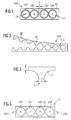
- Figure 1 shows a cross section of an embodiment of a optical ribbon cable LWB, which in this example has four optical fibers LW1 to LW4 has.
- the fiber optic cable LW1 to LW4 have a longitudinal direction along their optical Axis OA on.
- the optical fibers LW1 to LW4 can for example as optical fibers or as optical cables with several optical fibers arranged therein.
- the optical fibers LW1 to LW4 are in their longitudinal directions arranged side by side so that they are parallel to each other come to lie in a common plane.
- the optical fibers LW1 to LW4 are with a first Layer material FC coated, which in this example for Marking of the optical fibers LW1 to LW4 serves.
- the first layer material FC is therefore also called a so-called Called color coating.
- FC Called color coating
- the ribbon cable LWB also has a gap S between the optical fibers LW2 and LW3. This gap S or the space in the vicinity of the gap S is not occupied by optical fibers.
- the gap S can arise, for example, in that the diameters of the optical waveguides LW2 and LW3 deviate from a nominal diameter.
- a nominal diameter of the optical waveguide LW1 to LW4 is, for example, 260 ⁇ m, such a tolerance range, in practice, typically 5 ⁇ m. If the optical ribbon cable LWB has, for example, 12 optical fibers, this can result in a total tolerance range of 60 ⁇ m .
- the optical fibers LW1 to LW4 are also with one second layer material BC coated that the ribbon cable LWF completely surrounds.
- the second layer material is BC also known as so-called band coating.
- the gaps between two adjacent optical fibers filled like the gap S with the band coating BC.
- FIG. 2 shows a schematic illustration in which the upper part of the band coating BC is removed towards the top.
- the second layer material BC which forms the band coating, has a tensile module E and a push module G.
- the force F In order to detach the band coating BC from the color coating FC, the force F must be greater than the adhesive force between the band coating BC and the color coating FC.
- A denotes a cross-sectional area that is related to the layer thickness of the band coating BC.
- FIG. 3 shows a section of the band coating BC from FIG. 2.
- the gap S has a gap width sb.
- the band coating BC has a smallest layer thickness D, which is measured between a horizontal tangent of one of the optical fibers LW1 to LW4 and the outer boundary of the band coating BC.
- the Production of the ribbon cable LWB the location at least one of the Optical waveguide LW2 or LW3 from Figure 1 within the Strip line LWB depending on the layer thickness D of the strip coating BC must be controlled so that there is a gap width sb results according to the above conditions.
- the gap width sb must fall below a value that according to the simplified above relationship depending on the Layer thickness D is.
- Gap width sb also depends on the tension module E and Thrust module G.
- the position In order to meet the required gap width sb, the position must be at least one of the Optical waveguide LW2 or LW3 from Figure 1 within the Ribbon cable LWB also depending on the train module E and of the thrust module G of the band coating BC can be controlled.
- the Gap width sb must have the value according to the above not fall below simplified relationship. According to this Relationship, the value for the gap width sb depends on the tensile modulus E and shear modulus G and the layer thickness D of the Band coatings BC.
- FIG. 4 shows a functional diagram of an exemplary production plant for the production of a ribbon cable LWB.
- the optical fibers LW1 to LW4 are wound on spools SP1 to SP4 provided.
- the optical fibers LW1 to LW4 in a parallel arrangement in the longitudinal direction next to each other, as shown in Figure 1, a coating device BE fed.
- the optical fibers LW1 to LW4 are already coated with the color layer FC according to FIG. 1.
- the container CB contains the matrix material, with the optical fibers LW1 to LW4 in a further operation be coated.
- the contained in the container CB Matrix material forms the later band coating according to BC Figure 1.
- the side-by-side optical waveguide LW1 to LW4 are in the coating device BE with the im Containers CB coated matrix material so that the strip line LWB formed from it completely with the strip coating BC is surrounded.
- the LWB ribbon line is operated by Extraction device RA by the coating device BE drawn.
- the width of the gap is in the measuring device ME S measured.
- the LWB ribbon line is finally on the Drum AT wound up.
- a light source is provided, as in DE 197 02 106 A1 described.
- the ribbon cable LWB is through the light source fully illuminated.
- the light source is, for example, a light diode array intended. If there is a gap S in the strip line LWB, see above a light signal passes through this gap S and arrives to a corresponding element of the diode array.
- the Gap width sb is in relation to the above relationship checked for layer thickness D. When the relationship is violated a signal is derived, which is an adjustment process in the coating device BE depending on the Layer thickness D triggers, so that the gap width sb changes and the relationship is fulfilled.
- the position of the optical fibers LW1 to LW4 within the The strip line LWB can, as also described in DE 197 02 106 A1, by changing the geometric dimensions of the Passage opening DO is influenced in the coating device BE become.
- the optical fibers LW1 to LW4 are thereby through the passage opening DO in its longitudinal direction passed through.
- Width of the passage opening DO made. This is for example one of the two side walls of the passage opening DO designed to be flexible.
- FIG 5 is a cross section of an exemplary passage opening DO shown.
- the optical fibers LW1 to LW4 are in their longitudinal direction through the passage opening DO passed through and coated with the second layer material BC, that forms the band coating.
- the side walls DW1 and / or DW2 are movable. The sidewalls can result from a signal from the measuring device ME readjusted according to Figure 4.
- Such an adjustment process is advantageous at the beginning a manufacturing process for the production of the ribbon cable LWF made and for the production of a batch of Maintain LWB ribbon cables.
- Optical fibers are usually fluctuations in diameter relatively low or the tolerances relatively uniform, so in general it is not necessary continuously readjusted within a batch.
Landscapes
- Physics & Mathematics (AREA)
- Engineering & Computer Science (AREA)
- Manufacturing & Machinery (AREA)
- General Physics & Mathematics (AREA)
- Optics & Photonics (AREA)
- Optical Fibers, Optical Fiber Cores, And Optical Fiber Bundles (AREA)
- Surface Treatment Of Glass Fibres Or Filaments (AREA)
Abstract
Description
- Figur 1
- einen Querschnitt einer Ausführungsform einer optischen Bandleitung mit mehreren Lichtwellenleitern,
- Figur 2
- eine schematische Darstellung der Bandleitung beim Abziehen der umgebenden zweiten Schicht,
- Figur 3
- einen Ausschnitt der umgebenden zweiten Schicht,
- Figur 4
- ein Funktionsbild einer beispielhaften Produktionsanlage,
- Figur 5
- einen Querschnitt einer Durchtrittsöffnung der Beschichtungseinrichtung gemäß Figur 4.
Claims (9)
- Verfahren zur Herstellung einer optischen Bandleitung aus mehreren Lichtwellenleitern mit den Merkmalen:dadurch gekennzeichnet, daßder äußere Umfang mindestens eines Lichtwellenleiters (LW2) wird mit einem ersten Schichtmaterial (FC) beschichtet,der Lichtwellenleiter (LW2) und mindestens ein weiterer Lichtwellenleiter (LW3) werden in deren Längsrichtung (OA) nebeneinander angeordnet und zu einer Bandleitung (LWB) geformt, so daß ein nicht durch Lichtwellenleiter belegter Spalt (S) zwischen den zwei nebeneinander liegenden Lichtwellenleitern (LW2, LW3) entsteht,die Lichtwellenleiter (LW2, LW3) werden mit einem zweiten Schichtmaterial (BC) beschichtet, so daß die Bandleitung (LWB) mit dem zweiten Schichtmaterial (BC) umgeben ist und ein Zwischenraum zwischen den Lichtwellenleitern (LW2, LW3) mit dem zweiten Schichtmaterial (BC) gefüllt ist,
die Lage mindestens eines der Lichtwellenleiter (LW2, LW3) innerhalb der Bandleitung (LWB) in Abhängigkeit einer Schichtdicke (D) des zweiten Schichtmaterials (BC) gesteuert wird. - Verfahren nach Anspruch 1,
dadurch gekennzeichnet, daß
die Lage mindestens eines der Lichtwellenleiter (LW2, LW3) innerhalb der Bandleitung (LWB) so gesteuert wird, daß die Spaltbreite (sb) einen Wert unterschreitet, der abhängig von der Schichtdicke (D) ist. - Verfahren nach Anspruch 1 oder 2,
dadurch gekennzeichnet, daß
die Lage mindestens eines der Lichtwellenleiter (LW2, LW3) innerhalb der Bandleitung (LWB) außerdem in Abhängigkeit eines Zugmoduls (E) und Schubmoduls (G) des zweiten Schichtmaterials (BC) gesteuert wird. - Verfahren nach Anspruch 3,
dadurch gekennzeichnet, daß
die Lage mindestens eines der Lichtwellenleiter (LW2, LW3) innerhalb der Bandleitung (LWB) so gesteuert wird, daß die Spaltbreite (sb) einen Wert unterschreitet, der abhängig von dem Zugmodul (E) und Schubmodul (G) des zweiten Schichtmaterials (BC) ist. - Verfahren nach einem der Ansprüche 1 bis 4,
dadurch gekennzeichnet, daß
die Lage mindestens eines der Lichtwellenleiter (LW2, LW3) innerhalb der Bandleitung (LWB) in Abhängigkeit einer kleinsten auftretenden Schichtdicke (D) des zweiten Schichtmaterials (BC) gesteuert wird. - Verfahren nach einem der Ansprüche 1 bis 5,
dadurch gekennzeichnet, daß
das erste Schichtmaterial (FC) vor dem Aufbringen des zweiten Schichtmaterials (BC) ausgehärtet wird. - Verfahren nach Anspruch 6,
dadurch gekennzeichnet, daß
das erste Schichtmaterial (FC) in einer Atmosphäre mit einem Sauerstoffanteil von 1 bis 250 Partikel per Million Partikel ausgehärtet wird. - Verfahren nach einem der Ansprüche 1 bis 7,
dadurch gekennzeichnet, daß
der Lichtwellenleiter (LW2) mit dem ersten Schichtmaterial (FC) beschichtet wird, so daß sich eine Schichtdicke des ersten Schichtmaterials (FC) zwischen 6 und 9 Mikrometern ergibt. - Verfahren nach einem der Ansprüche 1 bis 8,
dadurch gekennzeichnet, daß
das erste Schichtmaterial (FC) und/oder zweite Schichtmaterial (BC) so gewählt wird, daß die Reißfestigkeit des zweiten Schichtmaterials (BC) größer ist als die Haftkraft zwischen dem ersten Schichtmaterial (FC) und dem zweiten Schichtmaterial (BC).
Applications Claiming Priority (2)
| Application Number | Priority Date | Filing Date | Title |
|---|---|---|---|
| DE10024837 | 2000-05-19 | ||
| DE10024837A DE10024837A1 (de) | 2000-05-19 | 2000-05-19 | Verfahren zur Herstellung einer optischen Bandleitung aus mehreren Lichtwellenleitern |
Publications (2)
| Publication Number | Publication Date |
|---|---|
| EP1156352A1 true EP1156352A1 (de) | 2001-11-21 |
| EP1156352B1 EP1156352B1 (de) | 2003-09-03 |
Family
ID=7642802
Family Applications (1)
| Application Number | Title | Priority Date | Filing Date |
|---|---|---|---|
| EP01109949A Expired - Lifetime EP1156352B1 (de) | 2000-05-19 | 2001-04-24 | Verfahren zur Herstellung einer optischen Bandleitung aus mehreren Lichtwellenleitern |
Country Status (3)
| Country | Link |
|---|---|
| US (1) | US6565685B2 (de) |
| EP (1) | EP1156352B1 (de) |
| DE (2) | DE10024837A1 (de) |
Families Citing this family (2)
| Publication number | Priority date | Publication date | Assignee | Title |
|---|---|---|---|---|
| JP2008090040A (ja) * | 2006-10-03 | 2008-04-17 | Furukawa Electric Co Ltd:The | 光ファイバテープ心線 |
| US20160213200A1 (en) * | 2015-01-26 | 2016-07-28 | Paul Brown | Combination knife and cutting board |
Citations (4)
| Publication number | Priority date | Publication date | Assignee | Title |
|---|---|---|---|---|
| US4720165A (en) * | 1985-02-25 | 1988-01-19 | Mitsubishi Rayon Company Ltd. | Optical fiber sheet and method and apparatus for fabrication thereof |
| EP0262340A2 (de) * | 1986-08-05 | 1988-04-06 | Sumitomo Electric Industries Limited | Optisches Bandkabel mit mehreren Elementen |
| DE19702106A1 (de) * | 1996-04-11 | 1997-10-16 | Siemens Ag | Verfahren und Vorrichtung zur Herstellung einer optischen Bandleitung |
| EP0950908A2 (de) * | 1998-04-17 | 1999-10-20 | Alcatel | Faseroptisches Mehrfachband und Verfahren zu dessen Herstellung |
Family Cites Families (12)
| Publication number | Priority date | Publication date | Assignee | Title |
|---|---|---|---|---|
| US4472021A (en) | 1982-12-10 | 1984-09-18 | Desoto, Inc. | Strippable radiation-cured coatings for optical fiber and method |
| JPS60151257A (ja) | 1984-01-13 | 1985-08-09 | Sumitomo Electric Ind Ltd | 光フアイバ−の製造方法 |
| DE3526823A1 (de) | 1985-07-26 | 1987-02-05 | Siemens Ag | Element mit mehreren lichtwellenleitern |
| CA1307144C (en) | 1987-06-03 | 1992-09-08 | Akira Nishimura | Coated optical fiber tape |
| US4900126A (en) | 1988-06-30 | 1990-02-13 | American Telephone & Telegraph Co. | Bonded array of transmission media |
| DE3829428A1 (de) * | 1988-08-31 | 1990-03-01 | Philips Patentverwaltung | Verfahren zur herstellung eines lichtwellenleiter-flachbandes |
| JPH04268521A (ja) | 1991-02-25 | 1992-09-24 | Sumitomo Electric Ind Ltd | 光ファイバ着色心線の製造方法 |
| DE4126860A1 (de) * | 1991-08-14 | 1993-02-18 | Bayer Ag | Herstellung von lichtleitbaendern |
| JPH06258557A (ja) * | 1993-03-04 | 1994-09-16 | Sumitomo Electric Ind Ltd | 被覆光ファイバユニット |
| CA2129397C (en) * | 1993-12-21 | 2005-03-22 | Mujibar M. Rahman | Process for manufacturing optical fiber ribbons |
| US5485539A (en) * | 1994-08-01 | 1996-01-16 | Siecor Corporation | Fiber optic ribbon cable subunit bearing printed information |
| US5717805A (en) * | 1996-06-12 | 1998-02-10 | Alcatel Na Cable Systems, Inc. | Stress concentrations in an optical fiber ribbon to facilitate separation of ribbon matrix material |
-
2000
- 2000-05-19 DE DE10024837A patent/DE10024837A1/de not_active Withdrawn
-
2001
- 2001-04-24 DE DE50100571T patent/DE50100571D1/de not_active Expired - Fee Related
- 2001-04-24 EP EP01109949A patent/EP1156352B1/de not_active Expired - Lifetime
- 2001-05-17 US US09/860,050 patent/US6565685B2/en not_active Expired - Lifetime
Patent Citations (4)
| Publication number | Priority date | Publication date | Assignee | Title |
|---|---|---|---|---|
| US4720165A (en) * | 1985-02-25 | 1988-01-19 | Mitsubishi Rayon Company Ltd. | Optical fiber sheet and method and apparatus for fabrication thereof |
| EP0262340A2 (de) * | 1986-08-05 | 1988-04-06 | Sumitomo Electric Industries Limited | Optisches Bandkabel mit mehreren Elementen |
| DE19702106A1 (de) * | 1996-04-11 | 1997-10-16 | Siemens Ag | Verfahren und Vorrichtung zur Herstellung einer optischen Bandleitung |
| EP0950908A2 (de) * | 1998-04-17 | 1999-10-20 | Alcatel | Faseroptisches Mehrfachband und Verfahren zu dessen Herstellung |
Also Published As
| Publication number | Publication date |
|---|---|
| EP1156352B1 (de) | 2003-09-03 |
| DE10024837A1 (de) | 2001-11-22 |
| DE50100571D1 (de) | 2003-10-09 |
| US20020007916A1 (en) | 2002-01-24 |
| US6565685B2 (en) | 2003-05-20 |
Similar Documents
| Publication | Publication Date | Title |
|---|---|---|
| DE2424041C2 (de) | Faseroptisches Band und Verfahren zu seiner Herstellung | |
| DE69614382T2 (de) | Faseroptisches bandkabel und verfahren zur dessen herstellung | |
| DE69921539T2 (de) | Geschlitztes Kompositkabel mit einem Kabelprofil mit einer rohrförmiger Öffnung für Kupferpaare und ein Schlitz für einen optischen Faser | |
| DE68914349T2 (de) | Methode zur Herstellung eines optischen Verzweigungs- und Kopplungselements. | |
| DE60101402T2 (de) | Randverklebte aber teilbare faseroptische Bandkabel | |
| EP0736194A1 (de) | Optische faser mit einer farbkennzeichnung | |
| DE19711121B4 (de) | Verzweigende Lichtwellenleiteranordnung und verzweigendes Lichtwellenleiterarray | |
| EP0127042A2 (de) | Optisches Kabel | |
| EP1730567A1 (de) | Mechanisch auftrennbares kabel | |
| DE2701650C2 (de) | Ader für ein optisches Kabel bzw. ein optisches Kabelelement | |
| DE19826301A1 (de) | Optische Faser und Verfahren zum Kennzeichnen einer optischen Faser | |
| EP0135224A2 (de) | Verfahren zur Herstellung von Kabeln sowie nach diesem Verfahren hergestellte Kabel, insbesondere optische Kabel | |
| EP1156352B1 (de) | Verfahren zur Herstellung einer optischen Bandleitung aus mehreren Lichtwellenleitern | |
| EP0258839A2 (de) | Optisches Kabel und Verfahren zu dessen Herstellung | |
| DE2830623A1 (de) | Lichtuebertragungskabel und verfahren zu seiner herstellung | |
| DE3526823A1 (de) | Element mit mehreren lichtwellenleitern | |
| DE2849501C2 (de) | ||
| DE69430756T2 (de) | Faseroptischer koppler | |
| DE69804691T2 (de) | Faseroptisches Kabel | |
| EP0416207B1 (de) | Lichtwellenleiterkabel | |
| DE4214039C2 (de) | Vorrichtung zum Aufteilen von Lichtwellenleitern eines optischen Kabels | |
| DE19931944B4 (de) | Umlenkende Auskopplung in einer Leiterplatte eingebetteter Lichtleiter | |
| DE3411595C2 (de) | ||
| EP0363853A1 (de) | Verfahren zur Herstellung eines faseroptischen Sternkopplers und nach diesem Verfahren hergestellter faseroptischer Sternkoppler | |
| DE4211489A1 (de) | Optisches Übertragungselement |
Legal Events
| Date | Code | Title | Description |
|---|---|---|---|
| PUAI | Public reference made under article 153(3) epc to a published international application that has entered the european phase |
Free format text: ORIGINAL CODE: 0009012 |
|
| AK | Designated contracting states |
Kind code of ref document: A1 Designated state(s): AT BE CH CY DE DK ES FI FR GB GR IE IT LI LU MC NL PT SE TR Kind code of ref document: A1 Designated state(s): DE FR GB |
|
| AX | Request for extension of the european patent |
Free format text: AL;LT;LV;MK;RO;SI |
|
| 17P | Request for examination filed |
Effective date: 20011214 |
|
| 17Q | First examination report despatched |
Effective date: 20020326 |
|
| AKX | Designation fees paid |
Free format text: DE FR GB |
|
| GRAH | Despatch of communication of intention to grant a patent |
Free format text: ORIGINAL CODE: EPIDOS IGRA |
|
| GRAH | Despatch of communication of intention to grant a patent |
Free format text: ORIGINAL CODE: EPIDOS IGRA |
|
| GRAA | (expected) grant |
Free format text: ORIGINAL CODE: 0009210 |
|
| RAP1 | Party data changed (applicant data changed or rights of an application transferred) |
Owner name: CCS TECHNOLOGY, INC. |
|
| AK | Designated contracting states |
Kind code of ref document: B1 Designated state(s): DE FR GB |
|
| PG25 | Lapsed in a contracting state [announced via postgrant information from national office to epo] |
Ref country code: GB Free format text: LAPSE BECAUSE OF FAILURE TO SUBMIT A TRANSLATION OF THE DESCRIPTION OR TO PAY THE FEE WITHIN THE PRESCRIBED TIME-LIMIT Effective date: 20030903 |
|
| REG | Reference to a national code |
Ref country code: GB Ref legal event code: FG4D Free format text: NOT ENGLISH |
|
| REF | Corresponds to: |
Ref document number: 50100571 Country of ref document: DE Date of ref document: 20031009 Kind code of ref document: P |
|
| GBV | Gb: ep patent (uk) treated as always having been void in accordance with gb section 77(7)/1977 [no translation filed] |
Effective date: 20030903 |
|
| ET | Fr: translation filed | ||
| PLBE | No opposition filed within time limit |
Free format text: ORIGINAL CODE: 0009261 |
|
| STAA | Information on the status of an ep patent application or granted ep patent |
Free format text: STATUS: NO OPPOSITION FILED WITHIN TIME LIMIT |
|
| 26N | No opposition filed |
Effective date: 20040604 |
|
| PGFP | Annual fee paid to national office [announced via postgrant information from national office to epo] |
Ref country code: FR Payment date: 20050418 Year of fee payment: 5 |
|
| PGFP | Annual fee paid to national office [announced via postgrant information from national office to epo] |
Ref country code: DE Payment date: 20050531 Year of fee payment: 5 |
|
| PG25 | Lapsed in a contracting state [announced via postgrant information from national office to epo] |
Ref country code: DE Free format text: LAPSE BECAUSE OF NON-PAYMENT OF DUE FEES Effective date: 20061101 |
|
| REG | Reference to a national code |
Ref country code: FR Ref legal event code: ST Effective date: 20061230 |
|
| PG25 | Lapsed in a contracting state [announced via postgrant information from national office to epo] |
Ref country code: FR Free format text: LAPSE BECAUSE OF NON-PAYMENT OF DUE FEES Effective date: 20060502 |