EP1154486A1 - ESD-Schutzstruktur mit parallelen Bipolartransistoren - Google Patents
ESD-Schutzstruktur mit parallelen Bipolartransistoren Download PDFInfo
- Publication number
- EP1154486A1 EP1154486A1 EP01111009A EP01111009A EP1154486A1 EP 1154486 A1 EP1154486 A1 EP 1154486A1 EP 01111009 A EP01111009 A EP 01111009A EP 01111009 A EP01111009 A EP 01111009A EP 1154486 A1 EP1154486 A1 EP 1154486A1
- Authority
- EP
- European Patent Office
- Prior art keywords
- zones
- protective structure
- emitter
- structure according
- esd protective
- Prior art date
- Legal status (The legal status is an assumption and is not a legal conclusion. Google has not performed a legal analysis and makes no representation as to the accuracy of the status listed.)
- Granted
Links
- 239000004065 semiconductor Substances 0.000 claims abstract description 36
- 238000011144 upstream manufacturing Methods 0.000 claims abstract 2
- 230000001681 protective effect Effects 0.000 claims description 50
- 239000002800 charge carrier Substances 0.000 claims description 6
- 239000004020 conductor Substances 0.000 claims description 6
- 239000000758 substrate Substances 0.000 description 11
- 230000015556 catabolic process Effects 0.000 description 9
- 238000001465 metallisation Methods 0.000 description 9
- 238000009792 diffusion process Methods 0.000 description 7
- 230000006378 damage Effects 0.000 description 6
- 238000000034 method Methods 0.000 description 6
- 230000003071 parasitic effect Effects 0.000 description 5
- 239000000969 carrier Substances 0.000 description 4
- 238000004519 manufacturing process Methods 0.000 description 4
- 238000009826 distribution Methods 0.000 description 3
- 230000000694 effects Effects 0.000 description 3
- 238000002513 implantation Methods 0.000 description 3
- 238000005468 ion implantation Methods 0.000 description 3
- 230000000903 blocking effect Effects 0.000 description 2
- 238000011161 development Methods 0.000 description 2
- 230000018109 developmental process Effects 0.000 description 2
- 238000005516 engineering process Methods 0.000 description 2
- 238000000265 homogenisation Methods 0.000 description 2
- 230000036961 partial effect Effects 0.000 description 2
- 230000002829 reductive effect Effects 0.000 description 2
- 230000002441 reversible effect Effects 0.000 description 2
- XUIMIQQOPSSXEZ-UHFFFAOYSA-N Silicon Chemical compound [Si] XUIMIQQOPSSXEZ-UHFFFAOYSA-N 0.000 description 1
- 230000004888 barrier function Effects 0.000 description 1
- 238000002485 combustion reaction Methods 0.000 description 1
- 230000001419 dependent effect Effects 0.000 description 1
- 238000010586 diagram Methods 0.000 description 1
- 238000005530 etching Methods 0.000 description 1
- 238000010304 firing Methods 0.000 description 1
- 238000003780 insertion Methods 0.000 description 1
- 230000037431 insertion Effects 0.000 description 1
- 230000000670 limiting effect Effects 0.000 description 1
- 238000012986 modification Methods 0.000 description 1
- 230000004048 modification Effects 0.000 description 1
- 229910021420 polycrystalline silicon Inorganic materials 0.000 description 1
- 229920005591 polysilicon Polymers 0.000 description 1
- 238000004886 process control Methods 0.000 description 1
- 230000000717 retained effect Effects 0.000 description 1
- 229910052710 silicon Inorganic materials 0.000 description 1
- 239000010703 silicon Substances 0.000 description 1
- 238000012549 training Methods 0.000 description 1
Images


Classifications
-
- H—ELECTRICITY
- H10—SEMICONDUCTOR DEVICES; ELECTRIC SOLID-STATE DEVICES NOT OTHERWISE PROVIDED FOR
- H10D—INORGANIC ELECTRIC SEMICONDUCTOR DEVICES
- H10D89/00—Aspects of integrated devices not covered by groups H10D84/00 - H10D88/00
- H10D89/60—Integrated devices comprising arrangements for electrical or thermal protection, e.g. protection circuits against electrostatic discharge [ESD]
- H10D89/601—Integrated devices comprising arrangements for electrical or thermal protection, e.g. protection circuits against electrostatic discharge [ESD] for devices having insulated gate electrodes, e.g. for IGFETs or IGBTs
- H10D89/711—Integrated devices comprising arrangements for electrical or thermal protection, e.g. protection circuits against electrostatic discharge [ESD] for devices having insulated gate electrodes, e.g. for IGFETs or IGBTs using bipolar transistors as protective elements
-
- H—ELECTRICITY
- H10—SEMICONDUCTOR DEVICES; ELECTRIC SOLID-STATE DEVICES NOT OTHERWISE PROVIDED FOR
- H10D—INORGANIC ELECTRIC SEMICONDUCTOR DEVICES
- H10D89/00—Aspects of integrated devices not covered by groups H10D84/00 - H10D88/00
- H10D89/60—Integrated devices comprising arrangements for electrical or thermal protection, e.g. protection circuits against electrostatic discharge [ESD]
- H10D89/601—Integrated devices comprising arrangements for electrical or thermal protection, e.g. protection circuits against electrostatic discharge [ESD] for devices having insulated gate electrodes, e.g. for IGFETs or IGBTs
- H10D89/811—Integrated devices comprising arrangements for electrical or thermal protection, e.g. protection circuits against electrostatic discharge [ESD] for devices having insulated gate electrodes, e.g. for IGFETs or IGBTs using FETs as protective elements
Definitions
- the invention relates to an ESD protective structure for protecting an Integrated semiconductor circuit against electrostatic discharge.
- ESD protective structures for protection against electrostatic overvoltages.
- These ESD protective structures can be used as clamping circuits between the supply voltage lines of the integrated Circuit can be inserted and in the case of an electrostatic Discharge the parasitic voltage on one of the supply voltage lines deduce. In this way, the parasitic Overvoltage between the supply voltage lines acceptable values are reduced.
- ESD protective structures are at least partially blocking Semiconductor components, such as thyristors, diodes or bipolar transistors used.
- ESD diodes have the disadvantage that at very high The voltage drop across the diode sometimes flows as large can be sensitive components of the to be protected Circuit, for example their gate oxides or diffusion areas, be irreversibly damaged. In addition, the power consumption the diode is very large in reverse operation.
- ESD protective structures are therefore often used uses a variety of parallel, have bipolar field oxide transistors as ESD protection.
- These ESD protective structures which are particularly good for Suitable for limiting parasitic overvoltages, show reverse bias in the characteristic curve is initially a blocking Behavior until a first voltage breakdown is reached in which the current-voltage characteristic curve to a lower Tension as the breakdown voltage snaps back. This snap back to the lower, so-called holding voltage also known as snap-back behavior.
- the current-voltage characteristic curve essentially has a holding voltage a linear slope until it leads to a second voltage breakdown reached, in which the ESD protective structure destroyed and which must therefore be avoided at all costs.
- the Many of the ESD transistors arranged in parallel should therefore with a coupled overvoltage pulse if possible switch through simultaneously and evenly.
- the present invention is therefore based on the object to provide an ESD protection structure that is one possible uniform switching on of the transistors of the ESD protection structure guaranteed.
- the ESD protection structure has a single common rail resistance that drives each bipolar transistor.
- This Path resistance is advantageously through in the semiconductor body introduced deep implantation area or diffusion area generated. These deep doping areas work like an artificially enlarged distance or a barrier between the base zone and the area where the collector zones and the emitter zones are arranged. Thus, carriers become artificially prevented from diffusing directly to the base zones, but need a detour into the depth of the substrate to take.
- the ones that arise during a first voltage breakdown As a result, load carriers are predominantly in an area below of the emitter zones and collector zones retained what significantly favors a subsequent ignition process. Thereby, that is in the area below the collector and Emitter always a defined and essentially equally distributed Amount of carriers located can be even and rapid firing of the bipolar transistors of the ESD protective structure be guaranteed.
- the trough-shaped areas in each case at the outermost zones of the first line type, for Example the outer emitter zones, are connected and the same Line type such as these have (emitter) zones.
- the trough-shaped areas are then at the same potential as the (emitter) zones, which ensures that the charge carriers a much larger path through the substrate of the Semiconductor body must go back to the base zones reach.
- the trough-shaped areas a significantly lower doping concentration than that connected (emitter) zones. It would also be conceivable - albeit not so advantageous - if the trough-shaped areas are undoped or contain a dielectric.
- the trough-shaped areas protrude much deeper into the semiconductor body than that (Emitter) zones to which they adjoin or are connected are.
- the trough-shaped areas can pass through a deep implantation, for example by a multiple ion implantation, or by diffusion followed by deep driving step.
- a common trench etching process and filling with doped or undoped polysilicon or with a dielectric are also advantageous.
- the emitter zones and the collector zones laterally enclosed by the base zones and the trough-shaped areas, which provides better latch-up protection for the ESD protective structure is guaranteed.
- This latch-up protection can be further improved by all zones of the ESD structure - that means the emitter zones, the collector zones, the Base zones and the trough-shaped areas - in an additional one Trough are embedded and thus separated from the substrate potential are.
- the Emitter zones and collector zones are strip-shaped.
- the strip-shaped collector zones and emitter zones are then parallel arranged side by side, with collector zones and Alternate emitter zones.
- This arrangement essentially has the ESD protective structure square layout, creating a significant homogenization the current of the ESD structure is guaranteed. A further homogenization of the stream can thereby be achieved that the emitter zones and collector zones of the respective Electrodes are continuously contacted.
- the strip-shaped emitter electrodes and the collector electrodes with the conductor track to which they are connected respectively form a finger-like structure that then intertwines are. This ensures that the greatest current densities and thus the greatest voltage drops opposite sides of the respective conductor tracks arise, resulting in burns caused by voltage breakdowns on the conductor tracks can be significantly reduced.
- the ESD protective structure according to the invention is particularly suitable in bipolar transistors designed as field oxide transistors.
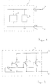
- Fig. 1 shows a circuit arrangement with an inventive ESD protective structure.
- 1 is the integrated Semiconductor circuit called.
- the semiconductor integrated circuit 1 is through its two supply voltage inputs 2, 3 with a first potential rail 4 with a first supply potential VCC and a second potential rail 5 with a second supply potential VSS that in the present Example is the potential of the reference ground.
- the semiconductor integrated circuit 1 also assigns one protective circuit 6, for example a logic circuit, a program-controlled unit, a semiconductor memory, a Power circuit, etc., on. Furthermore, the integrated Semiconductor circuit 1 has an ESD protection structure 7 for protecting the circuit 6 to be protected.
- the circuit to be protected 6 and the ESD protective structure 7 are each between the potential rails 4, 5 switched.
- Fig. 2 shows a circuit arrangement of the shown in Fig. 1, ESD protective structure according to the invention.
- the ESD protection structure 7 has three bipolar field oxide transistors T1, T2, T3.
- the Bipolar transistors T1 - T3 are parallel across their load paths arranged and connected between the potential rails 4, 5, where in the present embodiment, the respective Emitter connections E with the potential of the reference ground VSS and the respective collector connections C with the supply potential VCC are connected.
- the basic connections are according to the invention B of the bipolar transistors T1 - T3 short-circuited to one another and via a rail resistance RB to the reference potential VSS and thus the emitter connections E coupled.
- Fig. 3 shows in a partial section that shown in Fig. 2 ESD protective structure.
- 10 is a section of a Semiconductor body called.
- the semiconductor body 10 is made in the present exemplary embodiment from weakly p-doped silicon substrate.
- the semiconductor body 10 has a pane front 11, in the first and second n-doped regions 12, 13 are embedded.
- the first n-doped regions 12 are the collector zones in the present exemplary embodiment
- the second n-doped regions 13 are the emitter zones.
- Collector zones 12 and emitter zones 13 are on the surface 11 arranged alternately and from each other by a substrate zone 10 'or a field oxide 14 spaced apart.
- p-doped Areas 15, which form the base zones here, in the Semiconductor body 10 embedded. Enclose these base zones 15 the collector zones 12 and emitter zones 13 and are of these for example also spaced apart by a field oxide 16.
- the collector zones 12, the emitter zones 13 and the base zones 14 are on the surface 11 of the semiconductor body 10, respectively contacted via contact electrodes 18, 19, 20.
- the collector electrodes 18 are shorted together and with the first supply potential VCC connected.
- the emitter electrodes 19 and the base electrodes 20 are also together short-circuited and connected to the potential of the reference ground VSS.
- the outer emitter zones 13 - trough-shaped areas 17 are between the base zones 15 and the outer n-doped regions 12, 13 - in the present exemplary embodiment these are the outer emitter zones 13 - trough-shaped areas 17 introduced into the semiconductor body 10, which to the outer emitter zones 13 are connected.
- the tub-shaped Areas 17 have the same conduction type here, but a smaller one Doping concentration than the emitter zones 13, however, they could also be undoped or contain a dielectric.
- the areas 17 do not necessarily have to be trough-shaped, but can be in the frame to manufacture the respective semiconductor integrated circuit technology also used differently, for example be trench-shaped.
- the lateral and / or vertical dimensions of the trough-shaped regions 17 shaped in this way are that the effective drift distance of charge carriers between the p-doped base zones 15 and the substrate zones 10 'in the semiconductor substrate 10 is significantly extended.
- the areas 17 significantly deeper in the Semiconductor body 10 has been introduced as the corresponding Emitter zones 13 and / or collector zones 12.
- the mode of operation of the ESD protection structure according to the invention is described below 7 described in more detail.
- the weakly n-doped trough-shaped areas 17 are according to the invention with the outer n-doped emitter zones 13 are fused and thus also have their potential, that is to say the reference potential VSS.
- This trough-shaped areas 17, depending on the technology process used through a high energy ion implantation or a deep diffusion can be created, which prevent charge carrier arising from a first voltage breakdown rapid diffusion into the substrate and thus into the base zones, because the effective way to use them as substrate contact Base zones 15 clearly through the trough-shaped area 17 is extended.
- FIG. 4 shows a top view of an advantageous layout of a ESD protective structure 7 according to FIG. 2.
- the entire ESD protective structure 7 here has an essentially square one Layout on top that has an even power distribution favored on the various bipolar transistors T1-T3. Due to the square layout, in which the emitter zones 13 and the collector zones 12 are strip-shaped and parallel arranged side by side, it ensures that none of the bipolar transistors T1-T3 fundamentally different substrate effects "gets to see” as the adjacent bipolar transistor T1-T3.
- a square Layout prevents the voltage drop of the contact metallization becomes too large and therefore an uneven current distribution, like this for example with a strongly rectangular one Layout would be the case.
- the invention is not exclusively square Layouts of the ESD protective structures 7, but can, although not as advantageous, even with rectangular, round or oval, hexagonal or similar layouts be used.
- the emitter and collector zones 12, 13 not necessarily strip-shaped and can be arranged side by side, but can advantageously also circular, square, meandering, fan-shaped or be arranged similarly. These are advantageously Emitter zones 13, collector zones 12 and base zones 15 through the respective electrodes 18, 19, 20 as far as possible continuously contacted in order to further homogenize the current flow to enable.
- FIG. 5 shows an advantageous arrangement in a top view the conductor tracks for contacting the emitter electrodes and the collector electrodes.
- FIG. 5 shows the two metallizations for the potential rails 4, 5. Furthermore, FIG. 5 shows the strips and juxtaposed emitter electrodes 19 and Collector electrodes 18. These electrodes 18, 19 are finger-shaped Metallizations 18 ', 19' with their respective assigned Potential rail 4, 5 connected. The metallization fingers 18 ', 19' are interleaved and each on the opposing potential rails 4, 5 connected.
- FIGS. 2 to 5 Another embodiment shown in the figures of the drawing not shown, offers the possibility that a ESD protection structure according to FIGS. 2 to 5 next to one another as desired is arranged frequently. It is important to ensure that the p-doped base zones 15 are always arranged outside and the Enclose collector zones 12 and emitter zones 13. Thereby, that the base zones 15 completely enclose the zones 12, 13, the ESD protective structure 7 is defined all around Potential kept, resulting in improved latch-up protection can be guaranteed. However, it would also be conceivable that the base zones 15 do not completely enclose the zones 12, 13, however, such a structure offers a smaller one latch-up protection.
- the ESD protection structure described in the exemplary embodiments has only three bipolar transistors T1 -T3; This ESD protective structure therefore has three emitter fingers in its layout and two collector fingers on. Of course you can the present invention also with more or less bipolar transistors Realize T1-T3.
- the emitters should be as external as possible Exclude parasitic edge effects.
- the base zones 15, collector zones 12 and 12 shown in FIG Emitter zones 13 can be by diffusion or by ion implantation be introduced into the semiconductor body 10, however the doping method used is essentially determined according to the respective manufacturing processes for manufacturing the integrated circuit.
- the ESD protective structure 7 described above avoids the problems of the inhomogeneous current flow mentioned at the beginning accompanying rapid destruction of the ESD protective structure.
- This solution to the problem is almost exclusively with layout means achieved and therefore requires no expensive special processes or special masks. It's just a minor one here Additional expenditure on chip area is required, but this means that Self-protection effect of the described ESD protection structure in considerable Dimensions can be increased.
- the ESD protective structure according to the invention is particularly suitable in MOS / CMOS integrated semiconductor circuits, the one Protection of the supply voltage lines and also the inputs or need outputs.
- MOS / CMOS integrated semiconductor circuits the one Protection of the supply voltage lines and also the inputs or need outputs.
- these are all integrated Circuits with analog and digital functions with their own analog supply voltage, especially such circuits, who work with high operating voltage and therefore none Own protection.
Landscapes
- Semiconductor Integrated Circuits (AREA)
Abstract
Description
- Figur 1
- eine Schaltungsanordnung mit einer erfindungsgemäßen ESD-Schutzstruktur;
- Figur 2
- ein Schaltbild der in Fig. 1 gezeigten erfindungsgemäßen ESD-Schutzstruktur bestehend aus drei Bipolartransistoren;
- Figur 3
- in einem Teilschnitt ein Ausführungsbeispiel der in Fig. 2 gezeigten ESD-Schutzstruktur;
- Figur 4
- in einer Draufsicht ein vorteilhaftes Layout zur Kontaktierung von Emitter, Basis und Kollektor der ESD-Schutzstruktur entsprechend Figur 3;
- Figur 5
- in einer Draufsicht eine vorteilhafte Anordnung der Leiterbahnen zur Kontaktierung der Emitterelektroden und der Kollektorelektroden.
- 1
- integrierte Halbleiterschaltung
- 2
- Versorgungsspannungseingang
- 3
- Versorgungsspannungseingang
- 4
- erste Potentialschiene
- 5
- zweite Potentialschiene
- 6
- zu schützende Schaltung
- 7
- ESD-Schutzstruktur
- 10
- Halbleiterkörper
- 10'
- Bereiche zwischen benachbarten Emitter- und Kollektorzonen, Substratzone
- 10''
- Bereiche unterhalb der Emitter-/Kollektorzonen
- 11
- Oberfläche des Halbleiterkörpers
- 12
- Kollektorzonen
- 13
- Emitterzonen
- 14
- Feldoxid
- 15
- Basiszonen
- 16
- Feldoxid
- 17
- wannenförmige Bereiche
- 18
- Kollektorelektrode
- 18'
- fingerförmige Kollektormetallisierung
- 19
- Emitterelektroden
- 19'
- fingerförmige Emittermetallisierung
- 20
- Basiselektroden
- B
- Basisanschluss
- C
- Kollektoranschluss
- E
- Emitteranschluss
- RB
- (Basis-)Bahnwiderstand
- T1, T2, T3
- Bipolartransistoren
- VCC
- erstes Versorgungspotential
- VSS
- zweites Versorgungspotential, Potential der Bezugsmasse
Claims (12)
- ESD-Schutzstruktur zum Schutz einer zwischen einer ersten Potentialschiene (4) mit einem ersten Versorgungspotential (VCC) und einer zweiten Potentialschiene (5) mit einem zweiten Versorgungspotential (VSS) geschalteten, integrierten Halbleiterschaltung (1) vor elektrostatischer Entladung, mit einer Mehrzahl von lateral ausgebildeten Bipolartransistoren (T1-T3), deren Laststrecken parallel zueinander und zwischen den Potentialschienen (4, 5) angeordnet sind und deren Steueranschlüsse (B) an einer der Potentialschienen (4, 5) angeschlossen ist, wobei ein einziger in den Halbleiterkörper (10) mitintegrierten Bahnwiderstand (RB) vorgesehen ist, der jedem Steueranschluss (B) der Bipolartransistoren (T1 - T3) vorgeschaltet ist.
- ESD-Schutzstruktur nach Anspruch 1,
dadurch gekennzeichnet, dass
ein Halbleiterkörper (10) vorgesehen ist, in den mindestens eine Emitterzone (13) und mindestens eine Kollektorzone (12) des ersten Leitungstyps und mindestens eine Basiszone (15) des zweiten, entgegengesetzten Leitungstyps eingebettet sind, wobei zwischen den Zonen (12, 13) des ersten Leitungstyps und den Basiszonen (15) jeweils ein wannenförmiger Bereich (17) in den Halbleiterkörper (10) eingebracht ist, der die effektive freie Weglänge von Ladungsträgern zu den Basiszone (15) verlängert. - ESD-Schutzstruktur nach Anspruch 2,
dadurch gekennzeichnet, dass
der wannenförmige Bereich (17) jeweils an eine der Zonen (12, 13) des ersten Leitungstyps angeschlossen ist. - ESD-Schutzstruktur nach Anspruch 3,
dadurch gekennzeichnet, dass
der wannenförmige Bereich (17) denselben Leitungstyp wie die diejenige Zone (12, 13), an die er angeschlossen ist, jedoch eine geringere Dotierungskonzentration aufweist. - ESD-Schutzstruktur nach einem der Ansprüche 2 bis 4,
dadurch gekennzeichnet, dass
der wannenförmige Bereich (17) sehr viel tiefer in den Halbleiterkörper (10) hineinragt als diejenige Zone (12, 13), an die er angrenzt oder angeschlossen ist. - ESD-Schutzstruktur nach einem der Ansprüche 2 bis 5,
dadurch gekennzeichnet, dass
die Basiszonen (15) und die wannenförmigen Bereiche (17) die Emitterzonen (13) und die Kollektorzonen (13) lateral umschließen. - ESD-Schutzstruktur nach einem der Ansprüche 2 bis 6,
dadurch gekennzeichnet, dass
der Halbleiterkörper (10) Ladungsträger vom ersten Leitungstyp aufweist und in den Halbleiterkörper (10) mindestens eine weitere Wanne des zweiten Leitungstyps eingebettet ist, in der die Emitterzonen (13), Kollektorzonen (12), Basiszonen (15) und wannenförmigen Bereiche (17) eingebettet sind. - ESD-Schutzstruktur nach einem der Ansprüche 2 bis 7,
dadurch gekennzeichnet, dass
die Emitterzonen (13) und Kollektorzonen (12) streifenförmig derart ausgebildet sind, dass sie abwechselnd nebeneinander und parallel zueinander angeordnet sind. - ESD-Schutzstruktur nach einem der vorstehenden Ansprüche,
dadurch gekennzeichnet, dass
die ESD-Schutzstruktur (7) ein im Wesentlichen quadratisches Layout aufweist. - ESD-Schutzstruktur nach einem der vorstehenden Ansprüche,
dadurch gekennzeichnet, dass
die Emitterzonen (13) von den Emitterelektroden (19) und die Kollektorzonen (12) von den Kollektorelektroden (18) durchgehend kontaktiert sind. - ESD-Schutzstruktur nach einem der vorstehenden Ansprüche,
dadurch gekennzeichnet, dass
die Emitterelektroden (19) und die Kollektorelektroden (18) über Leiterbahnen (19', 18') an jeweils einer gegenüberliegenden Potentialschiene (4, 5) angeschlossen sind und somit fingerförmige Anschlüsse bilden, die ineinander verschränkt sind. - ESD-Schutzstruktur nach einem der vorstehenden Ansprüche,
dadurch gekennzeichnet, dass
die Bipolartransistoren (T1 - T3) als Feldoxidtransisitoren ausgebildet sind.
Applications Claiming Priority (2)
| Application Number | Priority Date | Filing Date | Title |
|---|---|---|---|
| DE10022366A DE10022366A1 (de) | 2000-05-08 | 2000-05-08 | ESD-Schutzstruktur |
| DE10022366 | 2000-05-08 |
Publications (2)
| Publication Number | Publication Date |
|---|---|
| EP1154486A1 true EP1154486A1 (de) | 2001-11-14 |
| EP1154486B1 EP1154486B1 (de) | 2016-02-24 |
Family
ID=7641186
Family Applications (1)
| Application Number | Title | Priority Date | Filing Date |
|---|---|---|---|
| EP01111009.5A Expired - Lifetime EP1154486B1 (de) | 2000-05-08 | 2001-05-08 | ESD-Schutzstruktur mit parallelen Bipolartransitoren |
Country Status (3)
| Country | Link |
|---|---|
| US (1) | US20020003236A1 (de) |
| EP (1) | EP1154486B1 (de) |
| DE (1) | DE10022366A1 (de) |
Families Citing this family (4)
| Publication number | Priority date | Publication date | Assignee | Title |
|---|---|---|---|---|
| TWI505436B (zh) * | 2011-09-15 | 2015-10-21 | Macronix Int Co Ltd | 半導體元件、靜電放電保護元件及其製造方法 |
| US8901649B2 (en) * | 2011-09-21 | 2014-12-02 | Macronix International Co., Ltd. | Semiconductor device, electrostatic discharge protection device and manufacturing method thereof |
| US9324845B2 (en) | 2012-12-11 | 2016-04-26 | Infineon Technologies Ag | ESD protection structure, integrated circuit and semiconductor device |
| US11855074B2 (en) * | 2021-02-08 | 2023-12-26 | Globalfoundries U.S. Inc. | Electrostatic discharge devices |
Citations (4)
| Publication number | Priority date | Publication date | Assignee | Title |
|---|---|---|---|---|
| EP0575062A1 (de) * | 1992-06-05 | 1993-12-22 | AT&T Corp. | ESD-Schutz von Ausgangspuffern |
| EP0851494A2 (de) * | 1996-12-27 | 1998-07-01 | Nec Corporation | Halbleiteranordnung mit einer Schutzschaltung |
| US5898206A (en) * | 1996-12-26 | 1999-04-27 | Nec Corporation | Semiconductor device |
| EP0948051A2 (de) * | 1998-03-24 | 1999-10-06 | Nec Corporation | Halbleiterbauteil mit Schutzschaltung |
Family Cites Families (6)
| Publication number | Priority date | Publication date | Assignee | Title |
|---|---|---|---|---|
| US5043782A (en) * | 1990-05-08 | 1991-08-27 | David Sarnoff Research Center, Inc. | Low voltage triggered snap-back device |
| US5477414A (en) * | 1993-05-03 | 1995-12-19 | Xilinx, Inc. | ESD protection circuit |
| KR100496362B1 (ko) * | 1995-07-11 | 2006-05-02 | 텍사스 인스트루먼츠 인코포레이티드 | 기판트리거된래터럴npn을이용한집적esd보호회로 |
| US5896315A (en) * | 1997-04-11 | 1999-04-20 | Programmable Silicon Solutions | Nonvolatile memory |
| EP0903828A1 (de) * | 1997-09-23 | 1999-03-24 | STMicroelectronics S.r.l. | Verbesserte Vorrichtung zum Schutz einer integrierten Schaltung gegen elektrostatische Entladungen |
| US6075271A (en) * | 1998-03-03 | 2000-06-13 | Motorola, Inc. | Semiconductor device inhibiting parasitic effects during electrostatic discharge |
-
2000
- 2000-05-08 DE DE10022366A patent/DE10022366A1/de not_active Withdrawn
-
2001
- 2001-05-08 EP EP01111009.5A patent/EP1154486B1/de not_active Expired - Lifetime
- 2001-05-08 US US09/852,123 patent/US20020003236A1/en not_active Abandoned
Patent Citations (4)
| Publication number | Priority date | Publication date | Assignee | Title |
|---|---|---|---|---|
| EP0575062A1 (de) * | 1992-06-05 | 1993-12-22 | AT&T Corp. | ESD-Schutz von Ausgangspuffern |
| US5898206A (en) * | 1996-12-26 | 1999-04-27 | Nec Corporation | Semiconductor device |
| EP0851494A2 (de) * | 1996-12-27 | 1998-07-01 | Nec Corporation | Halbleiteranordnung mit einer Schutzschaltung |
| EP0948051A2 (de) * | 1998-03-24 | 1999-10-06 | Nec Corporation | Halbleiterbauteil mit Schutzschaltung |
Also Published As
| Publication number | Publication date |
|---|---|
| EP1154486B1 (de) | 2016-02-24 |
| US20020003236A1 (en) | 2002-01-10 |
| DE10022366A1 (de) | 2001-11-29 |
Similar Documents
| Publication | Publication Date | Title |
|---|---|---|
| EP1019964B1 (de) | Integrierte halbleiterschaltung mit schutzstruktur zum schutz vor elektrostatischer entladung | |
| DE69330455T2 (de) | Überspannungsschutzstruktur für vertikale Halbleiterkomponenten | |
| DE3856420T2 (de) | Gegen elektrostatische Entladungen geschützter integrierter Schaltkreis mit variablem Schutzschwellwert | |
| DE19651247C2 (de) | Eingabe/Ausgabeschutzschaltung | |
| DE2559360A1 (de) | Halbleiterbauteil mit integrierten schaltkreisen | |
| DE19654163B4 (de) | Schutzvorrichtung für eine Halbleiterschaltung | |
| DE2348643A1 (de) | Integrierte schutzschaltung fuer einen hauptschaltkreis aus feldeffekttransistoren | |
| DE4120394A1 (de) | Monolithisch integrierte schaltungsanordnung | |
| DE19528998C2 (de) | Bidirektionaler Halbleiterschalter und Verfahren zu seiner Steuerung | |
| DE60318196T2 (de) | Halbleiteranordnungen mit graben-gate | |
| DE1216435B (de) | Schaltbares Halbleiterbauelement mit vier Zonen | |
| DE10148794B4 (de) | Verfahren zum Herstellen eines MOS-Transistors und MOS-Transistor | |
| EP1154486B1 (de) | ESD-Schutzstruktur mit parallelen Bipolartransitoren | |
| DE69530026T2 (de) | Vertikales MOS-Halbleiterbauelement | |
| EP1127377B1 (de) | Esd-schutztransistor | |
| EP0656659B1 (de) | ESD-Schutzstruktur für integrierte Schaltungen | |
| EP1146560B1 (de) | ESD-Latch-up-Schutzschaltung für eine integrierte Schaltung | |
| EP1154485A1 (de) | ESD-Schutzstruktur | |
| DE19936636A1 (de) | Schutzstruktur für eine integrierte Halbleiterschaltung zum Schutz vor elektrostatischer Entladung | |
| DE2559361C2 (de) | Halbleiterbauelement mit mehreren, Feldeffekttransistoren definierenden Zonen | |
| EP0379199B1 (de) | ESD-Schutzstruktur | |
| DE102016202393B4 (de) | Mit elektrostatischen Entladungsschutz gebildete Transistoren und Herstellungsverfahren | |
| DE10222306B4 (de) | Schutzstruktur gegen elektrostatische Entladungen | |
| DE10022367C2 (de) | ESD-Schutzstruktur und Verfahren zur Herstellung | |
| DE19950811C2 (de) | ESD-Schutztransistor mit einstellbarer Haltespannung |
Legal Events
| Date | Code | Title | Description |
|---|---|---|---|
| PUAI | Public reference made under article 153(3) epc to a published international application that has entered the european phase |
Free format text: ORIGINAL CODE: 0009012 |
|
| AK | Designated contracting states |
Kind code of ref document: A1 Designated state(s): DE FR GB IT NL Kind code of ref document: A1 Designated state(s): AT BE CH CY DE DK ES FI FR GB GR IE IT LI LU MC NL PT SE TR |
|
| AX | Request for extension of the european patent |
Free format text: AL;LT;LV;MK;RO;SI |
|
| 17P | Request for examination filed |
Effective date: 20020507 |
|
| AKX | Designation fees paid |
Free format text: DE FR GB IT NL |
|
| GRAP | Despatch of communication of intention to grant a patent |
Free format text: ORIGINAL CODE: EPIDOSNIGR1 |
|
| INTG | Intention to grant announced |
Effective date: 20150928 |
|
| GRAS | Grant fee paid |
Free format text: ORIGINAL CODE: EPIDOSNIGR3 |
|
| GRAA | (expected) grant |
Free format text: ORIGINAL CODE: 0009210 |
|
| AK | Designated contracting states |
Kind code of ref document: B1 Designated state(s): DE FR GB IT NL |
|
| REG | Reference to a national code |
Ref country code: GB Ref legal event code: FG4D Free format text: NOT ENGLISH |
|
| REG | Reference to a national code |
Ref country code: DE Ref legal event code: R081 Ref document number: 50116531 Country of ref document: DE Owner name: TDK-MICRONAS GMBH, DE Free format text: FORMER OWNER: MICRONAS GMBH, 79108 FREIBURG, DE |
|
| REG | Reference to a national code |
Ref country code: DE Ref legal event code: R096 Ref document number: 50116531 Country of ref document: DE |
|
| REG | Reference to a national code |
Ref country code: FR Ref legal event code: PLFP Year of fee payment: 16 |
|
| REG | Reference to a national code |
Ref country code: NL Ref legal event code: MP Effective date: 20160224 |
|
| PG25 | Lapsed in a contracting state [announced via postgrant information from national office to epo] |
Ref country code: IT Free format text: LAPSE BECAUSE OF FAILURE TO SUBMIT A TRANSLATION OF THE DESCRIPTION OR TO PAY THE FEE WITHIN THE PRESCRIBED TIME-LIMIT Effective date: 20160224 |
|
| PG25 | Lapsed in a contracting state [announced via postgrant information from national office to epo] |
Ref country code: NL Free format text: LAPSE BECAUSE OF FAILURE TO SUBMIT A TRANSLATION OF THE DESCRIPTION OR TO PAY THE FEE WITHIN THE PRESCRIBED TIME-LIMIT Effective date: 20160224 |
|
| REG | Reference to a national code |
Ref country code: DE Ref legal event code: R097 Ref document number: 50116531 Country of ref document: DE |
|
| PLBE | No opposition filed within time limit |
Free format text: ORIGINAL CODE: 0009261 |
|
| STAA | Information on the status of an ep patent application or granted ep patent |
Free format text: STATUS: NO OPPOSITION FILED WITHIN TIME LIMIT |
|
| 26N | No opposition filed |
Effective date: 20161125 |
|
| REG | Reference to a national code |
Ref country code: DE Ref legal event code: R082 Ref document number: 50116531 Country of ref document: DE Representative=s name: KOCH-MUELLER PATENTANWALTSGESELLSCHAFT MBH, DE Ref country code: DE Ref legal event code: R081 Ref document number: 50116531 Country of ref document: DE Owner name: TDK-MICRONAS GMBH, DE Free format text: FORMER OWNER: MICRONAS GMBH, 79108 FREIBURG, DE |
|
| REG | Reference to a national code |
Ref country code: FR Ref legal event code: PLFP Year of fee payment: 17 |
|
| REG | Reference to a national code |
Ref country code: FR Ref legal event code: PLFP Year of fee payment: 18 |
|
| REG | Reference to a national code |
Ref country code: FR Ref legal event code: CD Owner name: TDK-MICRONAS GMBH, DE Effective date: 20180717 |
|
| PGFP | Annual fee paid to national office [announced via postgrant information from national office to epo] |
Ref country code: FR Payment date: 20190522 Year of fee payment: 19 |
|
| PGFP | Annual fee paid to national office [announced via postgrant information from national office to epo] |
Ref country code: GB Payment date: 20190521 Year of fee payment: 19 |
|
| PGFP | Annual fee paid to national office [announced via postgrant information from national office to epo] |
Ref country code: DE Payment date: 20200520 Year of fee payment: 20 |
|
| GBPC | Gb: european patent ceased through non-payment of renewal fee |
Effective date: 20200508 |
|
| PG25 | Lapsed in a contracting state [announced via postgrant information from national office to epo] |
Ref country code: GB Free format text: LAPSE BECAUSE OF NON-PAYMENT OF DUE FEES Effective date: 20200508 Ref country code: FR Free format text: LAPSE BECAUSE OF NON-PAYMENT OF DUE FEES Effective date: 20200531 |
|
| REG | Reference to a national code |
Ref country code: DE Ref legal event code: R071 Ref document number: 50116531 Country of ref document: DE |