EP1150322A1 - Gas discharge panel and method for manufacturing gas discharge panel - Google Patents
Gas discharge panel and method for manufacturing gas discharge panel Download PDFInfo
- Publication number
- EP1150322A1 EP1150322A1 EP00969845A EP00969845A EP1150322A1 EP 1150322 A1 EP1150322 A1 EP 1150322A1 EP 00969845 A EP00969845 A EP 00969845A EP 00969845 A EP00969845 A EP 00969845A EP 1150322 A1 EP1150322 A1 EP 1150322A1
- Authority
- EP
- European Patent Office
- Prior art keywords
- substrate
- discharge
- gas discharge
- panel
- phosphor
- Prior art date
- Legal status (The legal status is an assumption and is not a legal conclusion. Google has not performed a legal analysis and makes no representation as to the accuracy of the status listed.)
- Withdrawn
Links
Images






Classifications
-
- H—ELECTRICITY
- H01—ELECTRIC ELEMENTS
- H01J—ELECTRIC DISCHARGE TUBES OR DISCHARGE LAMPS
- H01J11/00—Gas-filled discharge tubes with alternating current induction of the discharge, e.g. alternating current plasma display panels [AC-PDP]; Gas-filled discharge tubes without any main electrode inside the vessel; Gas-filled discharge tubes with at least one main electrode outside the vessel
- H01J11/20—Constructional details
- H01J11/34—Vessels, containers or parts thereof, e.g. substrates
-
- H—ELECTRICITY
- H01—ELECTRIC ELEMENTS
- H01J—ELECTRIC DISCHARGE TUBES OR DISCHARGE LAMPS
- H01J11/00—Gas-filled discharge tubes with alternating current induction of the discharge, e.g. alternating current plasma display panels [AC-PDP]; Gas-filled discharge tubes without any main electrode inside the vessel; Gas-filled discharge tubes with at least one main electrode outside the vessel
- H01J11/20—Constructional details
- H01J11/34—Vessels, containers or parts thereof, e.g. substrates
- H01J11/36—Spacers, barriers, ribs, partitions or the like
-
- H—ELECTRICITY
- H01—ELECTRIC ELEMENTS
- H01J—ELECTRIC DISCHARGE TUBES OR DISCHARGE LAMPS
- H01J11/00—Gas-filled discharge tubes with alternating current induction of the discharge, e.g. alternating current plasma display panels [AC-PDP]; Gas-filled discharge tubes without any main electrode inside the vessel; Gas-filled discharge tubes with at least one main electrode outside the vessel
- H01J11/10—AC-PDPs with at least one main electrode being out of contact with the plasma
- H01J11/12—AC-PDPs with at least one main electrode being out of contact with the plasma with main electrodes provided on both sides of the discharge space
-
- H—ELECTRICITY
- H01—ELECTRIC ELEMENTS
- H01J—ELECTRIC DISCHARGE TUBES OR DISCHARGE LAMPS
- H01J11/00—Gas-filled discharge tubes with alternating current induction of the discharge, e.g. alternating current plasma display panels [AC-PDP]; Gas-filled discharge tubes without any main electrode inside the vessel; Gas-filled discharge tubes with at least one main electrode outside the vessel
- H01J11/20—Constructional details
- H01J11/34—Vessels, containers or parts thereof, e.g. substrates
- H01J11/38—Dielectric or insulating layers
-
- H—ELECTRICITY
- H01—ELECTRIC ELEMENTS
- H01J—ELECTRIC DISCHARGE TUBES OR DISCHARGE LAMPS
- H01J11/00—Gas-filled discharge tubes with alternating current induction of the discharge, e.g. alternating current plasma display panels [AC-PDP]; Gas-filled discharge tubes without any main electrode inside the vessel; Gas-filled discharge tubes with at least one main electrode outside the vessel
- H01J11/20—Constructional details
- H01J11/34—Vessels, containers or parts thereof, e.g. substrates
- H01J11/40—Layers for protecting or enhancing the electron emission, e.g. MgO layers
-
- H—ELECTRICITY
- H01—ELECTRIC ELEMENTS
- H01J—ELECTRIC DISCHARGE TUBES OR DISCHARGE LAMPS
- H01J9/00—Apparatus or processes specially adapted for the manufacture, installation, removal, maintenance of electric discharge tubes, discharge lamps, or parts thereof; Recovery of material from discharge tubes or lamps
- H01J9/20—Manufacture of screens on or from which an image or pattern is formed, picked up, converted or stored; Applying coatings to the vessel
- H01J9/22—Applying luminescent coatings
- H01J9/227—Applying luminescent coatings with luminescent material discontinuously arranged, e.g. in dots or lines
-
- H—ELECTRICITY
- H01—ELECTRIC ELEMENTS
- H01J—ELECTRIC DISCHARGE TUBES OR DISCHARGE LAMPS
- H01J9/00—Apparatus or processes specially adapted for the manufacture, installation, removal, maintenance of electric discharge tubes, discharge lamps, or parts thereof; Recovery of material from discharge tubes or lamps
- H01J9/24—Manufacture or joining of vessels, leading-in conductors or bases
-
- H—ELECTRICITY
- H01—ELECTRIC ELEMENTS
- H01J—ELECTRIC DISCHARGE TUBES OR DISCHARGE LAMPS
- H01J9/00—Apparatus or processes specially adapted for the manufacture, installation, removal, maintenance of electric discharge tubes, discharge lamps, or parts thereof; Recovery of material from discharge tubes or lamps
- H01J9/24—Manufacture or joining of vessels, leading-in conductors or bases
- H01J9/241—Manufacture or joining of vessels, leading-in conductors or bases the vessel being for a flat panel display
-
- H—ELECTRICITY
- H01—ELECTRIC ELEMENTS
- H01J—ELECTRIC DISCHARGE TUBES OR DISCHARGE LAMPS
- H01J9/00—Apparatus or processes specially adapted for the manufacture, installation, removal, maintenance of electric discharge tubes, discharge lamps, or parts thereof; Recovery of material from discharge tubes or lamps
- H01J9/24—Manufacture or joining of vessels, leading-in conductors or bases
- H01J9/241—Manufacture or joining of vessels, leading-in conductors or bases the vessel being for a flat panel display
- H01J9/242—Spacers between faceplate and backplate
-
- H—ELECTRICITY
- H01—ELECTRIC ELEMENTS
- H01J—ELECTRIC DISCHARGE TUBES OR DISCHARGE LAMPS
- H01J2211/00—Plasma display panels with alternate current induction of the discharge, e.g. AC-PDPs
- H01J2211/20—Constructional details
- H01J2211/34—Vessels, containers or parts thereof, e.g. substrates
- H01J2211/36—Spacers, barriers, ribs, partitions or the like
- H01J2211/361—Spacers, barriers, ribs, partitions or the like characterized by the shape
- H01J2211/363—Cross section of the spacers
Definitions
- the present invention relates to a gas discharge panel which is used for display of images with a computer, television or other device, and a method of production for such a panel. More particularly, the present invention relates to a gas discharge panel which has discharge cells arranged in a matrix layout.
- gas discharge panels have received attention as a flat-type display for computers, televisions, and other such devices.
- Gas discharge panels are categorized broadly as direct-current type (DC type) or alternating-current type (AC type), and at present the AC type, which is suitable for large screens, is the mainstream choice.
- DC type direct-current type
- AC type alternating-current type
- a discharge cell is illuminated by applying an alternating current pulse to an electrode, which is coated with a dielectric layer to maintain discharge.
- an electrode which is coated with a dielectric layer to maintain discharge.
- Two kinds are known, a surface discharge type, which has sustaining electrode pairs arranged in parallel on the front panel side, and an opposed discharge type, which has sustaining electrode pairs arranged in opposition to each other on the front panel and back panel.
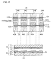
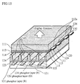
- FIG. 15 shows an example of a conventional AC plane discharge type gas discharge panel.
- This gas discharge panel has a front panel 110 and a back panel arranged opposite each other, sealed around the outer edge with a sealing material composed of low-melting glass to form the gas discharge space.
- the airtight space 104 formed between the two substrates is filled with an inert gas (a mixture of helium and xenon) at a pressure of about 300Torr to 500Torr (40kPa to 66.5kPa).
- the front panel 110 has display electrode pairs 112a, 112b, formed on the opposing face (the side facing the back panel), and has a dielectric layer 113, composed of dielectric glass, and a protective layer 114, composed of MgO, formed as a coating over the electrodes.
- the back panel 120 has address electrodes 122 patterned on the opposing face (the side facing the front panel), and has a back dielectric layer 123 formed as a coating over the electrodes. Barrier ribs 124 are formed on top of the back dielectric layer 123, and RGB phosphor layers 131 are formed between adjacent barrier ribs 124.
- the space 140 delimited by the barrier ribs 124 becomes the light-emitting area (discharge cells), and a phosphor layer is applied to each discharge cell.
- the barrier ribs 124 and address electrodes 122 are formed in the same direction, and the display electrode pairs 112a, 112b, are perpendicular to the address electrodes 122.
- this gas discharge panel after applying an address pulse between the address electrode 122 and the display electrode 112a, based on the image data to be displayed, applies a sustaining pulse to the pair formed by the display electrode 112a and display electrode 112b, thereby selectively causing a sustaining discharge in the discharge cell.
- a sustaining pulse In the discharge cell subject to sustaining discharge, ultraviolet rays are produced, visible light is generated and emitted from the RGB-colored phosphor layers 131, and an image is displayed.
- the barrier ribs 124 divide the discharge space into discharge cells, preventing cross-talk (the phenomenon of discharge mixing across the interface of discharge cells).
- the front glass substrate 111 and back glass substrate 121 are pressed inward by atmospheric pressure.
- the barrier ribs 124 act as a spacer, maintaining the space between the two substrates, with the peaks of the barrier ribs contacting the inner surface of the front panel 110.
- display electrodes 112a, 112b are formed on the front glass substrate 111, a dielectric layer 113 is formed by applying and baking a layer of dielectric glass covering the electrodes, and a protective layer 114 is formed by EB evaporation of MgO over the dielectric layer 113.
- address electrodes 122 are formed on the back glass substrate 121, the back dielectric layer 123 is formed covering the electrodes, and barrier ribs 124 are formed on top of the back dielectric layer 123.
- the barrier ribs 124 may be, for example, formed on the surface of the back dielectric layer 123, then coated with resist. Next, the resist coating may be patterned in stripes, the unnecessary portion of barrier rib material removed by sand blasting, and the coating then baked.
- a phosphor paste is potted by printing or other method and baked to form a phosphor layer 131. This completes production of the back panel 120.
- the front panel 110 and back panel 120 produced as described above, have a low-melting glass applied as a sealing material around their outer edges, are stacked and sealed by baking, then evacuated and the space between the two panels is filled with an inert gas, completing production of the gas discharge panel.
- each discharge cell is affected by the shape of the cell.
- the discharge cells which are arranged in a matrix In order to accurately display color images, it is necessary for the discharge cells which are arranged in a matrix to have a uniform shape. This means that it is necessary for the barrier ribs to have uniform height and width.
- the coating will shrink during baking. This causes difficulty in maintaining a uniform height of the barrier ribs and reduces yield. This in turn increases the production cost of gas discharge panels.
- the gas discharge panel has a first and a second substrate facing each other with a space in between, the space filled with discharge gas to form a discharge space.
- At least one of the first and second substrates has groups of electrode pairs for sustaining discharge arranged on its surface.
- the first substrate has phosphor layers arranged on it, such that a plurality of discharge cells is formed in a matrix pattern along the groups of electrode pairs.
- a gas discharge panel which displays images by selectively illuminating a plurality of discharge cells, incorporates gap members of a certain shape between the first and second substrates, in areas corresponding to the borders between discharge cells, except for the center of the discharge cell.
- a certain shape means the gap members have a particular shape, such as spherical or rod-shaped, and their shape does not change over the process of panel production, i.e., the gap members do not deform during baking as a paste material does.
- the spacing (gap) between the substrates can be precisely prescribed. Also, since the gap members are not placed in the central area of the discharge cells, the gap members do not hinder discharge, and the panel is resistant to discharge failure.
- This type of gas discharge panel can be realized through the following processes: (a) a process for arranging a phosphor layer, which corresponds to the illumination color of the discharge cell, in the desired place on one substrate; (b) a process for affixing gap members of a certain shape on one substrate in a position which corresponds to the border region between discharge cells; and (c) a process for stacking the second substrate on the substrate with the gap members affixed and joining the two substrates.
- the conventional method of applying a phosphor paste is prone to cause mixing of colors between adjacent phosphor layers.
- a method such as pasting a film containing the phosphor element on to the substrate and patterning, it is possible to successfully form phosphor layers on the substrate, which correspond to the illumination color of each discharge cell.
- cross-talk can be prevented if the groups of electrode pairs and their surrounding structures are arranged such that discharge occurs primarily towards the center of each discharge cell, away from the edges of the discharge cells.
- the method of simply arranging gap members on one substrate and joining it with another substrate creates a tendency to have gap members in the center of the discharge cells.
- the gap members in the center of the discharge cells creates a problem of hindering discharge.
- a scheme is necessary to arrange the gap members in the areas of the substrate which correspond to the edges of the discharge cells, and avoid the central areas.
- effective techniques include, for example, forming an adhesive layer in advance in the areas corresponding to edges, or reducing the thickness of the phosphor layer in the areas corresponding to eages.
- the stated objective is achieved also by setting filling pressure of the discharge gas in proximity to atmospheric pressure (within a range of 80% to 120% of atmospheric pressure).
- the stated objective is achieved also in production of gas discharge panels by using (a) a method of mixing gap members in when forming the phosphor layer, and (b) a method of mixing gap members in when forming the dielectric layer.
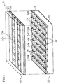
- FIG. 1 is an isometric exploded view of a gas discharge panel according to the first embodiment of the present invention
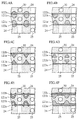
- FIG. 2 is a partial top view and a partial cross-section of the same gas discharge panel.
- Gas discharge panel 1 is formed by a front panel 10 and a back panel 20, joined in parallel across a plurality of gap members 30 (a plurality of glass beads) .
- the two panels 10, 20 are sealed around their outer edges with a sealing material (not shown) composed of low-melting glass, to form a gas discharge space.
- the gas discharge space is filled with an inert gas (e.g., a mixture of helium and xenon) at a pressure of about 300Torr to 500Torr (40kPa to 66.5kPa).
- the front panel 10 has display electrode pairs 12a-12b formed in a stripe pattern on the interior side of the front glass substrate 11.
- a dielectric layer 13 composed of dielectric glass and a protective layer 14 composed of MgO form a coating over the entire surface of the front glass substrate 11, covering the display electrodes 12.
- Each display electrode 12a-12b has a layered structure, formed by a transparent electrode 121a, 121b composed of a thin membrane of ITO or other metallic oxide, covered by a bus electrode 122a, 122b composed a thick film of silver or other metal. As described below, the transparent electrodes 121a, 121b have a particular shape.
- the back panel 20 has address electrodes 22 formed in a stripe pattern on the interior side of the back glass substrate 21.
- a back dielectric layer 23 forms a coating over the address electrodes 22, and phosphor layers 24 of each RGB color are formed in a stripe pattern over the address electrodes 22 on top of the back dielectric layer 23.
- Display electrode pairs 12a-12b are arranged perpendicular to the address electrodes 22, and discharge occurs in the area of the discharge space centered between the intersection of the display electrode pairs 12a-12b and the address electrodes 22.
- the phosphor layer 24 of each color R, G, B faces a discharge cell 40, and three discharge cells 40R, 40G, 40B (shown by broken line in FIG. 2) along a display electrode pair 12a-12b forms one pixel.
- Adjacent phosphor layers 24 are separated by a space where no phosphor is applied (blank area 25).
- Gap members 30 are situated between the front panel 10 and back panel 20, distributed along the blank area 25.
- the gap members 30 are situated between and in contact with the protective layer 14 and the back dielectric layer 23, thereby determining the gap between the front panel 10 and back panel 20.
- the gap members 30 are, in principle, of spherical or other regular form, and composed of a material which has some level of heat-resistance to avoid deformation by heat during the production process of the gas discharge panel.
- Silica material of spherical form is one specific example.
- a driver and driving circuit 100 as shown in FIG. 3 is connected to a gas discharge panel 1 of the above structure, and operated to display image data.
- An address pulse is applied to the address electrode 22 and display electrode 12a, and a sustaining pulse is applied to the display electrode pair 12a-12b, causing a sustaining discharge in the discharge cell chosen in correspondence to the image to be displayed.
- ultraviolet rays are emitted from the discharge cell 40R, 40G, 40B where discharge occurred.
- the phosphor layers 24R, 24G, 24B are excited by the ultraviolet rays and emit visible light, causing display of a color image.
- each discharge cell on each of the pair of a display electrode 12a and display electrode 12b are situated transparent electrodes 121a, 121b, protruding towards each other in island shapes.
- the space between the display electrode 12a and display electrode 12b of each pair is smaller at the center of the discharge cell (the center of the phosphor layer 24) than at the border region (i.e., the blank area 25 formed between phosphor layers 24) between adjacent cells. Therefore, when a pulse is applied to the display electrode pair 12a-12b, discharge occurs primarily in the center of the discharge cell, where the space (discharge gap) is small.
- the transparent electrodes 121a, 121b are shown as rectangular island shapes, but, as shown in FIG. 4 (a) through (e), they could also be egg-shaped (a), semi-circular (b), triangular (c), T-shaped (d) or crescent-shaped (e), and still produce discharge primarily in the center of the discharge cell in similar fashion.
- the transparent electrodes 121a, 121b may also be band-shaped, instead of island-shaped, with protrusions in the center of the discharge cell, and still produce discharge primarily in the center of the discharge cell in similar fashion.
- the transparent electrodes must not necessarily be formed as two separate parts, on display electrodes 12a and 12b. Forming only one transparent electrode 121a as described above on one display electrode 12a, for example, will produce discharge primarily in the center of the discharge cell in similar fashion also.
- Display electrodes 12a and 12b may be formed by all metallic electrodes, and as long as the metallic electrodes have protrusions formed in the center of each discharge cell, will produce discharge primarily in the center of the discharge cell in similar fashion.
- protrusions may be formed in the center of the discharge cell on the bus electrode itself, without using transparent electrodes, and still produce discharge primarily in the center of the discharge cell.
- the gas discharge panel 1 described above has gap members 30 which have a regular form and does not suffer heat-deformation in the production process. This allows the spacing between the front panel 10 and back panel 20 to be precisely regulated. This, in turn, ensures the correct height of the discharge space in each discharge cell. In addition, in production of the gas discharge panel 1, the process of forming barrier ribs can be eliminated, simplifying production.
- the display electrode pair 12a-12b is formed such that, when, as described above, a sustaining pulse is applied, discharge occurs primarily in the center of the discharge cell. This prevents discharge from spreading to the bordering area, and prevents cross-talk.
- the shape of the display electrodes was controlled in order to cause discharge primarily in the center of the discharge cell.
- the display electrode is a simple band-shape, it is also possible to produce discharge primarily in the center of the discharge cell by controlling the surrounding structure, e.g., by controlling the shape of the dielectric layer 13 or the protective layer 14.
- discharge may be focused in the center of the discharge cell by increasing the thickness of the dielectric layer 13 towards the edges of the discharge cell and decreasing the thickness towards the center of the discharge cell (e.g., by layering the dielectric layer while patterning, producing fewer layers in the area facing the phosphor layer 24 and more layers in the area facing the blank area 25).
- This method makes it possible to produce discharge primarily in the center of the discharge cell.
- only the portion of the protective layer 14 towards the center of the discharge cell may be formed of MgO (e.g., by patterning the protective layer, forming a MgO membrane in the area facing the phosphor layer 24 and not forming a MgO membrane in the area facing the blank area 25.).
- This method also produces discharge primarily in the center of the discharge cell, because secondary electrons are more likely to be released during discharge in the area where a MgO protective layer is formed.
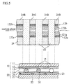
- FIG. 5 shows an abbreviated partial cross-section of the gas discharge panel according to the second embodiment. The following explains the structure of a gas discharge panel with reference to this figure.
- the gas discharge panel of this embodiment is similar to the gas discharge panel shown in FIG. 1.
- the differences, as shown in FIG. 5, are the simple line-shape of the display electrode pairs and the formation of a black matrix 15 on the interior surface of the front glass substrate 11 in the area facing the blank area 25 (the space between adjacent phosphor layers 24).
- cross-talk is more likely to occur than in the first embodiment.
- the black matrix 15 even if cross-talk occurs at the border area of adjacent phosphor layers 24 and causes release of mixed-color light, this light is interrupted by the black matrix 15, so that almost none escapes, controlling loss of picture quality due to color-mixing from cross-talk.
- the mixed light interruption benefit of the black matrix 15 and the discharge cross-talk prevention benefit of the designed display electrode shape make it possible to achieve better image quality.
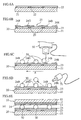
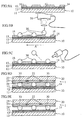
- FIG. 6 (a) to (d) are explanatory diagrams of one example production method for the gas discharge panel described in the first and second embodiments.
- a paste composed of particulate silver, low-melting glass, ethylcellulose resin, and solvent is applied in lines to the surface of the back glass substrate 21 by a printing method.
- the paste then is baked to form address electrodes 22.
- a dielectric paste is applied covering the electrodes and baked to form the back dielectric layer 23.
- FIG. 6 (a) shows the back glass substrate 21 with address electrodes 22 and the back dielectric layer 23 formed on it.
- a green phosphor film containing acrylic photosensitive resin, acrylic resin, and green phosphor powder is applied across the entire surface of the back dielectric layer 23.
- the film is then patterned by exposure in lines to harden the photosensitive resin and developing with a sodium carbonate aqueous solution.
- a red phosphor film and a blue phosphor film are applied and patterned in similar fashion.
- the phosphor layers are baked to form the red, blue, and green phosphor layers 24R, 24B, 24G, as shown in FIG. 6 (b). This completes the back panel 20.
- Patterning is executed such that a blank area 25 is created between adjacent phosphor layers. It is desirable to have no phosphor material present in the blank area 25, but some may be present.
- gap members 30 spherical beads composed of quartz glass are suspended in isopropyl alcohol and controlled.
- a sprayer 50 and the back panel 20 are moved in relation to each other (as arrow A in the figure) and this suspension is sprayed from the sprayer to distribute the gap members 30 over the back panel 20.
- the gap members 30 distributed in this manner become scattered across the blank area 25 on the back panel and on the phosphor layer 24.
- an air gun 51 sprays compressed air on the entire surface of the back panel 20. This removes gap members 30 from the phosphor layer 24, but gap members 30 on the blank area 25 contact the surface of the back dielectric layer 23 and the edge of the phosphor layer 24, and is difficult to remove.
- ratio of the width of the blank area 25 to the width of the gap members 30 is at least 50% and no more than 100%, there is a stronger tendency for the gap members 30 to remain in the blank area 25, so a ratio within this range is desirable.
- the width of the blank area 25 in a range of 50 ⁇ m to 100 ⁇ m.
- the back panel 20 with gap members 30 applied has a front panel situated on top, and the outer edge is sealed with a sealing material and filled with discharge gas to complete the gas discharge panel 1.
- a thin membrane of transparent electrode material is formed by sputtering or other method, and then the transparent electrodes are formed by patterning by etching by photoresist. Then, silver electrode material is printed and baked to form a bus electrode, which comprises the display electrode pair 12a-12b. Then, a dielectric paste is applied to cover the surface of the electrodes and baked to form the dielectric layer 13, and MgO is EB vapor deposited thereon to form the protective layer 14 and complete production of the front panel 10.
- a black matrix 15 is formed on the front panel 10
- a paste containing black pigment an inorganic pigment including transition metals such as iron, chromium, manganese
- low-melting glass low-melting glass
- photosensitive resin may be applied and patterned by photolithography on the surface of the front glass substrate 11.
- the phosphor layers 24R, 24G, 24B are formed by a dry method using photosensitive film, a gas discharge panel produced by this production method will not suffer color mixing, even without barrier ribs to separate adjacent phosphor layers.
- gap members 30 were situated in the center of a discharge cell, that cell would tend to suffer discharge failure and non-lighting. However, in the case of a gas discharge panel produced using the method described above, there are no gap members 30 on the phosphor layers 24R, 24G, 24B, and gap members 30 are distributed across the blank area 25, preventing discharge failure.
- gas discharge panel production method As described here, using the gas discharge panel production method according to this embodiment, production cost can be greatly reduced through elimination of the barrier rib formation process. Furthermore, according to the production method of this embodiment, a gas discharge panel with excellent color display quality can be produced.
- the thick film of acrylic resin or such material will be burned off in the phosphor layer baking process or the sealing material baking process, so as not to remain on the finished gas discharge panel.
- the phosphor layers are formed using a phosphor film which includes photosensitive resin, patterned by photolithography.
- a phosphor film which includes photosensitive resin, patterned by photolithography.
- the phosphor layers 24 were baked first, followed by distribution of the gap member glass beads.
- the gap members may be distributed without baking, and the front panel 10 joined to the back panel 20, and the gap members may be baked together in the same process with the sealing material.
- low-melting glass may be applied to the surface of the gap member 30 glass beads before baking.
- the sealing material when the sealing material is baked in the sealing process, the low-melting glass on the surface of the glass beads will melt, thereby joining the gap members 30 to the front panel 10 and the back panel 20. Therefore, by this method, a gas discharge panel can be produced whose front panel 10 and back panel 20 are joined via the gap members 30. In this case, the gap between the two panels 10, 20 can be accurately maintained even with discharge gas filled to higher than atmospheric pressure.
- gap members 30 can be removed from the phosphor layers 24 by agitation of the back panel 20 as well.
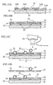
- FIGS. 7 (a) through 7 (e) describe an example of the production method of a gas discharge panel as described in Embodiments 1 and 2.
- address electrodes 22, which correspond to the back dielectric layer 23, are formed on the back glass substrate, and the back dielectric layer 23 was formed thereon, followed by formation of an adhesive layer 26 on top of the back dielectric layer 23.
- FIG. 7 (a) shows the back dielectric layer 23 with the adhesive layer 26 formed on top.
- the adhesive layer 26 is formed of a material which has adhesion, e.g., an adhesive resin such as an epoxy resin. Using a reverse coater, a solution of the epoxy resin and isopropanol is applied and dried to form the adhesive layer 26.
- an adhesive resin such as an epoxy resin.
- the phosphor layers 24R, 24G, 24B are formed (FIG. 7 (b)), gap members 30 are distributed over the entire surface (FIG. 7 (c)), compressed air (or vibration) is used to remove gap members from the phosphor layers 24 (FIG. 7 (d)).
- the adhesive layer 26 is exposed in the blank area 25, so that the gap members 30 applied to the blank area 25 are strongly attached as compared to the case of Example 1.
- the front panel 10 is stacked on the back panel 20, which has gap members 30 applied to it, the outer edges are sealed with sealing material, and discharge gas is inserted to complete the gas discharge panel 1.
- an adhesive layer 26 can be created by the process described above, without negatively affecting discharge in the finished gas discharge panel.
- FIGS. 8 (a) through (e) describe an example of a production method for the gas discharge panel described in Embodiments 1 and 2.
- first address electrodes 22 are formed on the back glass substrate 21, and a dielectric paste is applied over the electrodes to form an unbaked back dielectric layer 23a (FIG.8 (a)). Then, without baking this, phosphor layers 24R, 24G, 24B formed on top (FIG.8(b)).
- gap members 30 are distributed over the entire surface (FIG.8(c)), and gap members 30 on the phosphor layers 24 are removed by compressed air (or agitation) (FIG.8(d)).
- gap members 30 in the blank area 25 are pressed into the unbaked back dielectric layer 23a, causing the gap members 30 to be partially buried and fixed.
- the front panel 10 is stacked on the back panel 20, which has gap members 3C applied to it.
- the two panels 10, 20 are compressed such that the gap between them is uniform, sealed around their outer edges with sealing material and filled with discharge gas.
- the unbaked back dielectric layer 23a can be baked simultaneously with the sealing material. This baking forms the back dielectric layer 23 to complete the gas discharge panel.
- the gap members 30 and the back dielectric layer 23 are joined with part of the gap members 30 buried in the dielectric layer 23.
- first the phosphor layers 24 are baked, followed by distribution of the glass bead gap members 30.
- FIG. 9 shows an example of a production method for the gas discharge panel described in Embodiments 1 and 2.
- a thick film 16 is formed in a stripe pattern over the protective layer 14 on the front panel 10.
- a blank area 17 is formed between adjacent thick films.
- this thick film 16 has properties such that it will be burned off when heat or other energy is applied, with acrylic or other resins used here.
- the thick film 16 is formed in areas which will be opposite the phosphor layers 24 when the gas discharge panel is finished (i.e., areas corresponding to the center of the discharge cells).
- a method of printing a resin paste may be used, or a method of applying a photosensitive resin paste or a photosensitive resin film and patterning by photolithography.
- gap members 30 are distributed across the entire surface of the front panel 10 (FIG. 9 (b)), and removed from the thick film 16 by compressed air (or vibration) (FIG.9(c)).
- gap members 30 are disposed in a distribution across the blank area 17 between adjacent thick films 16.
- the back panel 20 is produced as described in FIG. 6 (a), (b) for Example 1.
- the back panel 20 is joined to the front panel 10, which has gap members 30 disposed on it.
- the gap members 30 are caught in the blank area 25 between adjacent phosphor layers 24.
- the two panels 10, 20 are sealed around their edges with sealing material.
- the thick film 16 is baked simultaneously with the sealing material and burned off, so that no thick film 16 remains after sealing, as shown in FIG. 9(e). Then, discharge gas is filled to complete the gas discharge panel 1.
- a gas discharge panel 1 can also be produced by a method of forming the thick film 16, which regulates the locations where gap members 30 are disposed, on the front panel 10, and dispersing gap members 30 over the top.
- FIGS. 10 (a) to (d) show an example of a production method for the gas discharge panel described in Embodiments 1 and 2.
- a back panel 20 is prepared, by forming address electrodes 22 on the back glass substrate 21 and forming a back dielectric layer 23 and phosphor layers 24 on top, as in FIGS. 6(a) and (b) of Example 1 above.
- a mask plate 52 with cut-out portions corresponding to the locations of blank areas 25 is placed over the back panel, so that only portions corresponding to phosphor layers 24 are covered.
- the extent covered by the mask plate 52 is adjusted according to the size of the gap members 30 (diameter of the glass beads) , but the center regions of the phosphor layers 24 must be covered.
- gap members 30 are dispersed across the entire surface of the front panel 10 (FIG. 10 (c)).
- the surface of the glass beads, which are the gap members 30 to be dispersed is coated with an adhesive material (e.g., epoxy resin) to form an adhesive layer 31 beforehand.
- an adhesive material e.g., epoxy resin
- the gap members 30 located in the blank area 25 remain on the back panel 20, and the gap members 30 disposed on the mask plate 52 are removed from the back panel 20.
- an adhesive layer 31 fuses the gap members 30 securely to the blank area 25, and prevents gap members 30 in the blank area 25 from becoming dislodged when the mask plate 52 is removed.
- the front panel 10 is joined to the back panel 20, which has gap members 30 disposed on it, and discharge gas is filled to complete the gas discharge panel 1.
- the adhesive layer 31 is burned off when it is baked with the sealing material during the sealing process, so that it does not remain in the finished gas discharge panel.
- the mask plate 52 may be laid over the front panel 10 and gap members 30 are dispersed over it, then, when the mask plate is removed, gap members 30 will be left in areas of the front panel 10 which correspond to the blank areas. Joining the back panel 20 thereto produces a similar gas discharge panel.
- spherical glass beads are used for the gap members 30, but the gap members 30 are not limited to spherical forms, as any shape which can regulate the gap between the two panels 10, 20 when disposed in the blank areas is acceptable.
- rod-shaped gap members 30 composed of fibers such as glass fibers (the fibers may also be hollow tubes), disposed in the blank areas 25.
- This sort of rod-like gap members 30, disposed in the blank areas 25, also perform the function of barrier ribs, controlling cross-talk.
- rod-like gap members 30 may also be placed at intervals (e.g., in every other blank space).
- an angular rod as shown in FIG. 12 may also be used.
- the gap member 30 shown in FIG. 12 has a phosphor layer 32 formed on its surface, in the same color as the phosphor layer facing it.
- the side of a gap member 30 facing a red phosphor layer 24R is covered with a red phosphor layer 32R
- the side of a gap member 30 facing a green phosphor layer 24G is covered with a green phosphor layer 32G
- the side of a gap member 30 facing a blue phosphor layer 24B is covered with a blue phosphor layer 32B.
- each discharge cell By also forming phosphor layers 32 on the gap members 30, the discharge space of each discharge cell has phosphor layers 24 and phosphor layers 32 facing it, increasing the illumination efficiency of each discharge cell.
- FIG. 13 shows an abbreviated partial cross-section of a gas discharge panel according to this embodiment. The following is an explanation of the structure of such a gas discharge panel with reference to this figure.
- a gas discharge panel of this embodiment has discharge gas filled to near atmospheric pressure (in the vicinity of 760Torr to 1013Torr), and in principle does not use gap members, but is otherwise similar in configuration to the gas discharge panel described by FIG. 1 above.
- conventional gas discharge panels contain discharge gas at much lower than atmospheric pressure, meaning that without a dense structure of barrier ribs or gap members in the display area, the space between the front and back panels cannot be properly maintained.
- this embodiment sets discharge gas pressure in proximity to atmospheric pressure, maintaining a balance between internal and external gas pressure. Therefore, the space between the front and back panels can be properly maintained without a dense structure of barrier ribs or gap members in the display area, or without any barrier ribs or gap members in the display area at all.
- the filling pressure in a range of 80% to 120% of atmospheric pressure, matched to the atmospheric pressure of the location of use.
- the type of gas discharge panel here eliminates the process of placing gap members o the substrate, and has filling pressure of the discharge gas set at near atmospheric pressure, but otherwise can be produced in the same manner as Example 1 above. However, it is necessary to maintain the space between the two substrates during the sealing process, using a method such as placing gap members around the periphery of the substrates.
- this type of gas discharge panel may be produced using beads of a material such as plastic which is destroyed by heat.
- this type of gas discharge panel may be produced using the production method of Example 1 above, by substituting beads of a material decomposed by heat for the glass beads and setting discharge gas filling pressure to near atmospheric pressure.
- barrier ribs As described here, according to this embodiment, it is not necessary to form barrier ribs, nor are gap members necessary in principle, so that it is possible to produce a gas discharge panel even more simply than by the methods of Embodiments 1 and 2.
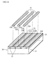
- FIG. 14 shows an exploded isometric view of a gas discharge panel according to this embodiment.
- This gas discharge panel is similar to the gas discharge panel 1 described in Embodiment 1, but instead of locating gap members 30 in the blank areas 25, gap members 30 are distributed across the phosphor layers 24R, 24G, 24B.
- This type of gas discharge panel may be produced by the following method.
- address electrodes 22 are formed on the back glass substrate 21, and a back dielectric layer 23 is formed covering them.
- phosphor layers are formed using a photosensitive phosphor film in each color, but gap members 30, glass beads, are fixed in the film in advance.
- green phosphor film is applied across the entire surface of the back dielectric layer 23, and the film is patterned in a line form by exposure to light.
- red film and blue film are applied and patterned in similar fashion.
- this assembly is baked to form red, green and blue phosphor layers 24R, 24G, 24B.
- the back panel 20 shown in FIG. 14 is produced.
- a front panel 10 is situated on top of the back panel, which has gap members 30 placed on it, the edges of the panels are sealed with sealing material and discharge gas is filled, completing the gas discharge panel.
- the gas discharge panel of this embodiment has gap members 30 on the phosphor layers 24R, 24G, 24B, and in the center area of the discharge cells, creating a greater tendency towards discharge failure than in Embodiments 1 through 4 above, but the space between the front and back panels 10, 20 can be precisely maintained. Also, since gap members 30 are placed in the process of forming the phosphor layers, it is not necessary to form gap members in a separate step as in Embodiments 1 through 3, creating an advantage in ease of production.
- gap members 30 may be included in the dielectric layer 13.
- Embodiments 1 through 5 above used a surface discharge type gas discharge panel as an example for explanatory purposes, but for an opposed discharge type gas discharge panel also, by arranging the front and back panels such that sustaining electrode pairs intersect each other, a gas discharge panel with gap members that displays color images can be created in similar fashion to the plane-discharge type gas discharge panel described above.
- an opposed discharge type gas discharge panel has front and back panels situated such that sustaining electrode pairs intersect each other, so that sustaining discharge occurs centered at the intersections.
- sustaining electrode pairs intersect each other, so that sustaining discharge occurs centered at the intersections.
- discharge can be more reliably concentrated in the center areas of the discharge cells.
- the gas discharge panel and method of gas discharge panel production of the present invention are suited for use in color display devices, especially large-format color display devices, such as those used in computers and televisions.
Landscapes
- Engineering & Computer Science (AREA)
- Physics & Mathematics (AREA)
- Plasma & Fusion (AREA)
- Manufacturing & Machinery (AREA)
- Gas-Filled Discharge Tubes (AREA)
Abstract
Description
Claims (33)
- A gas discharge panel, which comprises (a) a first substrate and a second substrate facing each other across an interval, the interval forming a discharge space and being filled with discharge gas, (b) pairs of electrodes for sustaining discharge provided on at least one of the substrates, (c) a plurality of discharge cells formed in a pattern along the electrode pairs, and (d) a plurality of phosphor layers formed by baking a phosphor film and provided on the first substrate facing the discharge cells, each phosphor layer corresponding to an illumination color of the discharge cell, and the gas discharge panel displaying a color image by selectively illuminating the discharge cells, wherein
a plurality of gap members of a given shape are disposed at locations corresponding to boundary areas between and excluding the center areas of the discharge cells, so as to separate the first substrate and second substrate, and determine the interval between the first substrate and second substrate. - The gas discharge panel of Claim 1, wherein
the electrode pairs and their surrounding structures are provided such that, when a voltage is applied to the electrode pairs and sustaining discharge is caused, discharge primarily occurs in the center of the discharge cells, rather than near the boundaries. - The gas discharge panel of Claim 2, whereinthe electrode pairs comprise a plurality of linear electrodes, provided in a stripe pattern on the second substrate, andan interval between the linear electrodes forming the pairs is smaller in the center of the discharge cells than toward the boundaries of the discharge cells.
- The gas discharge panel of Claim 2, whereineach electrode pair has a transparent electrode, andthe transparent electrode has a shape such that an interval between the linear electrodes forming the pair is smaller in the center of the discharge cell than toward the boundaries of the discharge cell.
- The gas discharge panel of Claim 2, whereineach electrode pair is covered with a dielectric layer in an area toward the discharge space, andthe dielectric layer has a thickness which is smaller in the center of the discharge cell than toward the boundaries of the discharge cell.
- The gas discharge panel of Claim 2, whereineach electrode pair is covered with a dielectric layer in an area toward the discharge space, andthe dielectric layer is covered with a layer of magnesium oxide in an area toward the center of the discharge cell and excluding the boundary area.
- The gas discharge panel of any of Claims 1 through 5, wherein
the second substrate has a black matrix formed in areas corresponding to boundary areas. - The gas discharge panel of any of Claims 1 through 4, wherein
the phosphor layers are thinner towards the boundaries than in the center areas. - The gas discharge panel of Claim 8, whereina dielectric layer is provided on the first substrate,the phosphor layers are provided on the dielectric layer, andthe gap members are partially buried in the dielectric layer.
- The gas discharge panel of Claim 8, whereinthe electrode pairs comprise a plurality of linear electrodes, provided in a stripe pattern on the second substrate, andthe phosphor layers are provided in a stripe pattern in a direction which intersects with the electrode pairs.
- The gas discharge panel of Claim 1, whereina dielectric layer is provided on the second substrate, andthe gap members are partially buried in the dielectric layer.
- The gas discharge panel of Claim 1, wherein
a phosphor element is applied to their surfaces of the gap members. - The gas discharge panel of Claim 1, wherein
the gap members have a spherical or rod-like shape. - The gas discharge panel of Claim 1, wherein
the gap members are in contact with at least one of the first substrate and second substrate. - A gas discharge panel having a first substrate and a second substrate, facing each other across an interval, the interval forming a discharge space and filled with discharge gas, pairs of electrodes for sustaining discharge provided on at least one of the substrates, a plurality of discharge cells formed in a matrix pattern along the electrode pairs, a plurality of phosphor layers, formed by baking a phosphor film and corresponding to an illumination color of each discharge cell, provided on the first substrate facing the discharge cells, and which displays a color image by selectively illuminating the discharge cells, whereinthe discharge gas is filled to a pressure of from 80 percent to 120 percent, inclusive, of atmospheric pressure,the first substrate and second substrate contact each other around the outside of a image display area, andthe first substrate and second substrate do not contact each other across a plurality of discharge cells in two dimensions of the image display area.
- The gas discharge panel of Claim 15, wherein
the electrode pairs and their surrounding structures are provided such that, when a voltage is applied to the electrode pairs and sustaining discharge is caused, discharge primarily occurs in the center of the discharge cells, rather than near the boundaries. - (cancelled)
- A gas discharge panel display device, which displays an image by selectively illuminating the plurality of discharge cells, comprising:the gas discharge panel of Claim 1 or Claim 15, anda driving unit, which applies a voltage to the electrode pairs for sustaining discharge.
- A method for production of a gas discharge panel, the panel having discharge cells of each color arranged in a matrix pattern formed between a first substrate and a second substrate, the production method comprising:a phosphor layer forming process, for providing a phosphor layer corresponding to an illumination color of each discharge cell on the first substrate,a gap member distribution process, for disposing gap members of a given shape at locations on the first substrate and the second substrate corresponding to boundaries between discharge cells, anda stacking process, for joining the first substrate and the second substrate after gap members have been applied to one of the substrates.
- The gas discharge panel production method of Claim 19, whereinthe phosphor layer forming process is conducted before the gap member distribution process, andthe phosphor layers on the first substrate are formed so as to be thicker towards the center of the discharge cells than in areas corresponding to the boundaries.
- The gas discharge panel production method of Claim 20, wherein
an area where phosphor layers are not formed in the phosphor layer forming process has a width of at least 50 percent and not more than 100 percent of the interval between the substrates as determined by the gap members. - The gas discharge panel production method of Claim 20, in which the gap members have a shape so as to fit into the boundary areas between the phosphor layers of adjacent discharge cells, wherein
the gap member distribution process includes:a distribution step, for spreading gap members over the first substrate, anda removal step, for removing the gap members distributed on the phosphor layers. - The gas discharge panel production method of Claim 20, wherein
the phosphor layer formation process includes a phosphor film application step, for applying a film containing phosphor element of each color to locations corresponding to the discharge cells on the first substrate. - The gas discharge panel production method of Claim 23, wherein
in the phosphor film application step, the phosphor element film including photosensitive material is applied to the first substrate and patterned by exposure to light. - The gas discharge panel production method of Claim 23, wherein
in the phosphor layer formation process, the phosphor element film is applied to areas of the first substrate excluding areas corresponding to boundaries. - The gas discharge panel production method of Claim 20, whereina dielectric layer application process, for applying a dielectric element paste to the surface of the first substrate, is provided before the phosphor layer forming process, andthe applied dielectric element paste is baked after the gap member distribution process.
- The gas discharge panel production method of Claim 19, wherein
the gap member distribution process includes:an adhesive layer forming step, for providing an adhesive layer in areas of the first substrate or the second substrate corresponding to the boundaries, anda gap member distribution step, for spreading gap members over the adhesive layer. - The gas discharge panel production method of Claim 27, wherein
the gap member distribution process includes, after the gap member distribution step, a removal step, for removing the gap members located in areas of the first substrate or the second substrate other than on the adhesive layer. - The gas discharge panel production method of Claim 22 or Claim 27, wherein
in the removal step, gap members are removed by blowing gas over or by agitating the substrate to which gap members were applied. - The gas discharge panel production method of Claim 19, wherein
the gap member distribution process includes:a mask locating step, for applying a mask, which covers an area corresponding to the center of each discharge cell where gap members are to be distributed, and which has an opening at the boundaries,a spreading step, for spreading gap members over the mask, anda detaching step, for removing the mask from the substrate. - The gas discharge panel production method of Claim 30, further comprising:
an adhesive application process, before the gap member distribution process, for applying an adhesive material to surfaces of the gap members. - A method for production of a gas discharge panel, comprising:an electrode forming process, for forming electrodes on a first substrate,a dielectric element material application process, for applying a dielectric element material to cover the electrodes,a dielectric element baking process, for baking the applied dielectric element, andafter the dielectric element material application process, a stacking process, for joining the first substrate to a second substrate.
- A method for production of a gas discharge panel, comprising:a phosphor element material application process, for applying a phosphor element material, which contains gap members, to a first substrate,a phosphor element baking process, for baking the applied phosphor element material to form a phosphor layer, and,after the phosphor element material application process, a stacking process, for joining the first substrate to a second substrate.
Applications Claiming Priority (3)
| Application Number | Priority Date | Filing Date | Title |
|---|---|---|---|
| JP29632699 | 1999-10-19 | ||
| JP29632699 | 1999-10-19 | ||
| PCT/JP2000/007224 WO2001029863A1 (en) | 1999-10-19 | 2000-10-18 | Gas discharge panel and method for manufacturing gas discharge panel |
Publications (2)
| Publication Number | Publication Date |
|---|---|
| EP1150322A1 true EP1150322A1 (en) | 2001-10-31 |
| EP1150322A4 EP1150322A4 (en) | 2008-05-28 |
Family
ID=17832098
Family Applications (1)
| Application Number | Title | Priority Date | Filing Date |
|---|---|---|---|
| EP00969845A Withdrawn EP1150322A4 (en) | 1999-10-19 | 2000-10-18 | PLASMA PANEL AND METHOD FOR MANUFACTURING THE SAME |
Country Status (6)
| Country | Link |
|---|---|
| US (2) | US6692325B1 (en) |
| EP (1) | EP1150322A4 (en) |
| KR (1) | KR100767929B1 (en) |
| CN (1) | CN1264184C (en) |
| TW (1) | TW478007B (en) |
| WO (1) | WO2001029863A1 (en) |
Cited By (2)
| Publication number | Priority date | Publication date | Assignee | Title |
|---|---|---|---|---|
| WO2004107379A1 (en) * | 2003-05-28 | 2004-12-09 | Tokyo Ohka Kogyo Co., Ltd. | Unbaked laminate for producing front plate of plasma display device, and method for producing front plate of plasma display device |
| WO2003009329A3 (en) * | 2001-07-17 | 2004-12-16 | Inst Niedertemperatur Plasmaph | Device for producing gas discharges, constructed according to the dialectrically impeded discharge principle, for light sources and visual display devices |
Families Citing this family (8)
| Publication number | Priority date | Publication date | Assignee | Title |
|---|---|---|---|---|
| KR100822185B1 (en) * | 2001-10-10 | 2008-04-16 | 삼성에스디아이 주식회사 | Touch panel |
| JP3942166B2 (en) | 2002-07-23 | 2007-07-11 | 株式会社日立プラズマパテントライセンシング | Method for manufacturing substrate structure of gas discharge panel |
| TWI225561B (en) * | 2002-12-18 | 2004-12-21 | Au Optronics Corp | A liquid crystal display |
| US20050206297A1 (en) * | 2004-03-18 | 2005-09-22 | Multimedia Electronics, Inc. | Luminous display device with increased active display and method of making the same |
| EP1640946A3 (en) * | 2004-09-24 | 2008-05-14 | Pioneer Corporation | Plasma display apparatus |
| KR100648728B1 (en) * | 2004-11-30 | 2006-11-23 | 삼성에스디아이 주식회사 | Plasma display panel |
| KR20060091669A (en) * | 2005-02-16 | 2006-08-21 | 엘지전자 주식회사 | Black Matrix Composition for Plasma Display Panel Front Panel |
| US20080012494A1 (en) * | 2006-07-14 | 2008-01-17 | Chunghwa Picture Tubes, Ltd | Plasma display panel |
Family Cites Families (30)
| Publication number | Priority date | Publication date | Assignee | Title |
|---|---|---|---|---|
| US4024613A (en) * | 1975-01-02 | 1977-05-24 | Owens-Illinois, Inc. | Method of permanently attaching metallic spacers in gaseous discharge display panels |
| JPS5273672A (en) * | 1975-12-16 | 1977-06-20 | Fujitsu Ltd | Gas discharge panel |
| JPS60107233A (en) * | 1983-11-14 | 1985-06-12 | Fujitsu Ltd | Method of manufacturing panel for gas discharge |
| JPS6315528A (en) | 1986-07-08 | 1988-01-22 | Nec Corp | Semiconductor device |
| JPS63155528A (en) * | 1986-12-18 | 1988-06-28 | Fujitsu Ltd | Manufacture of surface discharge type gas discharge panel |
| JPS6465743A (en) | 1987-09-04 | 1989-03-13 | Fujitsu Ltd | Manufacture of plasma display panel |
| JPH01175146A (en) * | 1987-12-28 | 1989-07-11 | Fujitsu Ltd | Manufacture of gas discharge panel |
| JPH01183029A (en) * | 1988-01-07 | 1989-07-20 | Fujitsu Ltd | Manufacture of gas discharge panel |
| JP3123053B2 (en) * | 1990-02-06 | 2001-01-09 | 日本電気株式会社 | Gas discharge display element and driving method thereof |
| JPH0479126A (en) * | 1990-07-20 | 1992-03-12 | Fujitsu Ltd | Plasma display panel |
| JPH0495331A (en) * | 1990-07-31 | 1992-03-27 | Mitsubishi Electric Corp | Plasma display panel |
| JP2596279B2 (en) | 1992-01-30 | 1997-04-02 | 双葉電子工業株式会社 | Enclosure support pillar formation method |
| JP3187589B2 (en) | 1993-02-08 | 2001-07-11 | 三菱電機株式会社 | Flat type light source and method of manufacturing the same |
| JPH0895239A (en) * | 1994-09-20 | 1996-04-12 | Nippon Synthetic Chem Ind Co Ltd:The | Photoresist film |
| US5658832A (en) * | 1994-10-17 | 1997-08-19 | Regents Of The University Of California | Method of forming a spacer for field emission flat panel displays |
| JPH08250030A (en) | 1995-03-14 | 1996-09-27 | Pioneer Electron Corp | Plasma display panel |
| JP3224486B2 (en) | 1995-03-15 | 2001-10-29 | パイオニア株式会社 | Surface discharge type plasma display panel |
| JP3212837B2 (en) * | 1995-06-30 | 2001-09-25 | 富士通株式会社 | Plasma display panel and method of manufacturing the same |
| JP3233829B2 (en) | 1995-09-13 | 2001-12-04 | 新日本製鐵株式会社 | High-strength PC steel rod excellent in delayed fracture characteristics of spot welds and method of manufacturing the same |
| JPH0992162A (en) * | 1995-09-20 | 1997-04-04 | Hitachi Ltd | Plasma display panel |
| JP3339554B2 (en) * | 1995-12-15 | 2002-10-28 | 松下電器産業株式会社 | Plasma display panel and method of manufacturing the same |
| JPH09213215A (en) * | 1996-01-30 | 1997-08-15 | Nippon Sheet Glass Co Ltd | Manufacture of plasma display device and glass board for plasma display device |
| US5747931A (en) * | 1996-05-24 | 1998-05-05 | David Sarnoff Research Center, Inc. | Plasma display and method of making same |
| JP3209925B2 (en) * | 1996-07-11 | 2001-09-17 | 富士通株式会社 | Plasma display panel and partition wall forming method |
| EP1229568B1 (en) | 1996-09-18 | 2003-12-10 | Matsushita Electric Industrial Co., Ltd | Production method of plasma display panel suitable for minute cell structure, the plasma display panel, and for displaying the plasma display panel |
| JPH10149773A (en) * | 1996-11-18 | 1998-06-02 | Dainippon Printing Co Ltd | Plasma display panel |
| JPH10302645A (en) | 1997-04-22 | 1998-11-13 | Matsushita Electric Ind Co Ltd | Gas discharge panel |
| JP3774046B2 (en) * | 1997-10-15 | 2006-05-10 | 大日本印刷株式会社 | Phosphor composition, phosphor paste and photosensitive dry film |
| KR19990062412A (en) * | 1997-12-05 | 1999-07-26 | 손욱 | Helium discharge display |
| US6252353B1 (en) * | 1997-12-17 | 2001-06-26 | Lg Electronics Inc. | Color plasma display panel |
-
2000
- 2000-10-18 TW TW089121808A patent/TW478007B/en not_active IP Right Cessation
- 2000-10-18 EP EP00969845A patent/EP1150322A4/en not_active Withdrawn
- 2000-10-18 KR KR1020017007743A patent/KR100767929B1/en not_active Expired - Fee Related
- 2000-10-18 CN CNB008038899A patent/CN1264184C/en not_active Expired - Fee Related
- 2000-10-18 US US09/868,354 patent/US6692325B1/en not_active Expired - Fee Related
- 2000-10-18 WO PCT/JP2000/007224 patent/WO2001029863A1/en not_active Ceased
-
2003
- 2003-07-16 US US10/621,023 patent/US7023136B2/en not_active Expired - Fee Related
Cited By (4)
| Publication number | Priority date | Publication date | Assignee | Title |
|---|---|---|---|---|
| WO2003009329A3 (en) * | 2001-07-17 | 2004-12-16 | Inst Niedertemperatur Plasmaph | Device for producing gas discharges, constructed according to the dialectrically impeded discharge principle, for light sources and visual display devices |
| WO2004107379A1 (en) * | 2003-05-28 | 2004-12-09 | Tokyo Ohka Kogyo Co., Ltd. | Unbaked laminate for producing front plate of plasma display device, and method for producing front plate of plasma display device |
| KR100709526B1 (en) * | 2003-05-28 | 2007-04-20 | 도오꾜오까고오교 가부시끼가이샤 | Unbaked laminate for producing front plate of plasma display device, and method for producing front plate of plasma display device |
| US7563146B2 (en) | 2003-05-28 | 2009-07-21 | Tokyo Ohka Kogyo Co., Ltd. | Unbaked laminate for producing front plate of plasma display device, and method for producing front plate of plasma display device |
Also Published As
| Publication number | Publication date |
|---|---|
| WO2001029863A1 (en) | 2001-04-26 |
| US7023136B2 (en) | 2006-04-04 |
| KR100767929B1 (en) | 2007-10-17 |
| CN1340207A (en) | 2002-03-13 |
| CN1264184C (en) | 2006-07-12 |
| US20040085021A1 (en) | 2004-05-06 |
| KR20010082377A (en) | 2001-08-29 |
| US6692325B1 (en) | 2004-02-17 |
| TW478007B (en) | 2002-03-01 |
| EP1150322A4 (en) | 2008-05-28 |
Similar Documents
| Publication | Publication Date | Title |
|---|---|---|
| US5763139A (en) | Plasma display panel and method for manufacturing the same | |
| EP2226829A1 (en) | A surface discharge plasma display panel and a manufacturing method therefor | |
| US6692325B1 (en) | Gas discharge panel and method for manufacturing gas discharge panel | |
| US6942535B2 (en) | Plasma display panel and the manufacturing method thereof | |
| JP3975168B2 (en) | Flat discharge display | |
| JP3888411B2 (en) | Plasma display panel and manufacturing method thereof | |
| JP3757334B2 (en) | Manufacturing method of surface discharge type plasma display panel | |
| JP3366297B2 (en) | Surface discharge type plasma display panel | |
| US6737806B2 (en) | Plasma display panel including transparent electrode layer | |
| JP2629809B2 (en) | Method of manufacturing gas discharge panel | |
| JP3757333B2 (en) | Manufacturing method of surface discharge type plasma display panel | |
| JP3394219B2 (en) | Method of manufacturing surface discharge type plasma display panel | |
| JPH01276531A (en) | Gas discharge type panel and its manufacturing method | |
| KR100925093B1 (en) | Plasma display panel manufacturing method | |
| JP2001189137A (en) | Gas discharge panel and method of manufacturing gas discharge panel | |
| EP1045421A1 (en) | Flat display device and fabricating method of the same | |
| KR100718055B1 (en) | Method for manufacturing fluorescent layer of plasma display panel | |
| JP4857562B2 (en) | Flat display panel | |
| JP3366296B2 (en) | Surface discharge type plasma display panel | |
| US20070085479A1 (en) | Plasma display panel (PDP) and its method of manufacture | |
| JP4865628B2 (en) | Back plate for plasma display panel and manufacturing method thereof | |
| JP2000299061A (en) | Flat display device and method of manufacturing the same | |
| JP2010062001A (en) | Plasma display panel, and method of manufacturing the same | |
| JP2008123938A (en) | Plasma display panel | |
| JP2008123834A (en) | Plasma display panel |
Legal Events
| Date | Code | Title | Description |
|---|---|---|---|
| PUAI | Public reference made under article 153(3) epc to a published international application that has entered the european phase |
Free format text: ORIGINAL CODE: 0009012 |
|
| 17P | Request for examination filed |
Effective date: 20010709 |
|
| AK | Designated contracting states |
Kind code of ref document: A1 Designated state(s): AT BE CH CY DE DK ES FI FR GB GR IE IT LI LU MC NL PT SE |
|
| AX | Request for extension of the european patent |
Free format text: AL;LT;LV;MK;RO;SI |
|
| RBV | Designated contracting states (corrected) |
Designated state(s): DE FR GB IT |
|
| A4 | Supplementary search report drawn up and despatched |
Effective date: 20080428 |
|
| 17Q | First examination report despatched |
Effective date: 20080725 |
|
| RAP1 | Party data changed (applicant data changed or rights of an application transferred) |
Owner name: PANASONIC CORPORATION |
|
| GRAP | Despatch of communication of intention to grant a patent |
Free format text: ORIGINAL CODE: EPIDOSNIGR1 |
|
| STAA | Information on the status of an ep patent application or granted ep patent |
Free format text: STATUS: THE APPLICATION IS DEEMED TO BE WITHDRAWN |
|
| 18D | Application deemed to be withdrawn |
Effective date: 20110726 |