EP1150221A2 - Apparat zur Simulation von Halbleiterbauelementen, Verfahren und Speichermedium mit entsprechendem Simulationsprogramm - Google Patents
Apparat zur Simulation von Halbleiterbauelementen, Verfahren und Speichermedium mit entsprechendem Simulationsprogramm Download PDFInfo
- Publication number
- EP1150221A2 EP1150221A2 EP01109783A EP01109783A EP1150221A2 EP 1150221 A2 EP1150221 A2 EP 1150221A2 EP 01109783 A EP01109783 A EP 01109783A EP 01109783 A EP01109783 A EP 01109783A EP 1150221 A2 EP1150221 A2 EP 1150221A2
- Authority
- EP
- European Patent Office
- Prior art keywords
- potential
- semiconductor device
- initial value
- physical quantity
- external circuit
- Prior art date
- Legal status (The legal status is an assumption and is not a legal conclusion. Google has not performed a legal analysis and makes no representation as to the accuracy of the status listed.)
- Withdrawn
Links
Images


Classifications
-
- G—PHYSICS
- G06—COMPUTING OR CALCULATING; COUNTING
- G06F—ELECTRIC DIGITAL DATA PROCESSING
- G06F30/00—Computer-aided design [CAD]
- G06F30/20—Design optimisation, verification or simulation
- G06F30/23—Design optimisation, verification or simulation using finite element methods [FEM] or finite difference methods [FDM]
-
- G—PHYSICS
- G06—COMPUTING OR CALCULATING; COUNTING
- G06F—ELECTRIC DIGITAL DATA PROCESSING
- G06F2111/00—Details relating to CAD techniques
- G06F2111/10—Numerical modelling
Definitions
- the present invention relates to a semiconductor device simulation technology to experimentally create operation of a semiconductor device by numerical analysis.
- a semiconductor device will be referred to simply as “device” as follows.
- Device numerical analysis uses “drift-diffusion model” approximating carriers (electrons and holes) as a fluid and “energy-transportation model” approximating them at a higher level widely
- the biases are renewed sequentially so that these five equations of the charge conservation equation, the electron current continuity equation, the hole current continuity equation, the electron energy conservation equation and the hole energy conservation equation are calculated. Since these are non-linear equations, solutions are given by iterative calculation generally called "Newton method.”
- the Newton method is a technique as follows.
- F(x 0 + ⁇ x 0 ) undergoes Taylor expansion on ⁇ x 0 to be expressed as follows.
- x 1 x 0 + ⁇ x 0
- FIG. 16 is a model view having illustrated this procedure.
- the intersection between a tangent and the x axis as the next x value comes closer to a solution. Closer the given initial value comes to the solution, fewer times of required repetitions will do to give a solution, and thus the calculation time up to obtainment of the solution is short.
- the technique described above is a Newton method.
- the number of variant of equations was one in description of the above described Newton method. However, in the device simulation, a mesh is created across the analyzed region and equations are set on variants falling in the meshed points.
- An example of the analysis mesh is shown in FIG. 20. That is, since coulomb potential, the density of electron, the hole density, the electron temperature and the hole temperature appear as variants in a number of the mesh points N, simultaneous equations in 5N units will be solved.
- the above described electric charge conservation equation, electron current continuity equation, hole current continuity equation, electron energy conservation equation and hole energy conservation equation are expressed in the form in which the right side components thereof were transposed by the following equation.
- F ⁇ ( ⁇ , n, p, Tn, Tp) 0 (electric charge conservation equation)
- Fn( ⁇ , n, p, Tn, Tp) 0 (electron current conservation equation)
- Fp ( ⁇ , n, p, Tn, Tp) 0 (hole current conservation equation)
- F Tn ( ⁇ , n, p, Tn, Tp) 0 (electron energy conservation equation)
- F Tp ( ⁇ , n, p, Tn, Tp) 0 (hole energy conservation equation)
- ⁇ , n, p, Tn and Tp in the above described equations respectively represent coulomb potential, the density of electron, the hole density, the electron temperature and the hole temperature, and respective have N units of variants.
- the procedure of the coupled method is shown in FIG. 17 while the procedure of the Gammel method is shown in FIG. 18.
- the calculation time for one repetition in the Gammel method is shorter than that in the coupled method, but less iterative times in the coupled method will do than those in the Gammel method. In many cases, the entire calculation time for obtaining the solutions in the coupled method is known to be shorter. Therefore, if only good initial values can be given, the coupled method can execute analysis on a device in a short calculation time.
- control volume method For separation to deform the basic equations to be solved to the equation expressed on the analysis mesh, "control volume method” is used. Taking a portion of the triangular mesh indicated by the bold lines in FIG. 19 as an example, a polygon formed by bisectors of mesh edges brought into connection with mesh points as shown by broken lines in FIG. 19 is a control volume. The top of the polygon of the control volume constitutes the circumcenter (center of a circumscribed circle) of the triangular element of the mesh.
- a flow of physical quantity (for example, a current) on the mesh edge IJ is expressed by a quantity by multiplying the density of the flow (for examples, current density) on that edge with the length of the line OP of the control volume (which is referred to as "cross section" also for two dimensional case in general).
- the analysis involving an external circuit is to analyze a state in which a circuit element is brought into connection with electrodes of the device.
- basic equations on the above described device basic equations on the external circuit are made simultaneous to execute analysis.
- the basic equations on the external circuit are circuit equations based on Kirchhoff's law. That is, the first equation is to express on a circuit node brought into focus that a current flowing in from a circuit element in connection is equal to a current flowing out to the circuit element in connection.
- V denotes the physical quantity on the notes of the external circuit, or the physical quantity on the external circuit element.
- V is a variant to be solved in the equation (48).
- V i0 , V i1 and V i2 respectively denote potentials external circuit nodes i 0 i 1 and i 2 .
- V i0 , V i1 and V i2 are equivalent to the variant V to be solved in the equation (48).
- the number of circuit equations will be greater than the number of circuit nodes.
- reference character I v2 denotes a current flowing from the circuit node i 0 in the direction of i 2 in the voltage source V 2 .
- V i0 , V i1 , V i2 and I v2 are equivalent to the variant V to be solved in the equation (48).
- connection with a conducting wire is equivalent to connection with a voltage source with a voltage value being zero.
- the first technique of the solution in the basic equations of the analysis involving the external circuit is a technique to solve the basic equations of the device portion by fixing the coulomb potential of the node on the device electrode, solve the basic equations of the external circuit portions with the device electrode current as the result thereof being a boundary condition, and repeat these until convergence is attained [Technical Reports of Academy of Electronic Information and Communication, page 77, in pp.75-80, VLD95-77, ED95-98, SDM95-138 (1995-09),].
- This technique is called as "non-coupled method” as the Gammel method (non-coupled method or the decoupled method) used also in the solution of the basic equations of the device. Since this technique must execute a number of calculations of the basic equations of the device portions, it takes an extreme period of time for calculation, which is not practical at all.
- the second technique of the solution in the basic equations of the analysis involving the external circuit is a technique to solve the basic equations of the device portion by fixing the coulomb potential of the node on the device electrode, replace the device with an equivalent conductance and a current source based on the result thereof, and solve the basic equations of the circuit made of that equivalent circuit and the external circuit portions with the device electrode current, and repeat these until convergence is attained.
- This technique is called as "second stage Newton method". It is known that this method takes calculation time for transient analysis [Technical Reports of Academy of Electronic Information and Communication, page 77, in pp.75-80 VLD95-77,ED95-98,SDM95-138(1995-09)]. Many of analysis involving an external circuit are in many cases transient analysis such as for checking chronological change of external circuit node potential. Therefore, this technique will be disadvantageous on this point.
- the third technique of the solution in the basic equations of the analysis involving the external circuit is a technique to solve the basic equations of the device portion and the basic equations of the external circuit portion simultaneously.
- This technique is called as “coupled method” as the “coupled method (coupled method) having been also used for the solution of the basic equations of the device.
- this technique can give solutions in a short calculation time than in the first technique or the second technique described above if good initial values can be given as described in the section on the solution of the basic equations of the device.
- the prior art technique A giving this initial value gives a solution in a thermal balanced state on a variant of the basic equations of the device portion, and gives zero in the basic equations of the external circuit portion.
- the initial analysis biases are all zero, but in most cases any value of bias is applied.
- the initial value by this technique A is far from the solution, and convergence is slow, and this will elongate the calculation time.
- the prior art technique B giving the initial value is to execute calculation with two-stage Newton method being the second technique in the basic equations of the analysis involving the above described external circuit so as to give the result thereof as an initial value.
- This technique B requires a lot of calculation time until the initial values are given since calculation of the basic equations of the device portion must be executed at least twice only for judging the convergence error by comparing the results at the time of iterative calculation this time with the results at the time of iterative calculation for the previous time in the calculation of the two-stage Newton method for giving the initial values.
- an object of the present invention is to provide, in an analysis involving an external circuit, a device simulation that has shortened the entire calculation time until the solution is given by giving good initial values in a short calculation time.
- a device simulation apparatus as set forth in claim 1 is the one which executes transient analysis of a device involving an external circuit. And it is characterized by comprising presumed potential designation means for a user to designate a presumed potential in a first analysis bias of the above described device electrode nodes; physical quantity initial value setting means to acquire a physical quantity by analyzing the above described presumed potential as boundary conditions on the above described device, from which the above described external circuit has been removed, to set the above described physical quantity as the initial value of the physical quantity at the internal nodes in the above described device; potential initial value setting means to set an initial value of potential at nodes of the above described external circuit based on already known potential and the above described presumed potential; and device analysis means to analyze a device involving the above described external circuit with the above described respective initial values set by this potential initial value setting means and the above described physical quantity initial value setting means.
- a device simulation apparatus as set forth in claim 2 is the one which executes steady analysis of a device involving an external circuit. And it is characterized by comprising presumed potential designation means for a user to designate a presumed potential in one or more analysis bias(es) of the above described device electrode nodes; physical quantity initial value setting means to acquire a physical quantity by analyzing the above described presumed potential as boundary conditions on the above described device, from which the above described external circuit has been removed, to set the above described physical quantity as the initial value of the physical quantity at the internal nodes in the above described device; potential initial value setting means to set an initial value of potential at nodes of the above described external circuit based on already known potential and the above described presumed potential; and device analysis means to analyze a device involving the above described external circuit with the above described respective initial values set by this potential initial value setting means and the above described physical quantity initial value setting means.
- respective components in the device simulation apparatus as set forth in claim 1 or claim 2 may be embodied as follows.
- the above described presumed potential is a voltage of an upper level or a lower level of digital signals (claim 3).
- the above described physical quantity is coulomb potential, the density of electron, the hole density, electron temperature and hole temperature (claim 4).
- the above described physical quantity initial value setting means use the coupled method or the Gammel method for analysis (claim 5).
- the above described known potential is voltage source potential or ground potential (claim 6).
- the above described potential initial value setting means use circuit equations based on the Kirchhoff's law to set the above described initial values (claim 7). Incidentally, two or more of any of these embodied components may be combined. In addition, these embodied components may be applied to the following device simulation method or storage medium.
- the device simulation method as set forth in to claim 8, which executes transient analysis on a device involving an external circuit, is used in a device simulation apparatus as set forth in claim 1. That is, it is characterized by comprising a procedure for a user to designate a presumed potential in a first analysis bias of the above described device electrode nodes; a procedure to acquire a physical quantity by analyzing the above described presumed potential as boundary conditions on the above described device, from which the above described external circuit has been removed, to set the above described physical quantity as the initial value of the physical quantity at the internal nodes in the above described device; a procedure to set an initial value of potential at nodes of the above described external circuit based on already known potential and the above described presumed potential; and a procedure to analyze a device involving the above described external circuit with the set above described respective initial values.
- the device simulation method as set forth in claim 9, which executes steady analysis on a device involving an external circuit, is used in a device simulation apparatus as set forth in claim 2. That is, it is characterized by comprising a procedure for a user to designate a presumed potential in one or more analysis bias(es) of the above described device electrode nodes; a procedure to acquire a physical quantity by analyzing the above described presumed potential as boundary conditions on the above described device, from which the above described external circuit has been removed, to set the above described physical quantity as the initial value of the physical quantity at the internal nodes in the above described device; a procedure to set an initial value of potential at nodes of the above described external circuit based on already known potential and the above described presumed potential; and a procedure to analyze a device involving the above described external circuit with the set above described respective initial values.
- the storage medium as set forth in claim 10 is a storage medium that can be read out by a computer and in which a device simulation program has been stored to function the computer as respective means for the device simulation apparatus as set forth in claim 1.
- the storage medium according to claim 11 is a storage medium that can be read out by a computer and in which a device simulation program has been stored to function the computer as respective means for the device simulation apparatus according to claim 2.
- the device simulation program is stored in a storage medium such as, for example, DVD-ROM, CD-ROM, and a semiconductor memory, etc. to be provided.
- that device simulation program controls operations of a computer.
- that computer controlled by the program executes a particular procedure ordered by the device simulation program.
- the device simulation related to the present invention has a process procedure for a user to designate a presumed potential at the nodes of the above described device electrode in operation bias; a process procedure to execute analysis on the above described device, on which the above described external circuit is not mounted with the above described presumed potential as boundary conditions to set the acquired physical quantity as the initial value of the physical quantity at the nodes inside the device for analysis involving an external circuit; a process procedure to trace the external circuit from the nodes on the device electrodes to the ground nodes and set an initial value of potential on external circuit nodes from the above described presumed potential and the voltage source voltage of the operation bias of the boundary conditions; and a process procedure to execute analysis involving an external circuit with the above described initial values. This will enable to give a solution in a shorter calculation time in the analysis involving the external circuit.
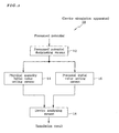
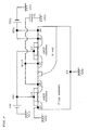
- FIG. 1 is a function block diagram showing a first embodiment of a device simulation apparatus related to the present invention. This drawing will be used for description as follows.
- a device simulation apparatus 10 of the present embodiment is to execute transient analysis on a device involving an exterior circuit. And, it comprises presumed potential designation means 12 for a user to designate a presumed potential in a first analysis bias of device electrode nodes; physical quantity initial value setting means 14 to acquire a physical quantity by analyzing the above described presumed potential as boundary conditions on a device, from which an external circuit has been removed, to set the above described physical quantity as the initial value of the physical quantity at the internal nodes in the device; potential initial value setting means 16 to set an initial value of potential at nodes of the external circuit based on already known potential and the above described presumed potential;, and device analyzing means 18 to analyze a device involving an external circuit with the above described respective initial values set by the physical quantity initial value setting means 14 and the potential initial value setting means 16.
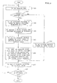
- FIG. 2 is a flow chart showing operation of the device simulation apparatus in FIG. 1. This drawing will be used for description as follows.
- a bias to be analyzed is set (Step 101).
- the bias to be analyzed is given as a set of values of a voltage source or a current source, and they are set one by one so that analysis is proceeded with.
- the bias to be analyzed is given as a set of values of a voltage source or a current source at a designated point of time, and the period sandwiched by those designated time point are divided appropriately so that biases corresponding to those time points are set for analysis to be proceeded with.
- a first bias of transient analysis that is, analysis on the bias at the time point zero to be executed is steady analysis.
- Step 102 it is checked whether or not the set analysis bias is a first analysis bias (Step 102).
- the state goes forward to Step 109 so that the result of analysis on the previous analysis bias is set as the initial value.
- the state goes forward to processing of Step 103 and onward.
- Step 103 the potential value which a user to execute analysis has presumed in advance is set.
- an initial state of the analysis is known.
- the initial state of the analysis is in a High state or a Low state, and it is in common to check how the state shifts to a Low state or a High state according to changes in the input bias. That is, it is possible for the user to presume potential of nodes on a device electrode.
- Step 104 Analysis of this device portion is analyzed with the coupled method or the Gammel method, which has been described in the section on analysis of the drift-diffusion model and the energy transportation model.
- Step 105 the resulting physical quantity given in Step 104, that is, the coulomb potential, the carrier density, and the carrier temperature, etc. is set as the initial value of physical quantity on the nodes inside the device.
- Step 106 the external circuit is traced from the nodes on the device electrodes to the ground (GND) nodes and an initial value of potential on external circuit nodes from the designated presumed potential designated at Step 103 and the voltage source potential is estimated and set (Step 106).
- This procedure corresponds with analysis only on the circuit equations of the external circuit portion with the electrode nodes as a fixed boundary.
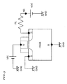
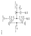
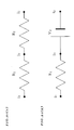
- Steps 103 to 106 so far will be described in an embodied fashion by taking as an example an nMOS inverter circuit of the resistant lode having been shown in FIG. 3.
- FIG. 3 shows a device involving an external circuit as a model.
- the circuit diagram expressed in a general illustrative method is expressed as in FIG. 4.
- An input terminal VIN, an output terminal VOUT and a power supply VCC in FIG. 4 correspond with the positive side node (G) of the voltage source VIN, the drain node (D) of the nMOS device, the positive node (NR) of the voltage source VCC in FIG. 3 respectively.
- Step 103 can be executed.
- the bias of nodes on the electrodes of the device portion can be given, and therefore with these as fixed boundary conditions, the device portion can be analyzed.
- the physical quantity of the analysis results is set as the initial value of the physical quantity of the device internal nodes. This is the process of Step 105.
- the presumed values of the potentials are given. These are set as the initial values of the device analysis involving the external circuit. This is the process of Step 106.
- Step 107 Since necessary initial values have been obtained with the processing up to Step 106 so far, subsequently analysis on the device involving an external circuit is executed. Here, due to availability of good initial values, the adoption of the coupled method makes it possible to execute analysis in shorter calculation time than with the Gammel method, and therefore the coupled method is used. This is the process of Step 107.
- Step 101 the process from Step 101 and onward will be executed.
- the process comes to an end. This is the process of Step 108.
- Step 109 the time ticking interval can be notched appropriately to a short extent in the case of transient analysis in particular, the solution for analysis of the subsequent analysis bias can be made available comparatively easily, and therefore for the initial values, the analysis results of the previous time will be used. This is the process of Step 109.
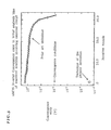
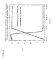
- a graph on convergence errors and iterative rounds of the initial analysis biases is shown in FIG. 5.
- the convergence condition for convergence error of coulomb potential is set at 10 -4 [V].
- the calculation time inclusive of the initial value setting process to obtain the solution of the initial analysis biases was 7.2 times longer than that in the technique of the present invention.
- the initial value setting according to the technique of the present invention is largely effective for shortening calculation time.
- the input waveform (chronological change in voltage of the voltage source VIN) and the output waveform (chronological change in voltage of the node D) of the analysis results of this example are shown in FIG. 6. Redundantly, the technique of the present invention as well as the prior art technique gives rise to the same calculation results within the range of convergence error.
- the present embodiment relates to the transient analysis on a CMOS inverter as a device involving an external circuit as shown as a model in FIG. 7.
- FIG. 7 which is expressed in a general illustrative method for a circuit, will be as in FIG. 8.
- An input terminal VIN, an output terminal VOUT and a power supply VDD in FIG. 8 correspond with the positive side node (NIN) of the voltage source VIN in FIG. 7, the node (NOUT) connecting the drain electrodes (DN, DP) of the nMOS transistor and pMOS transistor, the positive side node (NDD) of the voltage source VDD respectively.
- transient analysis when an input is changed to High from the state with a Low input VIN and a High output is considered.
- an analysis with the load capacitance CL being set at 0.1[pF] is considered by increasing the bias of VIN to 5.0[V] in 0.5[ns] with the initial analysis bias being 0.0[V] for the bias of input voltage source VIN and 5.0[v] for the VDD.
- Step 103 can be executed.
- the bias of nodes on the electrodes of the device portion can be given, and therefore with these as fixed boundary conditions, the device portion can be analyzed.
- the physical quantity of the analysis results is set as the initial value of the physical quantity of the device internal nodes.
- these nodes can be regarded as the potential fixed nodded, connections of the external circuit be traced up to the ground (GND) so that the potential of the external circuit connection point on the way can be guessed.
- NIN, NOUT, NDD are the nodes with potentials not yet fixed, and therefore, the circuit equations on these external circuit nodes should be established so that the solution may be given. That is, the following equations are solved.
- the initial analysis bias of transient analysis is an analysis at the time zero, which will be a steady analysis, connection with the load capacitance CL can be treated as being cut off. Accordingly, in the above described equations, no circuit equations on connection by the load capacitance CL appear.
- the presumed values of the potentials are given. These are set as the initial values of the device analysis involving the external circuit. This is the process of Step 106 of the present invention. Since the process described so far has availed necessary initial values, hereafter the device analysis involving an external circuit sill be executed as in the first embodiment so that the solution is given.
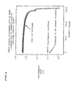
- FIG. 9 For the technique of the present invention and the prior art technique to set thermal balanced values as the initial value, a graph on convergence errors and iterative rounds of the initial analysis biases is shown in FIG. 9.
- the convergence condition for convergence error of coulomb potential is set at 10 -4 [V].
- the prior art technique 155 repetitions are required, but in the technique of the present invention, convergence takes place at one time.
- the calculation time inclusive of the initial value setting process to obtain the solution of the initial analysis biases was 25.6 times longer than that in the technique of the present invention.
- the initial value setting according to the technique of the present invention is largely effective for shortening calculation time.
- the input waveform (chronological change in voltage of the voltage source VIN) and the output waveform (chronological change in voltage of the node NOUT) of the analysis results of this example are shown in FIG. 10.
- FIG. 11 is a function block diagram showing a third embodiment of a device simulation apparatus related to the present invention. This drawing will be used for description as follows.
- a device simulation apparatus 20 of the present embodiment is to execute steady analysis on a device involving an exterior circuit. And, it comprises presumed potential designation means 22 for a user to designate presumed potentials in one or more analysis bias of device electrode nodes; physical quantity initial value setting means 24 to acquire a physical quantity by analyzing the above described presumed potential as boundary conditions on a device, from which an external circuit has been removed, to set the above described physical quantity as the initial value of the physical quantity at the internal nodes in the device; potential initial value setting means 26 to set an initial value of potential at nodes of the external circuit based on already known potential and the above described presumed potential;, and device analyzing means 28 to analyze a device involving an external circuit with the above described respective initial values set by the physical quantity initial value setting means 24 and the potential initial value setting means 26.
- FIG. 12 is a flow chart showing operation of the device simulation apparatus in FIG. 11. This drawing will be used for description as follows.
- the bias to be changed in the analysis is single is similar to the first embodiment. That is, as an analysis bias to execute the potential presuming process, an initial analysis bias is designated, and for the initial analysis bias in Step 202 a process of Steps 203 to 206 is executed. The contents of these processes are similar to those of the first embodiment. For the analysis bias other than the initial one, the process of Step 209 is executed. The contents of this process are similar to those in the first embodiment.
- the bias of the voltage source VIN is changed from 0[V] to 3.3[V]
- the bias of the voltage source VIN is changed from 0[V] to 5.0[V].
- Step 202 judges whether or not it is the designated analysis bias and in the case it is the designated analysis bias, as in case of the initial analysis bias, the initial values setting processes of Step 203 to 206 can be executed.
- a graph on convergence errors and iterative rounds of the analysis biases of 5.0[V] being the voltage source VDD and of 0[V] being the voltage source VIN is shown in FIG. 13.
- the convergence condition for convergence error of coulomb potential is set at 10 -4 [V].
- 177 repetitions are required, but in the technique of the present invention, convergence takes place at one time.
- the calculation time inclusive of the initial value setting process to obtain the solution of the initial analysis biases was 58.1 times longer than that in the technique of the present invention.
- the initial value setting according to the technique of the present invention is largely effective for shortening calculation time.
- FIG. 14 a graph on the relationship between the voltage of the voltage source VIN and the potential of the node NOUT being the analysis results of this example is shown in FIG. 14.
- initial values of physical quantity on the device internal node as well as external circuit node potential are given, and these are used as initial values for analysis so as to give appropriate initial values easily, and thus to be capable of shortening calculation time.
Landscapes
- Engineering & Computer Science (AREA)
- Physics & Mathematics (AREA)
- Theoretical Computer Science (AREA)
- Computer Hardware Design (AREA)
- Evolutionary Computation (AREA)
- Geometry (AREA)
- General Engineering & Computer Science (AREA)
- General Physics & Mathematics (AREA)
- Design And Manufacture Of Integrated Circuits (AREA)
- Metal-Oxide And Bipolar Metal-Oxide Semiconductor Integrated Circuits (AREA)
- Insulated Gate Type Field-Effect Transistor (AREA)
- Management, Administration, Business Operations System, And Electronic Commerce (AREA)
Applications Claiming Priority (2)
| Application Number | Priority Date | Filing Date | Title |
|---|---|---|---|
| JP2000122013 | 2000-04-24 | ||
| JP2000122013A JP2001308201A (ja) | 2000-04-24 | 2000-04-24 | 半導体デバイスシミュレーション装置及び方法並びにそのシミュレーションプログラムを記録した記録媒体 |
Publications (1)
| Publication Number | Publication Date |
|---|---|
| EP1150221A2 true EP1150221A2 (de) | 2001-10-31 |
Family
ID=18632548
Family Applications (1)
| Application Number | Title | Priority Date | Filing Date |
|---|---|---|---|
| EP01109783A Withdrawn EP1150221A2 (de) | 2000-04-24 | 2001-04-20 | Apparat zur Simulation von Halbleiterbauelementen, Verfahren und Speichermedium mit entsprechendem Simulationsprogramm |
Country Status (3)
| Country | Link |
|---|---|
| US (1) | US20020069041A1 (de) |
| EP (1) | EP1150221A2 (de) |
| JP (1) | JP2001308201A (de) |
Families Citing this family (3)
| Publication number | Priority date | Publication date | Assignee | Title |
|---|---|---|---|---|
| JP5416966B2 (ja) * | 2008-12-26 | 2014-02-12 | 株式会社東芝 | 半導体装置のシミュレーション装置 |
| JP2011199981A (ja) * | 2010-03-18 | 2011-10-06 | Ricoh Co Ltd | 信号送受信制御回路と2次電池保護回路 |
| CN113033128B (zh) * | 2021-03-29 | 2022-05-24 | 北京华大九天科技股份有限公司 | 一种选取电路仿真中牛顿迭代的初值的方法 |
-
2000
- 2000-04-24 JP JP2000122013A patent/JP2001308201A/ja not_active Withdrawn
-
2001
- 2001-04-12 US US09/834,053 patent/US20020069041A1/en not_active Abandoned
- 2001-04-20 EP EP01109783A patent/EP1150221A2/de not_active Withdrawn
Also Published As
| Publication number | Publication date |
|---|---|
| JP2001308201A (ja) | 2001-11-02 |
| US20020069041A1 (en) | 2002-06-06 |
Similar Documents
| Publication | Publication Date | Title |
|---|---|---|
| Newton | Techniques for the simulation of large-scale integrated circuits | |
| CN101341488B (zh) | 用于分析逻辑级的方法和系统 | |
| US8533644B1 (en) | Multi-CCC current source models and static timing analysis methods for integrated circuit designs | |
| Chen et al. | Verilog-A compatible recurrent neural network model for transient circuit simulation | |
| US20100031206A1 (en) | Method and technique for analogue circuit synthesis | |
| US20040078175A1 (en) | Method and apparatus for modeling and simulating the effects of bridge defects in integrated circuits | |
| US20050257077A1 (en) | Method for voltage drop analysis in integreted circuits | |
| Sadrossadat et al. | Nonlinear electronic/photonic component modeling using adjoint state-space dynamic neural network technique | |
| US7987439B2 (en) | Method and apparatus for analyzing circuit model by reduction and computer program product for analyzing the circuit model | |
| US6829755B2 (en) | Variable detail automatic invocation of transistor level timing for application specific integrated circuit static timing analysis | |
| EP0901088A2 (de) | Rahmenwerk zur Regel-Prüfung | |
| US6640330B1 (en) | System and method for setup and hold characterization in integrated circuit cells | |
| US5293327A (en) | Method of logic circuit simulation | |
| Nease et al. | Modeling and implementation of voltage-mode CMOS dendrites on a reconfigurable analog platform | |
| US6678869B2 (en) | Delay calculation method and design method of a semiconductor integrated circuit | |
| JPH06317631A (ja) | アナログ集積回路のための試験プランを発生する方法 | |
| Hou et al. | CONCERT: A concurrent transient fault simulator for nonlinear analog circuits | |
| CN114880975B (zh) | 一种硬件木马的生成方法、系统、设备以及介质 | |
| EP1150221A2 (de) | Apparat zur Simulation von Halbleiterbauelementen, Verfahren und Speichermedium mit entsprechendem Simulationsprogramm | |
| Bednar et al. | Stability of multi-rate simulation algorithms | |
| US5677848A (en) | Method to derive the functionality of a digital circuit from its mask layout | |
| Veetil et al. | Fast and accurate waveform analysis with current source models | |
| US8554529B2 (en) | Black box model for large signal transient integrated circuit simulation | |
| US20050080600A1 (en) | Mixed-signal finite state machine models ensuring analog continuity | |
| US9792392B2 (en) | Method for determining the sizing of the transistors of an analog circuit |
Legal Events
| Date | Code | Title | Description |
|---|---|---|---|
| PUAI | Public reference made under article 153(3) epc to a published international application that has entered the european phase |
Free format text: ORIGINAL CODE: 0009012 |
|
| AK | Designated contracting states |
Kind code of ref document: A2 Designated state(s): AT BE CH CY DE DK ES FI FR GB GR IE IT LI LU MC NL PT SE TR |
|
| AX | Request for extension of the european patent |
Free format text: AL;LT;LV;MK;RO;SI |
|
| RAP1 | Party data changed (applicant data changed or rights of an application transferred) |
Owner name: NEC ELECTRONICS CORPORATION |
|
| STAA | Information on the status of an ep patent application or granted ep patent |
Free format text: STATUS: THE APPLICATION HAS BEEN WITHDRAWN |
|
| 18W | Application withdrawn |
Effective date: 20040205 |