EP0901088A2 - Rahmenwerk zur Regel-Prüfung - Google Patents
Rahmenwerk zur Regel-Prüfung Download PDFInfo
- Publication number
- EP0901088A2 EP0901088A2 EP98306711A EP98306711A EP0901088A2 EP 0901088 A2 EP0901088 A2 EP 0901088A2 EP 98306711 A EP98306711 A EP 98306711A EP 98306711 A EP98306711 A EP 98306711A EP 0901088 A2 EP0901088 A2 EP 0901088A2
- Authority
- EP
- European Patent Office
- Prior art keywords
- structural
- node
- entities
- entity
- analysis
- Prior art date
- Legal status (The legal status is an assumption and is not a legal conclusion. Google has not performed a legal analysis and makes no representation as to the accuracy of the status listed.)
- Withdrawn
Links
Images
Classifications
-
- G—PHYSICS
- G06—COMPUTING OR CALCULATING; COUNTING
- G06F—ELECTRIC DIGITAL DATA PROCESSING
- G06F30/00—Computer-aided design [CAD]
- G06F30/30—Circuit design
- G06F30/36—Circuit design at the analogue level
- G06F30/367—Design verification, e.g. using simulation, simulation program with integrated circuit emphasis [SPICE], direct methods or relaxation methods
-
- G—PHYSICS
- G06—COMPUTING OR CALCULATING; COUNTING
- G06F—ELECTRIC DIGITAL DATA PROCESSING
- G06F30/00—Computer-aided design [CAD]
- G06F30/30—Circuit design
- G06F30/32—Circuit design at the digital level
- G06F30/33—Design verification, e.g. functional simulation or model checking
Definitions
- This invention relates generally to rules checking, and more particularly to a methodology of rules checking of a structure having one or more structural elements and one or more nodes that serve as connection points to the elements.
- a node may serve as an interconnection between two or more elements.
- one or more electrical elements may be connected by nodes that interconnect the electrical elements.
- a bridge is commonly made up of a number of wooden beams interconnected by bolts.
- a node may additionally be considered a connection point that connects an element to something else.
- a node may serve as a connection point to an external environment in which the structure is situated.
- a node may serve as an input or output point of an element.
- a node it is possible to have a structure having only one element and one node, two or more elements and one or more nodes, or one or more elements and two or more nodes, etc.
- Structural information is concerned with how elements and nodes interact with respect to one another.
- the structure of an element or node, or a group of elements and nodes can affect the behavior of other elements or nodes or groups of elements and nodes.
- Behavioral information is concerned with how elements and nodes, or groups of elements and nodes, react to stimuli to which they are subjected.
- the stimuli may be long term stimuli, as in the case of hot electrons in an electrical structure or rust in a mechanical structure, or short term stimuli, such as changes in voltage, temperature, or load conditions. For instance, the load condition of a bridge changes as a person drives across it; this change is temporary and is therefore a short term stimuli.
- Structural and behavioral information of the elements and nodes will of course vary according to the type of structure being analyzed. For instance, voltages and capacitances at various nodes of an electrical circuit are typically critical indicators of proper operation of the circuit. In the case of an electrical circuit, a netlist, or external representation of the circuit, simply specifies the physical interconnections or nodes between the electrical elements without providing information about various electrical parameters or measurements at those nodes. A netlist, then, is by itself insufficient to provide needed information about the nodes of an electrical circuit.
- a rules checking methodology analyzes a structure or system characterized as having one or more elements having one or more nodes as connection points to the elements.
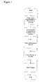
- the first step of the rules checking methodology of the present invention is to create an internal representation of the structure to be analyzed. Expected arrangements of the elements of the structure are found by searching for and extracting known topology types.
- an analysis of the elements and nodes of the structure is performed. All rules associated with a particular element or node of the structure are applied to the element or node in order to determine if that element or node meets certain criteria established for it.
- a report that illustrates the statistics compiled during the analysis of the structure elements and nodes is made available.
- Any structure to be analyzed may be characterized as having a number of structural elements that are interconnected by nodes or as having at least one structural element and at least one node that serves as a connection point to the structural element.
- the structure may be any number of things, including, but not limited to, an electronic circuit, a bridge or other civil engineering structure, and a mechanical transmission.
- Each of these examples of structures are characterized as having elements interconnected by nodes.
- a bridge is made of a number of support members, such as wooden beams, interconnected by nodes called bolts.
- the first step of the methodology of the present invention is to create an internal representation of the structure to be analyzed.
- the structure being analyzed may be an entire structure or system or it may simply be a subset of a larger structure or system.
- the rules checking methodology may be used to analyze an entire electrical system or it may be used to check only a portion of the entire electrical system, such as a circuit within the electrical system. In either case, what is being analyzed is referred to as the structure.
- the next step is to search for known and expected arrangements of elements of the structure in Block 20 by looking for and extracting known topology types. For instance, if the structure being analyzed is an electronic circuit then certain pathsets between electronic elements of the circuit would be expected to be seen. If there are problems in the pathset, this would be indicative of problems in the netlist, or external representation, of the electronic circuit. The problems in the netlist could then be corrected.
- Known topology types of an electronic circuit could include, but would not be limited to, static gate outputs, dynamic precharge nodes, dynamic gate inputs, block inputs, block outputs, and latches.
- the rules checking software of the present invention even allows the user to provide the software with hints, such as giving the software a list of the latch nodes, as will be described hereinafter in conjunction with Block 24 of Figure 2.
- information concerning the extraction of the topologies may be provided to the designer.
- Such information might contain a list of the assumptions used to find and extract the topologies. Further, the information might be a list of all of the topologies found and extracted. Based upon this information, the designer may make adjustments to the assumptions used to find and extract topologies or provide other hints to the rules checking software through the external information file described in Block 24 of Figure 2.
- an alternative to extracting topology types for the netlist of an electronic circuit is to blindly apply all the rules to each and every node and element of the electronic circuit.
- This approach makes developing the limits of the checks, to be discussed in greater detail with respect to Blocks 30 and 40, very difficult because the limits have to be set so that they are applicable to all elements and nodes of the structure.
- the parameters of a dynamic gate can be quite different from those used to check a static gate.
- Yet another alternative to extracting topology types is to rely on the structure designer to assign all the attributes to each and every element and node of the structure. This provides the advantage that the designer is aware of every assumption of the rules checking. However, this approach requires quite a bit of time of the designer and the person who enters all these rules into the rules checking code.
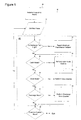
- Blocks 30 and 40 an analysis of the elements and nodes of the structure is performed.
- a check is performed on all elements of the structure in which all rules associated with a particular element are then applied to the element to determine if that element passes or fails certain criteria established for it. For instance, a load bearing beam element of a bridge may be expected to support X amount of weight and this rule is applied to the load bearing beam element to ascertain whether it meets this requirement.
- a check is performed on all the nodes that interconnect the elements of the structure being tested.
- a report that illustrates the statistics compiled during the analysis of the structure elements and nodes is made available in Block 50.
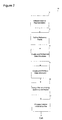
- Block 12 the internal representation of the structure to be analyzed is initialized by creating data structures that are used to track overhead information, such as the version of the database, the size of the database, the number of elements of the structure, the number of nodes of the structure, and the pointers of the structure.
- reference points of the structure are defined.
- a reference point is a connection point, or node, in the structure that must be known in order to adequately analyze the structure. For instance, in an electronic circuit structure, reference points might be ground and a power supply potential such as Vcc. In a bridge structure, a pylon might be a reference point that must be defined.
- a data structure is created for each element and data for each element is read into the data structure for that element.
- a data structure is created for each node and data for each node is read into the data structure for that node. It must be noted that the order of Blocks 16 and 18 could be reversed so that the node data structures are created prior to the element data structures, if desired.
- pointers among elements and nodes of the structure are assigned in the code of the program.
- preprocessing of an external information file is performed.
- the external information file provided by the user at Block 24 contains additional information about the structure that aids in the analysis of the structure. The additional information may be the result of analysis performed by external analysis tools or it may simply be hints provided by the designer to enhance the structural analysis.
- the external information file for example, may contain a list of the latch nodes and precharge nodes of an electrical circuit being analyzed.
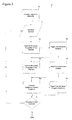
- Block 32 the loop of the elements of the structure are initialized.
- Block 34 an element to be analyzed is chosen.
- One or more properties of the element is then examined at Blocks 36-38.
- the properties to be examined may be structural properties, as in Block 36a, or behavioral properties, as in Block 37a. Examination of multiple properties of an element could be performed simultaneously, in parallel, if so desired to reduce the time associated with the examination of an element.
- Structural properties have to do with how elements and nodes interact with respect to one another.
- the structure of an element or node, or a group of elements and nodes can affect the behavior of other elements or nodes or groups of elements and nodes.
- a dimension of an element is an example of a structural property and may be any relevant characteristic of the element that is of particular concern. For instance, if the element is a transistor, such as a field effect transistor (FET), the dimension could be the gate width of the transistor. Or, if the element is a beam of a bridge, the dimension to be examined could be the cross-section of the beam or the material of the beam. As another example, consider the element to be a gear of a transmission, with the dimension being the thickness of the gear.
- FET field effect transistor
- the stimuli may be long term stimuli, as in the case of hot electrons in an electrical structure or rust in a mechanical structure, or short term stimuli, such as changes in voltage, temperature, or load conditions.
- Limits may be expressed in various forms well known in the art. Linear limits may be expressed as a lower limit, an upper limit, or within ⁇ a limit. For non-linear measurements, the use of polynomial coefficients and look-up tables may be used. Moreover, acceptable limits of a dimension may be set by the user of the invention to any desirable value. In the case of the beam of a bridge as the element, it may be that the cross-section of the beam must conform to one of four measurements.
- Block 37b If the beam being tested has a cross-section that falls outside the four acceptable measurements, the violation would be reported at Block 37b. Additional structural or behavior properties of an element are examined at Block 38a and any additional property violations are reported at Block 38b as shown. Finally, at Decision Block 39 the process is directed back to Block 34 if more elements are to be examined or returns back to Block 40 of the overall flow of Figure 1 if all elements to be analyzed have been examined.
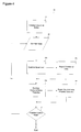
- Block 42 the loop of the nodes of the structure are initialized.
- Block 44 a node to be analyzed is chosen.
- the load or other property of the selected node is examined at Block 46a. If the load is not within acceptable limits, the violation is reported at Block 46b.
- Acceptable limits of a load may be set by the user of the invention to be any appropriate value. Consider, for instance, an electronic circuit example in which the voltage at a node is being measured. The acceptable value of voltage may be 5 ⁇ 0.5 volts.
- Block 46b If the voltage at the node being tested in less than 4.5 volts or greater than 5.5 volts, then the violation would be reported at Block 46b.
- Block 48a additional node properties are examined for a particular node and any additional property violations that may exist are reported at Block 48b.
- the process is directed back to Block 44 if more nodes are to be examined or returned to Block 50 of the overall flow of Figure 1 if all nodes to be analyzed have been examined.
- a word concerning node loads is appropriate here.
- a node load may be thought of as any measurable characteristic of concern at the node. For instance, in an electrical circuit the capacitance or voltage present at a particular node that interconnects electrical elements may be important to know. Similarly, the amplitude or frequency of a signal at the node in such a circuit may be critical. Or, in a bridge, the load-bearing properties of a fulcrum between two or more beams might be examined. In civil engineering endeavors, it is not uncommon to pre-load a beam in order to position it at a given location, and such pre-loaded beams are to be analyzed differently than other types of beams. Moreover, there are different types of nodes that may be examined. Consider a storage node. In an electric circuit, a storage node, such as a latch node, may store capacitance or voltage. In a mechanical system, the storage node may be a spring that stores energy. Storage nodes and precharge nodes are commonly found in electrical circuits.
- the examination of multiple properties or loads of a node could be performed simultaneously, in parallel, if so desired to reduce the time associated with the examination of a node. Additionally, examination of properties of one or more elements as shown in Figure 3 could be performed simultaneously to the examination of properties of one or more nodes of Figure 4.
- each processor may operate at the same time as any processor, but analysis of a particular element or node by a particular processor is completed before analysis of another element or node by the same processor may commence.
- the processor could be, but is not limited to, any electrical, mechanical or biological data processing unit such as a microprocessor, an electro-mechanical device, or a person.
- Decision Block 52 inquires about whether capacitance at the node being examined is within capacitance limits. If it is not, then violation of the acceptable capacitance for that particular node is reported at Block 54.
- Decision Blocks 56, 60, and 64 inquire about the type of node and then perform appropriate testing.
- Decision Block 56 inquires as to whether the node is a latch node. If the node being examined is a latch node, then latch node inquiries are performed at Block 58.
- Block 60 the question is whether the node is characterized as being a clock signal. If so, then inquiries about the clock signal are performed at Block 62. Finally, at Decision Block 64 the flow is directed to Block 66 for precharge node testing if the node is a precharge node.
- Blocks 52 to 64 could be performed in parallel to one another to reduce the run time required to complete node testing.
- the capacitance testing of Blocks 52 and 54 could be performed simultaneously with the latch node testing of Blocks 56 and 58 and the clock signal testing of Blocks 60 and 62.
- parallel testing could be employed in a system having, for instance, 10 microprocessor units, in order to test a structure having 1,000 or more nodes, with each processing unit simultaneously testing 100 different nodes of the structure.
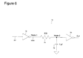
- Inverter 72 receives an input signal IN1 that is inverted to produce signal NIN1 at Node 1.
- Resistor 74 is valued at 200 Ohms while capacitor 76 is valued at 1 pF.
- the signal at Node 2 is provided to Inverter 78 where it is inverted to form output signal Out.
- the RC delay at Node 2 formed by the electrical connection of resistor 74, capacitor 76, and Inverter 78 is calculated by multiplying the resistance of resistor 74 by the capacitance of Node 2, represented by capacitor 76.
- the RC delay is 200 pS.
- the data structures of the elements, inverters 72, 78, and resistor 74, and the data structure of nodes Node 1 and Node 2 are created as illustrated by Blocks 16 and 18.
- the data structure created for an element or node may be the element or node itself, or it may be subelements that together define the element or node.
- inverter 72 The data structure for inverter 72 may be an inverter structure or it may be two field effect transistors that together equal an inverter.
- the resistance of 200 Ohms is data that is associated with the data structure of resistor 200; likewise, the capacitance of 1 pF is an attribute of Node 2 that fills the data structure of Node 2.
- the capacitance represented by capacitor 76 may or may not be considered a separate element of the circuit. In this case, the capacitance is not considered a separate element but is rather considered an attribute of Node 2.
- a search for known arrangements of the elements of the RC delay circuit is conducted.
- the elements and nodes of the RC delay circuit are analyzed.
- the critical part of the circuit is the RC delay at Node 2. So, referring to Blocks 46 and 47 the RC delay between Node 1 and Node 2 is examined. In this example, the RC delay between Node 1 and Node 2 is 200 pS. Now, suppose the acceptable upper limit is only 100 pS. Since the acceptable RC delay between Node 1 and Node 2 has been exceeded, this violation is reported at Block 47.
- the form of the violation report can take any form desired and may contain any important information.
- the error message could read as follows: "RC delay node: Node 2 rc_delay: 200pS limit: 100ps Failed_by_pct: 100.0 Finally, at Block 50 the statistics of RC delay circuit of Figure 6 are reported.
- the rules checking methodology of the present invention ensures the quality of a structure or system having one or more elements and one or more nodes that serve as connection points to the elements.
- the rules checking methodology examines the elements and nodes of the structure and makes decisions regarding the quality of the structure according to parameters provided by the structure designer.
- the parameters could include capacitance, resistance, and transistor size.
- extracted information from analyzing equipment such as timing analyzers, which provide slope, delay, and signal validity data, and automatic routers, which provide wire length data, may be used by the rules checking methodology of the present invention.
- Quality checks of an electronic circuit can be used to verify that the electronic circuit is immune to noise, temperature, voltage, and process variations.
- the rules checking methodology may also be used to perform existence checks for various types of properties such as checking a block input of a noise sensitive circuit.
Landscapes
- Engineering & Computer Science (AREA)
- Computer Hardware Design (AREA)
- Theoretical Computer Science (AREA)
- Physics & Mathematics (AREA)
- General Engineering & Computer Science (AREA)
- Geometry (AREA)
- Evolutionary Computation (AREA)
- General Physics & Mathematics (AREA)
- Microelectronics & Electronic Packaging (AREA)
- Design And Manufacture Of Integrated Circuits (AREA)
- Information Retrieval, Db Structures And Fs Structures Therefor (AREA)
- Testing Electric Properties And Detecting Electric Faults (AREA)
- Complex Calculations (AREA)
Applications Claiming Priority (2)
| Application Number | Priority Date | Filing Date | Title |
|---|---|---|---|
| US922793 | 1997-09-02 | ||
| US08/922,793 US5987237A (en) | 1997-09-02 | 1997-09-02 | Framework for rules checking |
Publications (2)
| Publication Number | Publication Date |
|---|---|
| EP0901088A2 true EP0901088A2 (de) | 1999-03-10 |
| EP0901088A3 EP0901088A3 (de) | 2002-03-20 |
Family
ID=25447583
Family Applications (1)
| Application Number | Title | Priority Date | Filing Date |
|---|---|---|---|
| EP98306711A Withdrawn EP0901088A3 (de) | 1997-09-02 | 1998-08-21 | Rahmenwerk zur Regel-Prüfung |
Country Status (3)
| Country | Link |
|---|---|
| US (1) | US5987237A (de) |
| EP (1) | EP0901088A3 (de) |
| JP (1) | JPH11149467A (de) |
Cited By (4)
| Publication number | Priority date | Publication date | Assignee | Title |
|---|---|---|---|---|
| FR2842001A1 (fr) * | 2002-04-02 | 2004-01-09 | Hewlett Packard Co | Procede et dispositif d'identification de situations de conflit dans une conception de circuit |
| WO2003021492A3 (en) * | 2001-08-29 | 2004-02-19 | Intel Corp | Simulating a logic design |
| WO2003021491A3 (en) * | 2001-08-29 | 2004-03-04 | Intel Corp | Real-time connection error checking method and process |
| EP1635274A4 (de) * | 2004-02-25 | 2006-11-02 | Matsushita Electric Industrial Co Ltd | Einrichtung und verfahren zur prüfung der stromquellenisolation bei leiterplatten |
Families Citing this family (14)
| Publication number | Priority date | Publication date | Assignee | Title |
|---|---|---|---|---|
| US6321365B1 (en) * | 1999-01-26 | 2001-11-20 | Hewlett-Packard Company | System and method for detecting storage nodes that are susceptible to charge sharing |
| US6701290B1 (en) * | 1999-02-18 | 2004-03-02 | Hewlett-Packard Development Company, L.P. | Method and apparatus for evaluating the design quality of network nodes |
| US7031889B1 (en) * | 1999-03-22 | 2006-04-18 | Hewlett-Packard Development Company, L.P. | Method and apparatus for evaluating the design quality of network nodes |
| US6367055B1 (en) * | 1999-04-27 | 2002-04-02 | Hewlett-Packard Company | Method and apparatus for determining certain characteristics of circuit elements |
| US6990643B1 (en) * | 1999-05-13 | 2006-01-24 | Hewlett-Packard Development Company, L.P. | Method and apparatus for determining whether an element in an integrated circuit is a feedback element |
| US6523152B1 (en) | 2000-03-08 | 2003-02-18 | Hewlett-Packard Company | Framework for rules checking utilizing resistor, nonresistor, node and small node data structures |
| US7082104B2 (en) | 2001-05-18 | 2006-07-25 | Intel Corporation | Network device switch |
| US7093224B2 (en) | 2001-08-28 | 2006-08-15 | Intel Corporation | Model-based logic design |
| US7130784B2 (en) | 2001-08-29 | 2006-10-31 | Intel Corporation | Logic simulation |
| US7073156B2 (en) | 2001-08-29 | 2006-07-04 | Intel Corporation | Gate estimation process and method |
| US6983427B2 (en) | 2001-08-29 | 2006-01-03 | Intel Corporation | Generating a logic design |
| US6859913B2 (en) | 2001-08-29 | 2005-02-22 | Intel Corporation | Representing a simulation model using a hardware configuration database |
| US7197724B2 (en) | 2002-01-17 | 2007-03-27 | Intel Corporation | Modeling a logic design |
| US7900178B2 (en) * | 2008-02-28 | 2011-03-01 | International Business Machines Corporation | Integrated circuit (IC) design method, system and program product |
Family Cites Families (8)
| Publication number | Priority date | Publication date | Assignee | Title |
|---|---|---|---|---|
| US4858146A (en) * | 1986-08-13 | 1989-08-15 | The Babcock & Wilcox Company | Automated design of structures using a finite element database |
| US5289567A (en) * | 1991-04-01 | 1994-02-22 | Digital Equipment Corporation | Computer apparatus and method for finite element identification in interactive modeling |
| JP2788820B2 (ja) * | 1991-08-30 | 1998-08-20 | 三菱電機株式会社 | シミュレーション装置 |
| US5394524A (en) * | 1992-08-07 | 1995-02-28 | International Business Machines Corporation | Method and apparatus for processing two graphics data streams in parallel |
| EP0600608B1 (de) * | 1992-10-29 | 1999-12-22 | Altera Corporation | Verfahren zum Prüfen von Entwürfen für programmierbare Logikschaltungen |
| US5522022A (en) * | 1993-11-24 | 1996-05-28 | Xerox Corporation | Analyzing an image showing a node-link structure |
| US5787274A (en) * | 1995-11-29 | 1998-07-28 | International Business Machines Corporation | Data mining method and system for generating a decision tree classifier for data records based on a minimum description length (MDL) and presorting of records |
| US5802508A (en) * | 1996-08-21 | 1998-09-01 | International Business Machines Corporation | Reasoning with rules in a multiple inheritance semantic network with exceptions |
-
1997
- 1997-09-02 US US08/922,793 patent/US5987237A/en not_active Expired - Fee Related
-
1998
- 1998-08-21 EP EP98306711A patent/EP0901088A3/de not_active Withdrawn
- 1998-08-31 JP JP10244774A patent/JPH11149467A/ja not_active Withdrawn
Cited By (5)
| Publication number | Priority date | Publication date | Assignee | Title |
|---|---|---|---|---|
| WO2003021492A3 (en) * | 2001-08-29 | 2004-02-19 | Intel Corp | Simulating a logic design |
| WO2003021491A3 (en) * | 2001-08-29 | 2004-03-04 | Intel Corp | Real-time connection error checking method and process |
| FR2842001A1 (fr) * | 2002-04-02 | 2004-01-09 | Hewlett Packard Co | Procede et dispositif d'identification de situations de conflit dans une conception de circuit |
| EP1635274A4 (de) * | 2004-02-25 | 2006-11-02 | Matsushita Electric Industrial Co Ltd | Einrichtung und verfahren zur prüfung der stromquellenisolation bei leiterplatten |
| US7489139B2 (en) | 2004-02-25 | 2009-02-10 | Panasonic Corporation | System and method for checking decoupling of power supply in printed wiring board |
Also Published As
| Publication number | Publication date |
|---|---|
| JPH11149467A (ja) | 1999-06-02 |
| EP0901088A3 (de) | 2002-03-20 |
| US5987237A (en) | 1999-11-16 |
Similar Documents
| Publication | Publication Date | Title |
|---|---|---|
| US5987237A (en) | Framework for rules checking | |
| US5446676A (en) | Transistor-level timing and power simulator and power analyzer | |
| US6311147B1 (en) | Integrated circuit power net analysis | |
| US6314546B1 (en) | Interconnect capacitive effects estimation | |
| Ju et al. | Incremental techniques for the identification of statically sensitizable critical paths | |
| US6675118B2 (en) | System and method of determining the noise sensitivity characterization for an unknown circuit | |
| US6748572B2 (en) | Power supply network analyzing method, computer program for executing the method, storage medium and power supply network analyzing apparatus | |
| US6993470B2 (en) | Method of evaluating test cases in a simulation environment by harvesting | |
| US8468478B2 (en) | Methods for measurement and prediction of hold-time and exceeding hold time limits due to cells with tied input pins | |
| US6763504B2 (en) | Method for reducing RC parasitics in interconnect networks of an integrated circuit | |
| US6587815B1 (en) | Windowing scheme for analyzing noise from multiple sources | |
| Burks et al. | Min-max linear programming and the timing analysis of digital circuits | |
| US7082587B2 (en) | Method of estimating path delays in an IC | |
| US6470479B1 (en) | Method of verifying semiconductor integrated circuit reliability and cell library database | |
| US5369604A (en) | Test plan generation for analog integrated circuits | |
| US6560571B1 (en) | Method and apparatus for prioritizing the order in which checks are performed on a node in an integrated circuit | |
| US6550041B1 (en) | Method and apparatus for evaluating the design quality of network nodes | |
| Damiano et al. | Checking satisfiability of a conjunction of BDDs | |
| US6389578B1 (en) | Method and apparatus for determining the strengths and weaknesses of paths in an integrated circuit | |
| US7587305B2 (en) | Transistor level verilog | |
| US6367055B1 (en) | Method and apparatus for determining certain characteristics of circuit elements | |
| US6321365B1 (en) | System and method for detecting storage nodes that are susceptible to charge sharing | |
| US6523152B1 (en) | Framework for rules checking utilizing resistor, nonresistor, node and small node data structures | |
| US7006931B2 (en) | System and method for efficient analysis of transmission lines | |
| US6990643B1 (en) | Method and apparatus for determining whether an element in an integrated circuit is a feedback element |
Legal Events
| Date | Code | Title | Description |
|---|---|---|---|
| PUAI | Public reference made under article 153(3) epc to a published international application that has entered the european phase |
Free format text: ORIGINAL CODE: 0009012 |
|
| AK | Designated contracting states |
Kind code of ref document: A2 Designated state(s): AT BE CH CY DE DK ES FI FR GB GR IE IT LI LU MC NL PT SE Kind code of ref document: A2 Designated state(s): DE FR GB |
|
| AX | Request for extension of the european patent |
Free format text: AL;LT;LV;MK;RO;SI |
|
| RAP1 | Party data changed (applicant data changed or rights of an application transferred) |
Owner name: HEWLETT-PACKARD COMPANY, A DELAWARE CORPORATION |
|
| PUAL | Search report despatched |
Free format text: ORIGINAL CODE: 0009013 |
|
| AK | Designated contracting states |
Kind code of ref document: A3 Designated state(s): AT BE CH CY DE DK ES FI FR GB GR IE IT LI LU MC NL PT SE |
|
| AX | Request for extension of the european patent |
Free format text: AL;LT;LV;MK;RO;SI |
|
| 17P | Request for examination filed |
Effective date: 20020531 |
|
| AKX | Designation fees paid |
Free format text: DE FR GB |
|
| 17Q | First examination report despatched |
Effective date: 20041216 |
|
| STAA | Information on the status of an ep patent application or granted ep patent |
Free format text: STATUS: THE APPLICATION IS DEEMED TO BE WITHDRAWN |
|
| 18D | Application deemed to be withdrawn |
Effective date: 20060304 |