EP1150127A2 - Verfahren zur Bestimmung einer Einzellösung der Parameter eines FET-Schaltungsmodells - Google Patents
Verfahren zur Bestimmung einer Einzellösung der Parameter eines FET-Schaltungsmodells Download PDFInfo
- Publication number
- EP1150127A2 EP1150127A2 EP01110452A EP01110452A EP1150127A2 EP 1150127 A2 EP1150127 A2 EP 1150127A2 EP 01110452 A EP01110452 A EP 01110452A EP 01110452 A EP01110452 A EP 01110452A EP 1150127 A2 EP1150127 A2 EP 1150127A2
- Authority
- EP
- European Patent Office
- Prior art keywords
- parameters
- fet
- model
- equivalent circuit
- parameter values
- Prior art date
- Legal status (The legal status is an assumption and is not a legal conclusion. Google has not performed a legal analysis and makes no representation as to the accuracy of the status listed.)
- Withdrawn
Links
Images





Classifications
-
- G—PHYSICS
- G06—COMPUTING OR CALCULATING; COUNTING
- G06Q—INFORMATION AND COMMUNICATION TECHNOLOGY [ICT] SPECIALLY ADAPTED FOR ADMINISTRATIVE, COMMERCIAL, FINANCIAL, MANAGERIAL OR SUPERVISORY PURPOSES; SYSTEMS OR METHODS SPECIALLY ADAPTED FOR ADMINISTRATIVE, COMMERCIAL, FINANCIAL, MANAGERIAL OR SUPERVISORY PURPOSES, NOT OTHERWISE PROVIDED FOR
- G06Q50/00—Information and communication technology [ICT] specially adapted for implementation of business processes of specific business sectors, e.g. utilities or tourism
- G06Q50/04—Manufacturing
-
- G—PHYSICS
- G01—MEASURING; TESTING
- G01R—MEASURING ELECTRIC VARIABLES; MEASURING MAGNETIC VARIABLES
- G01R31/00—Arrangements for testing electric properties; Arrangements for locating electric faults; Arrangements for electrical testing characterised by what is being tested not provided for elsewhere
- G01R31/26—Testing of individual semiconductor devices
- G01R31/2607—Circuits therefor
- G01R31/2621—Circuits therefor for testing field effect transistors, i.e. FET's
-
- G—PHYSICS
- G06—COMPUTING OR CALCULATING; COUNTING
- G06F—ELECTRIC DIGITAL DATA PROCESSING
- G06F30/00—Computer-aided design [CAD]
- G06F30/30—Circuit design
- G06F30/36—Circuit design at the analogue level
- G06F30/367—Design verification, e.g. using simulation, simulation program with integrated circuit emphasis [SPICE], direct methods or relaxation methods
Definitions
- the present invention relates generally to the field of high frequency small signal analysis and more specifically to a modeling method for extracting a single set of equivalent circuit model parameters that specifically simulate measured S-parameters, but are also useful in the development of non-linear Field Effect Transistor (FET) models, and analysis of the physical structure of the FET.
- FET Field Effect Transistor
- Non-unique models consist of parameters that are not physically consistent with the FETs fabrication parameters, such as layout dimensions and material parameters.
- the cold-FET based model extraction methods do not express the bias-dependence of parasitic elements correctly.
- the present invention provides a FET modeling algorithm that generates a unique solution for FET feedback impedance, thus determining resistive, capacitive, and inductive equivalent circuit parameter values based on a single set of S-parameter measured values.
- the subsequent extracted circuit model is a unique global solution rather than a non-unique local minima.
- the extracted values satisfy self-consistent checks such as scaling with FET device periphery, expected bias-dependence, and convergence to known fabrication parameters such as gate metalization resistance, material sheet resistance, gate length and recess dimensions.
- the method includes the step of competitive extraction where multiple trial solutions are attempted spanning a region or "space" of feedback impedance values. Each solution in the competitive extraction can be achieved by utilizing the same cycle of conventional direct extraction via Minasian extraction.
- the extraction step is followed by an optimization step that reduces the extracted values to a model that better fits measured S-parameters. This optimization step can be achieved by conventional optimization algorithms.
- selection of the most accurate and unique trial solution can be achieved by further evaluating the speed of convergences in an error metric.
- Also disclosed is a method for unique determination of FET equivalent circuit parameter values comprising the steps of selecting a feedback impedance value from a space of expected parameter values and generating a FET equivalent circuit model.
- the method further includes the step of establishing those parameter values for the circuit model that converge fastest so that a sufficiently low error fit between the expected S-parameters and the measured S-parameter is obtained, the convergence obtained using multiple Minasian extraction and optimization cycles.
- a technical advantage of the invention is that by tracking the speed of convergence, the solutions surrounding unique, physically significant models condense faster than the rest. Conventional techniques stop once some least-squares based error metric is minimized.
- Another technical advantage of the invention is the development of unique models that best represents the physical structure of a FET. This has been proven through extensive verification and testing.
- the present invention is a unique and novel method of extracting both intrinsic and parasitic equivalent circuit parameter values for a FET device (not shown). This capability is vital for the generation of accurate high-frequency nonlinear FET circuit models. Accurate bias dependent and linear equivalent circuits are not only important to circuit design, but are also needed to provide a close description of the physical structure of a device for process feedback.
- the description of the invention is presented in connection with the small signal circuit model upon which the extraction method of the present invention has been used to extract feedback resistance values between the gate, source and drain terminals of the circuit model.
- a process flow diagram illustrating the competitive extraction method of the invention is shown and described with reference to a specific example.
- a set of plots are presented for various circuit model parameters such as the source resistance (R s ), the gate-to-source capacitance (C GS ), the transconductance (G M ), the gate-source, gate-drain line capacitance (C GS , C DG ) and the percentage error in the gate source line capacitances as a function of gate-source voltage (V GS ) and total device periphery.
- the plots are evidence of convergence between a set of measured device parameter values and extracted parameter values so that the error between the two values sets is minimized.
- Figure 1 is a process flow diagram of a method, denoted generally as 100, of determining unique FET parameter values of a FET device (not shown).
- the method uses S-parameters which are measured on the FET device as well as S-parameters calculated from a circuit model to determine the parameters of the FET device.
- the present invention provides a method of extracting realistic parameter values for the circuit model 200 that accurately reflect the FET device modeled by the circuit 200.
- the method 100 will be described with reference to a specific example.
- the method 100 begins at step 102 wherein a circuit model which is representative a FET device is generated.
- a circuit model which is representative a FET device is generated.
- FIG 2 therein is shown an example equivalent circuit model of a FET device, denoted generally as 200, on which the extraction algorithm of the present invention can be applied to extract a unique set of circuit parameter values.
- the topology of circuit model 200 is complete enough to model most FET small-signal characteristics in all bias regimes.
- the circuit model 200 includes gate 202, drain 204 and source206 terminals with an assortment of resistance, impedance and capacitance parameters extending between the gate 202, drain 204, and source 206 terminals. These parameters include the source resistance R S , the gate-source capacitance C GS , and the transconductance G M , among others as indicated in the figure.
- the circuit model 200 represents an ideal FET device suitable for demonstration of the ability to uniquely and accurately determine the FET feedback impedance through a single set of measured S-parameter values
- the circuit model 200 a designer will consider the operating frequency and bias condition of the FET device to be modeled as carriers enter the device through the source 206 and leave through the drain 204 subject to the control or gating action of the gate terminal 202.
- the voltages applied to the gate relative to the source can determine the operating region of the device as V GS is increased from zero to a threshold voltage level (V T ) that biases the device into its active region.
- V T threshold voltage level
- the model 200 contains circuit parameters and components, designated as Rs, Ls, Rg, Lg, Rd and Ld.
- the selection of the initial inductance (L), resistance (R), transconductance (G) and capacitance (C) values for the various components of the circuit model 200 is straightforward when it is assumed the performance of the underlying device is linear with frequency. (Such assumptions, however, prove inaccurate for most FET device models since most are non-linear at high frequencies and given actual device profiles peripheries. This assumption however does provide an initial starting point for the method of the present invention).
- the next step in the process is to measure the S-parameters for the FET device, step 104. To do so, the FET device is physically tested and measured and the S-parameters for the FET device are determined. A determination is then made as to whether the measurements and the associated measured S-parameter values are accurate, step 106. To do so requires the knowledge of one skilled in the art. If the parameters are not accurate, the S-parameters are remeasured until the measurements are acceptable.
- Figures 3 and 4 show visual examples of measured FET S-parameters for a selected FET device. Note that four S-parameter measurements are shown in which three are depicted in a Smith Chart format ( Figure 3) and one is shown in a linear graph format ( Figure 4). Assuming the measured S-parameters are accurate, the measured S-parameters are stored, step 108, for use during subsequent comparison.
- the space defining all values for trial feedback impedance solutions is generated, step 110.
- the trail feedback impedance space could be as shown in Table 1.
- the trial values are used to generate a set of feedback resistance values or points.
- the points can be thought of as extending from one (1) to N, where N is in the Nth trial feedback impedance solution in the space generated at step 110.
- step 112 is to extract model parameters for each point, N, in the feedback impedance space generated at step 110.
- the extractions are preferably achieved by utilizing Minasian extraction algorithms which are known in the art.
- step 118 is to compare the measured S-parameters to the modeled S-parameters.
- an initial guess at the model solution is made for the initial parasitic values. This initial guess is an informed guess made by one skilled in the art.
- An example of an initial guess for the parasitic circuit parameters Rs, Lg, Rs, Ls, Rd and Rd, for model circuit 200 are shown in Table 3. The intrinsic and extrinsic values are applied to the circuit model and the S-parameters are calculated for the model circuit.
- the intrinsic values shown in Tables 2 and 3 as well as the values for Rs and Ls for each impedance point, N shown in Table 1, is applied to the circuit model 200 and the S-parameters are calculated for each impedance point, N, preferably using a Minasian extraction algorithm mentioned above.
- step 118 is to compare the calculated S-parameters to the measured S-parameters for each impedance point, N, where the measured S-parameters were stored in step 108.
- the measured values for the S11, S12 and S22 parameters are depicted by the curves identified by the squares, circles and inverted diamonds, respectively.
- the simulated or modeled values for S11, S12 and S22 are depicted by the lines marked by the triangles, diamonds and stars, respectively.
- the next step in the process, step 122, is to select a test parameter criteria and determine if that criteria has been met.
- the test parameter criteria can be selected amount of time or a selected number of runs.
- the selected criteria will be the same for each trial value.
- the preselected criteria is preferably a preselected number of cycles of the extraction-optimization routine indicated by the box marked 121.
- the feedback resistance value which starts off closest to the unique solution will contain the least amount of error and converge faster and obtain a low best fit value quicker.
- the preselected criteria was completion of six (6) extraction-optimization cycles where one cycle is depicted by the subroutine indicated by reference number 121.
- step 122 is to optimize the model parameters.
- known optimization programs are used.
- a commercially available computer program, Libra 3.5, produced by HP EEsof could be used as the optimizer program.
- the optimization is additionally performed per preselected restrictions.
- the optimization program Libra 3.5 could be used with the restrictions shown in Table 4 for a fixed value of Rs. These constraints are in accordance with the overall modeling algorithm.
- the optimization of the model parameters is confined to creating a trial model solution for only the trial feedback impedance point, Rs.
- the optimized values for the equivalent circuit parameters are output from the optimization program.
- Tables 5 and 6 show example optimized equivalent circuit parameters for the circuit 200 ( Figure 2), are output from the Libra 3.5 computer program.
- Rs is a fixed value for the cycles.
- Implementation Parameter Circuit Simulator and Optimizer Libra 3.5 Optimization Algorithm Gradient Optimization Error Metric Mag and angle of S11,S21,S12,and S22 from 4 to 40 GHz Number of Iterations 60 Number of Extraction/Optimization Cycles 6 Optimized "Intrinsic" equivalent circuit parameters.
- Intrinsic Equivalent Circuit Parameter Initial Solution Cgs 0.227785 pF Rgs 65247 ⁇ Cgd 0.017016 pF Rgd 130820 ⁇ Cds 0.047521 pF Rds 160.18 ⁇ Gm 135.74 mS Tau 0.446 pS Optimized "Parasitic" equivalent circuit parameters.
- Intrinsic Equivalent Circuit Parameter Initial Solution Rg 4.715 ⁇ Lg 0.02903 nH Rs 1.7 ⁇ Ls 0.002102 nH Rd 3.2893 ⁇ Ld 0.0317 nH
- step 112 These new optimized parameters are input into step 112 and the process is repeated.
- the steps 112-122 are repeated until the preselected criteria is met at step 120 for each trial solution point.
- the modeled values more closely match with the measured values.
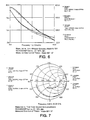
- Figures 7 and 8 visually depict a comparison of the measured and simulated S-parameter values after six (6) extraction-optimization cycles 121 for the circuit model 200 of Figure 2.
- Figures 7 and 8 are compared to Figures 4 and 5, respectively, it can be seen that the measured and modeled values converge with application of the process 100.
- the next step in the process is to form a new error metric, step 124.
- the final error and convergence speed for each of the trial solution points are compared to determine which trial solution produced the lowest final error.
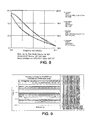
- the graph of Figure 9 shows the final fitting error for the circuit model 200 as a function of Rs, where Rs is plotted along the horizontal axis with the appropriate scaling factors for fitting the error indicated along the vertical axis. Not that a final fitting error is generated for each trail solution point, N.
- the next step in the process is to select the model solution which resulted in the minimal error in the new error metric, step 126. Since each trial solution point was subjected to the same preselected criteria, for example, six (6) cycles at step 120, the implementation of the extraction-optimization cycles results in the best and the fastest solving model solution appear as the global minima, depicted by reference number 127, for the final fitting errors of all trial impedance points. For the example depicted by the graph of Figure 9, the minima 127 occurs for an Rs value of approximately 1.7 ohms. The minima 127 in final error indicates that the algorithm of the present invention converges to a unique solution as opposed to conventional algorithms which would produce near flat dependencies or local minima solutions which do not usually obey device scaling realities. Thus, with unique solutions for the feedback resistance, the rest of the equivalent circuit model 200 can be uniquely determined.
- the next step in the process is to output the circuit parameters corresponding to the selected model solution.
- These circuit parameters were calculated at step 112 for the last cycle of process 121.
- step 126 an accurate model of the FET device that is unique is obtained at step 128.
- Intrinsic Equivalent Circuit Parameter Initial Solution Cgs 0.227745 pF Rgs 64242 ⁇ Cgd 0.017019 pF Rgd 133450 ⁇ Cds 0.047544 pF Rds 160.1791 ⁇ Gm 135.7568 mS Tau 0.443867 pS Global solution "Parasitic" equivalent circuit parameters.
- Intrinsic Equivalent Circuit Parameter Initial Solution Rg 4.711895 ⁇ Lg 0.029314 nH Rs 1.7 ⁇ Ls 0.002104 nH Rd 3.309899 ⁇ Ld 0.031671 nH
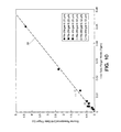
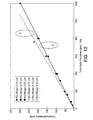
- Figure 10 is a plot of the source resistance as a function of gate width (W G ) in 2-finger, 4-finger and 8-finger FET configurations. For all configurations, the source resistance R S follows roughly the dashed line 70 indicating a direct dependence with 1/W G as would be expected.
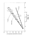
- FIG 11 illustrates a plot of the gate source capacitance C GS (indicated along the vertical axis) as a function of 1/W G .
- the extracted values for C GS are plotted for both a 0.25 ⁇ m (indicated by the oval A) and a 0.12 ⁇ m GaAs pseudomorphic High Electron Mobility Transistor (HEMT, indicated by the oval B).
- the lines surrounding each device model are indicated from top to bottom as 2, 4, and 8-finger configurations with unit gate periphery indicated along the horizontal axis.
- C GS follows a direct dependence with the total gate width periphery W G for the extracted values.
- Figure 12 is a plot of the transconductance G M as a function of total gate periphery W G .
- the extracted values are shown for G M scaled for both in a 0.12 mm (oval A) and a 0.25 mm GaAs pseudomorphic HEMT (oval B).
- the transconductance G M follows a direct dependence with the total gate with W G as expected.
- circuit models can be extracted with physically significant parameters and subtle Physics-based phenomena in FETs can be observed from measured bias dependent S-parameters.
- the expected gate metal resistance could be determined from well-known scaling rules.
- Figure 13 is a plot of the source resistance R s versus the gate bias voltage V GS plotted along the horizontal axis.
- the extraction of both parasitic and intrinsic equivalent circuit parameter values provide a close view of the physical structure of the device.
- the lateral extension of the space-charge region and the modulation of surface state density in the recess can be observed in the bias dependence of R s vs. V GS .
- C GS and C GD The bias dependence of C GS and C GD is typical of HEMTs as confirmed by the reports of many researchers. This bias dependence is illustrated in the bias plot of Figure 14.
- C GS and C GD are equal and then gradually C GS increases while C GD decreases as the FET is biased into its linear region.
- C GS follows a hyperbolic tangent-like function in saturation with a sharp increase occurring near pinch-off voltage and then saturating to a peak value.
- Increasing C GS as V GS moves positive is indicative of charge spilling out of the channel and into the donor or Schottky Barrier layer, amounting to an effect sometimes called parasitic conduction.
- DIBL Drain-Induced-Barrier-Lowering
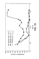
- Figure 15 is a plot showing a percentage error in the gate-source capacitance C GS as a function of the gate source voltage V GS .
- Figure 16 illustrates percent error in the scaled gate-source capacitance C GS versus scaled device periphery W G , as indicated along the horizontal axis.
- constant parasitic assumptions become more inaccurate when the FET is biased with V GS approaching pinch-off and as V DS decreases into the linear region.
- small errors in the fitting of the equivalent circuit caused by assuming constant parasitics with bias are greatly magnified as the device model is scaled. Roughly, a 10% error/ 20 ⁇ m of device scaling occurs simply because the intrinsic model of the original device started with a small error.
Landscapes
- Engineering & Computer Science (AREA)
- Computer Hardware Design (AREA)
- Physics & Mathematics (AREA)
- Theoretical Computer Science (AREA)
- General Physics & Mathematics (AREA)
- Microelectronics & Electronic Packaging (AREA)
- Business, Economics & Management (AREA)
- Evolutionary Computation (AREA)
- Geometry (AREA)
- General Engineering & Computer Science (AREA)
- Marketing (AREA)
- Health & Medical Sciences (AREA)
- Economics (AREA)
- General Health & Medical Sciences (AREA)
- Human Resources & Organizations (AREA)
- Manufacturing & Machinery (AREA)
- Primary Health Care (AREA)
- Strategic Management (AREA)
- Tourism & Hospitality (AREA)
- General Business, Economics & Management (AREA)
- Measurement Of Resistance Or Impedance (AREA)
- Testing Of Individual Semiconductor Devices (AREA)
- Testing Or Measuring Of Semiconductors Or The Like (AREA)
Applications Claiming Priority (4)
| Application Number | Priority Date | Filing Date | Title |
|---|---|---|---|
| US20043600P | 2000-04-28 | 2000-04-28 | |
| US200436P | 2000-04-28 | ||
| US680339 | 2000-10-05 | ||
| US09/680,339 US6594594B1 (en) | 2000-04-28 | 2000-10-05 | Method for unique determination of FET equivalent circuit model parameters |
Publications (2)
| Publication Number | Publication Date |
|---|---|
| EP1150127A2 true EP1150127A2 (de) | 2001-10-31 |
| EP1150127A3 EP1150127A3 (de) | 2006-01-25 |
Family
ID=26895760
Family Applications (1)
| Application Number | Title | Priority Date | Filing Date |
|---|---|---|---|
| EP01110452A Withdrawn EP1150127A3 (de) | 2000-04-28 | 2001-04-27 | Verfahren zur Bestimmung einer Einzellösung der Parameter eines FET-Schaltungsmodells |
Country Status (4)
| Country | Link |
|---|---|
| US (1) | US6594594B1 (de) |
| EP (1) | EP1150127A3 (de) |
| JP (1) | JP3437959B2 (de) |
| KR (1) | KR100413214B1 (de) |
Cited By (3)
| Publication number | Priority date | Publication date | Assignee | Title |
|---|---|---|---|---|
| CN106202627A (zh) * | 2016-06-23 | 2016-12-07 | 南京展芯通讯科技有限公司 | 包含本征电感的晶体管小信号等效电路模型及参数提取方法 |
| CN110717241A (zh) * | 2019-08-27 | 2020-01-21 | 西安电子科技大学 | 一种InP HEMT小信号等效电路模型及其参数提取方法 |
| CN117556770A (zh) * | 2024-01-12 | 2024-02-13 | 华南理工大学 | 一种新型GaN HEMT晶体管高频噪声等效电路模型 |
Families Citing this family (12)
| Publication number | Priority date | Publication date | Assignee | Title |
|---|---|---|---|---|
| TW522246B (en) * | 2001-11-20 | 2003-03-01 | Yung-Ling Lai | Method of using discrete capacitance transmission line model to extract parasitic capacitance of field effect transistor |
| US20040002844A1 (en) * | 2002-06-27 | 2004-01-01 | Jess Jochen A.G. | System and method for statistical modeling and statistical timing analysis of integrated circuits |
| US6691285B1 (en) * | 2002-08-27 | 2004-02-10 | Hewlett-Packard Development Company, L.P. | Exponential increments in FET size selection |
| JP4608179B2 (ja) * | 2002-12-20 | 2011-01-05 | ルネサスエレクトロニクス株式会社 | Mosfetの等価回路モデルの容量パラメータ算出方法 |
| US20050183048A1 (en) * | 2004-01-30 | 2005-08-18 | Harald Kinzelbach | Method to simulate the influence of production-caused variations on electrical interconnect properties of semiconductor layouts |
| KR100716798B1 (ko) | 2005-12-29 | 2007-05-14 | 전자부품연구원 | 고주파용 디바이스의 모델링 방법 |
| JP4946131B2 (ja) * | 2006-03-29 | 2012-06-06 | 横河電機株式会社 | 燃料電池の特性測定装置及び方法 |
| US7741857B2 (en) * | 2008-03-06 | 2010-06-22 | International Business Machines Corporation | System and method for de-embedding a device under test employing a parametrized netlist |
| US8010930B2 (en) * | 2008-12-29 | 2011-08-30 | International Business Machine Corporation | Extracting consistent compact model parameters for related devices |
| US9164159B2 (en) * | 2012-12-14 | 2015-10-20 | Apple Inc. | Methods for validating radio-frequency test stations |
| US9772391B2 (en) * | 2014-01-24 | 2017-09-26 | Tektronix, Inc. | Method for probe equalization |
| CN109884490B (zh) * | 2019-01-09 | 2021-02-12 | 惠科股份有限公司 | 一种薄膜晶体管的检测方法和检测装置 |
Family Cites Families (1)
| Publication number | Priority date | Publication date | Assignee | Title |
|---|---|---|---|---|
| US5467291A (en) * | 1991-09-09 | 1995-11-14 | Hewlett-Packard Company | Measurement-based system for modeling and simulation of active semiconductor devices over an extended operating frequency range |
-
2000
- 2000-10-05 US US09/680,339 patent/US6594594B1/en not_active Expired - Fee Related
-
2001
- 2001-02-23 JP JP2001047656A patent/JP3437959B2/ja not_active Expired - Fee Related
- 2001-03-06 KR KR10-2001-0011549A patent/KR100413214B1/ko not_active Expired - Fee Related
- 2001-04-27 EP EP01110452A patent/EP1150127A3/de not_active Withdrawn
Cited By (6)
| Publication number | Priority date | Publication date | Assignee | Title |
|---|---|---|---|---|
| CN106202627A (zh) * | 2016-06-23 | 2016-12-07 | 南京展芯通讯科技有限公司 | 包含本征电感的晶体管小信号等效电路模型及参数提取方法 |
| CN106202627B (zh) * | 2016-06-23 | 2023-09-22 | 南京展芯通讯科技有限公司 | 包含本征电感的晶体管小信号等效电路模型及参数提取方法 |
| CN110717241A (zh) * | 2019-08-27 | 2020-01-21 | 西安电子科技大学 | 一种InP HEMT小信号等效电路模型及其参数提取方法 |
| CN110717241B (zh) * | 2019-08-27 | 2021-07-16 | 西安电子科技大学 | 一种InP HEMT小信号等效电路模型及其参数提取方法 |
| CN117556770A (zh) * | 2024-01-12 | 2024-02-13 | 华南理工大学 | 一种新型GaN HEMT晶体管高频噪声等效电路模型 |
| CN117556770B (zh) * | 2024-01-12 | 2024-05-07 | 华南理工大学 | 一种新型GaN HEMT晶体管高频噪声等效电路模型 |
Also Published As
| Publication number | Publication date |
|---|---|
| US6594594B1 (en) | 2003-07-15 |
| JP2001318118A (ja) | 2001-11-16 |
| JP3437959B2 (ja) | 2003-08-18 |
| KR20010098396A (ko) | 2001-11-08 |
| KR100413214B1 (ko) | 2003-12-31 |
| EP1150127A3 (de) | 2006-01-25 |
Similar Documents
| Publication | Publication Date | Title |
|---|---|---|
| US6594594B1 (en) | Method for unique determination of FET equivalent circuit model parameters | |
| US20180307789A1 (en) | STATISTICAL ANALYSIS METHOD FOR TECHNOLOGICAL PARAMETERS OF GaN DEVICES BASED ON LARGE-SIGNAL EQUIVALENT CIRCUIT MODEL | |
| US6711723B2 (en) | Hybrid semi-physical and data fitting HEMT modeling approach for large signal and non-linear microwave/millimeter wave circuit CAD | |
| CN106202835A (zh) | 包含沟道高级寄生元件的场效应晶体管小信号等效电路模型 | |
| JP2004501509A6 (ja) | ハイブリッド非線形大信号のマイクロ波/ミリ波モデル | |
| Jarndal et al. | A new small signal model parameter extraction method applied to GaN devices | |
| US20020116691A1 (en) | Semi-physical modeling of HEMT high frequency noise equivalent circuit models | |
| EP0997833A2 (de) | Grosssignalmodell für einen pseudomorphischen Heteroübergang-Transistor mit Elektronenbeweglichkeit | |
| US20020055193A1 (en) | Process perturbation to measured-modeled method for semiconductor device technology modeling | |
| CN106909741A (zh) | 一种微波GaN功率器件的建模方法 | |
| KR20020093961A (ko) | Hemt 고주파수 소 신호 등가 회로 모델의 반 물리적모델링 | |
| CN120087313B (zh) | 一种GaN HEMT器件等效电路模型的参数提取方法 | |
| US6573744B2 (en) | S-parameter microscopy for semiconductor devices | |
| Pengg | Direct parameter extraction on RF-CMOS | |
| US20020073387A1 (en) | Embedding parasitic model for pi-fet layouts | |
| Chiang et al. | Inverse modeling of two-dimensional MOSFET dopant profile via capacitance of the source/drain gated diode | |
| Cojocaru et al. | Parasitic resistance extraction errors with implications for FET model accuracy around V/sub ds/= 0 | |
| KR20020093959A (ko) | Hemt 고주파수 잡음 등가 회로 모델의 반-물리적 모델링 | |
| CN121435915A (zh) | 仿真模型的建模方法、存储介质和终端 | |
| JPH06215059A (ja) | 回路シミュレーション方法及びその装置 | |
| WO2001084600A1 (en) | Process perturbation to measured-modeled method for semiconductor device technology modeling | |
| JPH11202021A (ja) | 半導体評価装置、半導体評価方法、および半導体評価プログラムを記録したコンピュータ読み取り可能な記録媒体 | |
| Luo et al. | Modeling the Virtual Gate Voltage in Dispersive GaN HEMTs | |
| JP2001119017A (ja) | モデルパラメータ抽出方法およびその方式 | |
| Debie et al. | Fast and accurate on-wafer extraction of parasitic resistances in GaAs MESFET's |
Legal Events
| Date | Code | Title | Description |
|---|---|---|---|
| PUAI | Public reference made under article 153(3) epc to a published international application that has entered the european phase |
Free format text: ORIGINAL CODE: 0009012 |
|
| AK | Designated contracting states |
Kind code of ref document: A2 Designated state(s): AT BE CH CY DE DK ES FI FR GB GR IE IT LI LU MC NL PT SE TR |
|
| AX | Request for extension of the european patent |
Free format text: AL;LT;LV;MK;RO;SI |
|
| RAP1 | Party data changed (applicant data changed or rights of an application transferred) |
Owner name: NORTHROP GRUMMAN CORPORATION |
|
| RAP1 | Party data changed (applicant data changed or rights of an application transferred) |
Owner name: NORTHROP GRUMMAN CORPORATION |
|
| PUAL | Search report despatched |
Free format text: ORIGINAL CODE: 0009013 |
|
| RIC1 | Information provided on ipc code assigned before grant |
Ipc: G06F 17/50 19950101ALI20051124BHEP Ipc: G01R 31/26 19680901AFI20010803BHEP |
|
| AK | Designated contracting states |
Kind code of ref document: A3 Designated state(s): AT BE CH CY DE DK ES FI FR GB GR IE IT LI LU MC NL PT SE TR |
|
| AX | Request for extension of the european patent |
Extension state: AL LT LV MK RO SI |
|
| STAA | Information on the status of an ep patent application or granted ep patent |
Free format text: STATUS: THE APPLICATION IS DEEMED TO BE WITHDRAWN |
|
| 18D | Application deemed to be withdrawn |
Effective date: 20051101 |