EP1143774A2 - Wiring board comprising granular magnetic film - Google Patents
Wiring board comprising granular magnetic film Download PDFInfo
- Publication number
- EP1143774A2 EP1143774A2 EP01108515A EP01108515A EP1143774A2 EP 1143774 A2 EP1143774 A2 EP 1143774A2 EP 01108515 A EP01108515 A EP 01108515A EP 01108515 A EP01108515 A EP 01108515A EP 1143774 A2 EP1143774 A2 EP 1143774A2
- Authority
- EP
- European Patent Office
- Prior art keywords
- wiring board
- magnetic
- board according
- loss material
- magnetic loss
- Prior art date
- Legal status (The legal status is an assumption and is not a legal conclusion. Google has not performed a legal analysis and makes no representation as to the accuracy of the status listed.)
- Granted
Links
Images



Classifications
-
- H—ELECTRICITY
- H05—ELECTRIC TECHNIQUES NOT OTHERWISE PROVIDED FOR
- H05K—PRINTED CIRCUITS; CASINGS OR CONSTRUCTIONAL DETAILS OF ELECTRIC APPARATUS; MANUFACTURE OF ASSEMBLAGES OF ELECTRICAL COMPONENTS
- H05K1/00—Printed circuits
- H05K1/02—Details
-
- H—ELECTRICITY
- H05—ELECTRIC TECHNIQUES NOT OTHERWISE PROVIDED FOR
- H05K—PRINTED CIRCUITS; CASINGS OR CONSTRUCTIONAL DETAILS OF ELECTRIC APPARATUS; MANUFACTURE OF ASSEMBLAGES OF ELECTRICAL COMPONENTS
- H05K3/00—Apparatus or processes for manufacturing printed circuits
- H05K3/22—Secondary treatment of printed circuits
- H05K3/24—Reinforcing of the conductive pattern
- H05K3/244—Finish plating of conductors, especially of copper conductors, e.g. for pads or lands
-
- H—ELECTRICITY
- H05—ELECTRIC TECHNIQUES NOT OTHERWISE PROVIDED FOR
- H05K—PRINTED CIRCUITS; CASINGS OR CONSTRUCTIONAL DETAILS OF ELECTRIC APPARATUS; MANUFACTURE OF ASSEMBLAGES OF ELECTRICAL COMPONENTS
- H05K1/00—Printed circuits
- H05K1/02—Details
- H05K1/0213—Electrical arrangements not otherwise provided for
- H05K1/0216—Reduction of cross-talk, noise or electromagnetic interference
- H05K1/023—Reduction of cross-talk, noise or electromagnetic interference using auxiliary mounted passive components or auxiliary substances
- H05K1/0233—Filters, inductors or a magnetic substance
Definitions
- the inventors having previously invented a composite magnetic body exhibiting large magnetic loss at high frequencies, discovered a method wherewith, by deploying that composite magnetic body in the vicinity of a spurious radiation source, the generation of spurious radiation from the semiconductor devices and electronic circuits noted earlier, etc., is effectively suppressed.
- the size of the equivalent resistance component is dependent on the size of the magnetic loss factor ⁇ '' of the magnetic body. More specifically, the size of the resistance component that is equivalently inserted in an electronic circuit is roughly proportional to ⁇ " and the thickness of the magnetic body when the area of the magnetic body is constant. Accordingly, a larger ⁇ " becomes necessary in order to obtain a desired spurious radiation attenuation with a smaller or thinner magnetic body.
- M-X-Y compositions where M is a magnetic metal element, Y is either O, N, or F, and X is an element other than M or Y
- M-X-Y granular magnetic bodies the size of the saturation magnetization is dependent on the volume ratio accounted for by the M component. Therefore, the ratio of the M component must be made high to obtain large saturation magnetization.
- the inventors studied the ratio of the M component in granular magnetic bodies having the M-X-Y composition (where M is a magnetic metal element, Y is either O, N, or F, and X is an element other than M or Y) across a wide range, and discovered, as a result, that, with every composition system, large magnetic loss is exhibited in high-frequency regions when the magnetic metal M is present within a specific concentration range.
- the frequency dispersion width for the magnetic loss factor ⁇ " will become narrow, wherefore such materials are suitable for anti-noise measures in narrow-band frequency ranges.
- the electrical resistivity will be even larger, at roughly 500 ⁇ cm or greater, so the loss due to eddy currents will be extremely small, and, because the magnetic interaction between M component becomes small, spin thermal disturbance becomes large, and quivering develops in the frequency where natural resonance occurs.
- the magnetic loss factor ⁇ " will come to exhibit a large value across a broad range. Accordingly, this composition region is suitable for wide-band high-frequency current suppression.
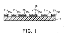
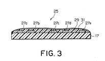
- a flexible wiring board 25 according to a second embodiment of the present invention is like a conventional flexible wiring board in that conductor patterns 27a, 27b, 27c, 27d, and 27e of copper or other conductive metal are deployed on the flexible base material 17 of a polyimide or the like.
- an insulation layer 25 which consists of a synthetic resin or the like so as to cover the entire surface on the side where the conductor patterns 27a, 27b, 27c, 27d, and 27e are deployed, inclusive of the conductor patterns 27a, 27b, 27c, 27d, and 27e, and on the surface of that insulation layer 25 is formed a granular magnetic thin film 31, by vapor deposition or the like, across the entirety thereof. If necessary, moreover, such can be formed in one part only.
- a resin or the like other than a polyimide can be used for the base material of the wiring board so long as it is a synthetic resin exhibiting insulating properties and flexibility.
- the fifth printed wiring board 61 consisting of a glass epoxy material is formed.
- the conductor patterns 67 are formed, and on top of those, the granular magnetic thin films 65 are formed. Further, also on the surface where no conductor patterns 67 are formed, the granular magnetic thin films 65 are formed, at intervals with the conductor patterns 67.
- the granular magnetic thin films 65 deployed between the conductor patterns can be deployed directly on the insulation board and used as conductors even if not deployed so as to make contact on the conductor patterns 67.
- the multi-layer wiring board according to the third embodiment is configured such that, after applying the first and third printed wiring boards 55 and 57, the second, fourth, and fifth printed wiring boards or insulation layers are formed in order.
- multiple printed wiring boards having a glass epoxy material as the board may be prepared from the beginning, and those applied using an adhesive such as an epoxy resin or the like.
- a multi-layer wiring board 69 has first to fifth printed wiring boards 55, 53, 57, 59, and 61, having a polyimide as their base material, formed in laminar fashion.
- the second printed wiring board 53 deployed below the first printed wiring board 55 comprises a ground pattern 63 on one surface thereof, and a conductor pattern 67 on the other surface thereof.
- On the ground pattern of the second printed wiring board 53 is formed a granular magnetic thin film 65 across the entire surface thereof.
- granular magnetic thin films 65 are formed, and thereupon is stacked one surface side of the first printed wiring board 55.
- the third and fourth printed wiring boards 57 and 59 each having conductor patterns 67 on one side thereof. On those conductor patterns 67 are formed granular magnetic thin films 65.
- the fifth printed wiring board 61 On the surface of the fourth printed wiring board 59 on which the conductor patterns 67 are formed is formed the fifth printed wiring board 61.
- An insulation film 71 is formed so as to cover the entire surface of the surface where the conductor patterns 67 on the outer surface of the fifth printed wiring board 61 are formed, and the granular magnetic thin film 65 is formed so as to cover the entire surface thereon.
- the high-frequency waves emitted from the conductor patterns 67 are absorbed by the granular magnetic thin films 65, and converted to heat, wherefore the emission of high-frequency noise from the multi-layer wiring board to the outside can be suppressed.
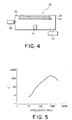
- a granular magnetic thin film was fabricated on the glass board 77 by sputtering, under the conditions noted below in Table 2.
- the sputtered film obtained thereby was subjected to a heat treatment in a vacuum magnetic field for 2 hours at 300°C to yield sample 2.
- the composition of the film was found to be Fe 72 Al 11 O 17 .
- the film thickness in sample 2 was 2.0 ⁇ m
- the DC resistivity was 530 ⁇ cm
- Hk was 18 Oe (1422 A/m)
- Ms was 16800 Gauss (1.68 T)
- the relative bandwidth bwr was 148%.
- Comparative sample 2 was obtained by the same method and under the same conditions as sample 2 except in that the number of Al 2 O 3 chips was made 90.
- unilayer or multilayer wiring boards can be provided that have magnetic thin films which exhibit outstanding high-frequency magnetic loss characteristics that are extremely useful in eliminating interference caused by spurious electromagnetic emissions or electromagnetic noise in unilayer or multilayer wiring boards that use high frequencies.
Landscapes
- Engineering & Computer Science (AREA)
- Microelectronics & Electronic Packaging (AREA)
- Physics & Mathematics (AREA)
- Electromagnetism (AREA)
- Manufacturing & Machinery (AREA)
- Thin Magnetic Films (AREA)
- Shielding Devices Or Components To Electric Or Magnetic Fields (AREA)
- Parts Printed On Printed Circuit Boards (AREA)
- Hard Magnetic Materials (AREA)
Abstract
Description
| Vacuum Degree before Deposition | <1 x 10⁻⁶ Torr (= 1.33 x 10⁻⁴ Pa) |
| Oxygen Flow Rate upon Deposition | 3.0 sccm |
| Material | Fe70Al30 alloy |
| Vacuum Degree before Deposition | < 1 x 10⁻⁶ Torr (= 1.33 x 10⁻⁴ Pa) |
| Atmosphere upon Deposition | Ar |
| Power Supply | RF |
| Target | Fe (⊘ 100mm) Al2O3 chip (120 pieces) (chip size: 5mm x 5mm x 2mmt) |
| Permeability Characteristics | ||
| Granular Magnetic Thin Film | Composite Magnetic Sheet | |
| µ "/700MHz | about 1800 | about 3.0 |
| bwr(%) | 148 | 196 |
Claims (39)
- A wiring board comprising:an insulative base material;conductor patterns formed thereon; andmagnetic thin films formed on said conductor pattern.
- The wiring board according to claim 1, wherein said magnetic thin films are formed on said conductor patterns along outer surfaces of said conductor patterns.
- The wiring board according to claim 1, wherein said magnetic thin films are formed with an insulation layer interposed therebetween, that covers entirety of surface of said wiring board on which said conductor patterns are formed.
- The wiring board according to claim 2, wherein said base material is configured of a flexible material.
- The wiring board according to claim 4, wherein said flexible material is a polyimide.
- The wiring board according to claim 1, wherein said magnetic thin films are produced by at least one of sputtering and vapor deposition.
- The wiring board according to claim 1, wherein thickness of said magnetic thin films is within range of 0.3 µm to 20 µm.
- The wiring board according to claim 1, wherein said magnetic thin film is configured of a magnetic loss material having a composition represented by M-X-Y, where M is at least one of Fe, Co, and Ni, X is at least one element other than M or Y, and Y is at least one of F, N, and O,said magnetic loss material is a narrow-band magnetic loss material in which a maximum value µ"max of loss factor µ" that is imaginary component in complex permeability characteristic of said magnetic loss material exists within a frequency range of 100 MHz to 10 GHz, anda relative bandwidth bwr is not greater than 200% where the relative bandwidth bwr is obtained by extracting a frequency bandwidth between two frequencies at which the value of µ" is 50% of the maximum µ "max and normalizing the frequency bandwidth at the center frequency thereof.
- The wiring board according to claim 8, wherein X component of said magnetic loss material is at least one of C, B, Si, Al, Mg, Ti, Zn, Hf, Sr, Nb, Ta, and rare earth elements.
- The wiring board according to claim 8, wherein, in said magnetic loss material, said M exists in a granular form dispersed in matrix of said X-Y compound.
- The wiring board according to claim 8, wherein mean particle diameter of particles M having said granular form is within range of 1 nm to 40 nm.
- The wiring board according to claim 8, wherein said magnetic loss material exhibits an anisotropic magnetic field Hk of 600 Oe (4.74 × 10⁴ A/m) or less.
- The wiring board according to claim 8, wherein said magnetic loss material is selected from Feα-Alβ-Oγ and Feα-Siβ-Oγ.
- The wiring board according to claim 8, wherein size of saturation magnetization in said magnetic loss material is within a range of 80% to 60% of saturation magnetization of a metal magnetic body consisting solely of M component.
- The wiring board according to claim 8, wherein said magnetic loss material exhibits a DC electrical resistivity that is within a range of 100 µΩ·cm to 700 µΩ·cm.
- The wiring board according to claim 1, wherein said magnetic thin film is configured of a magnetic loss material having a composition represented by M-X-Y, where M is at least one of Fe, Co, and Ni, X is at least one element other than M or Y, and Y is at least one of F, N, and O,said magnetic loss material is a broad-band magnetic loss material in which maximum value µ"max of loss factor µ" that is imaginary component in complex permeability characteristic of said magnetic loss material exists within a frequency range of 100 MHz to 10 GHz, anda relative bandwidth bwr is not smaller than 150% where the relative bandwidth bwr is obtained by extracting a frequency bandwidth between two frequencies at which the value of µ" is 50% of the maximum µ "max and normalizing the frequency bandwidth at the center frequency thereof.
- The wiring board according to claim 16, wherein size of saturation magnetization of said magnetic loss material is within range of 60% to 35% of saturation magnetization of a metal magnetic body consisting solely of M component.
- The wiring board according to claim 16, wherein said magnetic loss material exhibits a DC electrical resistivity having a value larger than 500 µΩ·cm.
- A wiring board comprising:a board of at least one layer comprising a conductor part; andmagnetic thin films deployed at least on part of said board or said conductor part.
- The wiring board according to claim 19, wherein said conductor part has a ground part that is either a ground surface or that comprises ground patterns deployed on one surface of said board, and entire surface of said ground part is covered with a magnetic thin film.
- The wiring board according to claim 19, wherein said conductor part comprises at least one of ground patterns or conductor patterns deployed on one surface of said board, or comprises a ground surface deployed over entirety of one surface of said board, and at least part of said conductor part is formed by an electrically conductive magnetic thin film.
- The wiring board according to claim 19, wherein said conductor part comprises signal line conductor patterns.
- The wiring board according to claim 22, wherein said magnetic thin film is formed on said signal line conductor patterns.
- The wiring board according to claim 22, wherein said magnetic thin films are formed so as to be separated from signal line conductor patterns in portion where said signal line conductor patterns are not formed.
- The wiring board according to claim 22, wherein said magnetic thin film is deployed with an insulation layer interposed therebetween so as to cover said conductor patterns.
- The wiring board according to claim 22, wherein said magnetic thin film is fabricated by at least one method of sputtering and vapor deposition.
- The wiring board according to claim 22, wherein said magnetic thin film has a thickness within a range of 0.3 µm to 20 µm.
- The wiring board according to claim 22, wherein said wiring board is a multilayer printed wiring board comprising a structure of at least 3 layers.
- The wiring board according to claim 22, whereinsaid magnetic thin film is configured of a magnetic loss material represented by M-X-Y, where M is at least one of Fe, Co, and Ni, Y is at least one of F, N, and O, and X is at least one element other than M or Y,said magnetic loss material is a broad-band magnetic loss material in which maximum value µ"max of loss factor µ" that is imaginary component in complex permeability of said magnetic loss material exists within a frequency range of 100 MHz to 10 GHz, anda relative bandwidth bwr is not smaller than 150% where the relative bandwidth bwr is obtained by extracting a frequency bandwidth between two frequencies at which the value of µ " is 50% of the maximum µ "max and normalizing the frequency bandwidth at the center frequency thereof.
- The wiring board according to claim 29, wherein size of saturation magnetization in said magnetic loss material is within a range of 60% to 35% of saturation magnetization of a metal magnetic body consisting solely of M component.
- The wiring board according to claim 19, wherein said magnetic loss material exhibits a DC electrical resistivity having a value larger than 500 µΩ·cm.
- The wiring board according to claim 22, wherein said magnetic thin film is configured of a magnetic loss material having a composition represented by M-X-Y, where M is at least one of Fe, Co, and Ni, Y is at least one of F, N, and O, and X is at least one element other than M or Y,said magnetic loss material is a narrow-band magnetic loss material in which maximum value µ"max of loss factor µ" that is imaginary component in complex permeability of said magnetic loss material exists within a frequency range of 100 MHz to 10 GHz, anda relative bandwidth bwr is not greater than 200% where the relative bandwidth bwr is obtained by extracting a frequency bandwidth between two frequencies at which the value of µ " is 50% of the maximum µ "max and normalizing the frequency bandwidth at the center frequency thereof.
- The wiring board according to claim 32, wherein size of saturation magnetization in said magnetic loss material is within a range of 80% to 60% of saturation magnetization of a metal magnetic body consisting solely of M component.
- The wiring board according to claim 32, wherein said magnetic loss material exhibits a DC electrical resistivity that is within a range of 100 µΩ·cm to 700 µΩ·cm.
- The wiring board according to claim 32, wherein X component of said magnetic thin film is at least one of C, B, Si, Al, Mg, Ti, Zn, Hf, Sr, Nb, Ta, and rare earth elements.
- The wiring board according to claim 32, wherein, in said magnetic loss material, said M exists in a granular form dispersed in matrix of said X-Y compound.
- The wiring board according to claim 32, wherein mean particle diameter of particles M having said granular form is within range of 1 nm to 40 nm.
- The wiring board according to claim 32, wherein said magnetic loss material exhibits an anisotropic magnetic field Hk of 600 Oe (5.34 x 10⁴ A/m) or less.
- The wiring board according to claim 32, wherein said magnetic loss material is selected from Feα-Alβ-Oγ and Feα-Siβ-Oγ.
Applications Claiming Priority (4)
| Application Number | Priority Date | Filing Date | Title |
|---|---|---|---|
| JP2000101765 | 2000-04-04 | ||
| JP2000101756 | 2000-04-04 | ||
| JP2000101765A JP4417521B2 (en) | 2000-04-04 | 2000-04-04 | Wiring board |
| JP2000101756A JP2001284755A (en) | 2000-04-04 | 2000-04-04 | Wiring board |
Publications (3)
| Publication Number | Publication Date |
|---|---|
| EP1143774A2 true EP1143774A2 (en) | 2001-10-10 |
| EP1143774A3 EP1143774A3 (en) | 2002-02-27 |
| EP1143774B1 EP1143774B1 (en) | 2004-01-14 |
Family
ID=26589399
Family Applications (1)
| Application Number | Title | Priority Date | Filing Date |
|---|---|---|---|
| EP01108515A Expired - Lifetime EP1143774B1 (en) | 2000-04-04 | 2001-04-04 | Wiring board comprising granular magnetic film |
Country Status (9)
| Country | Link |
|---|---|
| US (4) | US6653573B2 (en) |
| EP (1) | EP1143774B1 (en) |
| KR (1) | KR100882388B1 (en) |
| CN (1) | CN100336423C (en) |
| DE (1) | DE60101756T2 (en) |
| MY (1) | MY126823A (en) |
| NO (1) | NO20011707L (en) |
| SG (1) | SG100666A1 (en) |
| TW (1) | TWI268125B (en) |
Cited By (1)
| Publication number | Priority date | Publication date | Assignee | Title |
|---|---|---|---|---|
| EP2048919A4 (en) * | 2006-06-30 | 2010-01-06 | Shinetsu Polymer Co | Noise suppressing wiring member and printed wiring board |
Families Citing this family (16)
| Publication number | Priority date | Publication date | Assignee | Title |
|---|---|---|---|---|
| MY131112A (en) * | 2000-04-04 | 2007-07-31 | Nec Tokin Corp | Electromagnetic noise suppressor, semiconductor device using the same, and method of manufacturing the same |
| JP2002064189A (en) * | 2000-08-21 | 2002-02-28 | Tokin Corp | Magnetic random access memory |
| US7371471B2 (en) * | 2004-03-08 | 2008-05-13 | Nec Tokin Corporation | Electromagnetic noise suppressing thin film |
| JP4701942B2 (en) * | 2005-09-14 | 2011-06-15 | Tdk株式会社 | Module with built-in semiconductor IC |
| DE102007055291A1 (en) * | 2006-11-22 | 2008-06-26 | Nec Tokin Corp., Sendai | Multilayered printed circuit board useful in semiconductor device, comprises an internal magnetic layer, an internal conductive layer, a dielectric layer, a signal layer formed on the dielectric layer, and a cable bushing |
| JP5139750B2 (en) * | 2006-11-22 | 2013-02-06 | Necトーキン株式会社 | Multilayer printed circuit board |
| TWI382645B (en) * | 2006-12-29 | 2013-01-11 | Hon Hai Prec Ind Co Ltd | Power supply apparatus |
| JP5082060B2 (en) * | 2008-05-22 | 2012-11-28 | 学校法人明星学苑 | Low characteristic impedance power supply / ground pair line structure |
| JP6079425B2 (en) * | 2012-05-16 | 2017-02-15 | 日立化成株式会社 | Conductive particles, anisotropic conductive adhesive film, and connection structure |
| US9307631B2 (en) * | 2013-01-25 | 2016-04-05 | Laird Technologies, Inc. | Cavity resonance reduction and/or shielding structures including frequency selective surfaces |
| US20160029477A1 (en) * | 2013-02-27 | 2016-01-28 | Nec Corporation | Wiring substrate, semiconductor device, printed board, and method for producing wiring substrate |
| US10212806B2 (en) * | 2017-01-09 | 2019-02-19 | Laird Technologies, Inc. | Absorber assemblies having a dielectric spacer, and corresponding methods of assembly |
| CN110035603B (en) * | 2019-04-25 | 2021-08-03 | 电子科技大学 | A kind of preparation method of printed circuit embedded inductor |
| TWI756155B (en) * | 2021-07-19 | 2022-02-21 | 長春石油化學股份有限公司 | Surface-treated copper foil and copper clad laminate |
| US12101873B2 (en) | 2022-04-25 | 2024-09-24 | Microsoft Technology Licensing, Llc | Flexible printed circuit cable assembly with electromagnetic shielding |
| CN119300251B (en) * | 2024-12-13 | 2025-07-11 | 嘉兴明瑞电子科技有限公司 | PCB board and preparation method thereof |
Family Cites Families (27)
| Publication number | Priority date | Publication date | Assignee | Title |
|---|---|---|---|---|
| JPS531468B2 (en) | 1972-08-30 | 1978-01-19 | ||
| JPH01151297A (en) | 1987-12-08 | 1989-06-14 | Nec Corp | Composite circuit substrate |
| JPH01235662A (en) * | 1988-03-16 | 1989-09-20 | Hitachi Ltd | Recording electrode and manufacture thereof |
| JP2799465B2 (en) | 1989-10-04 | 1998-09-17 | イビデン株式会社 | Magnetic alloy layer coated circuit board |
| EP0422760A1 (en) | 1989-10-12 | 1991-04-17 | Mitsubishi Rayon Co., Ltd | Amorphous alloy and process for preparation thereof |
| JPH04196285A (en) | 1990-11-27 | 1992-07-16 | Ibiden Co Ltd | Metal layer coating circuit board |
| JPH05183291A (en) | 1991-12-27 | 1993-07-23 | Japan Metals & Chem Co Ltd | Manufacture of emi shield printed wiring board |
| JPH06275927A (en) | 1993-03-19 | 1994-09-30 | Cmk Corp | Printed wiring board having magnetic field-electromagnetic wave shield layer and manufacture thereof |
| JPH0758485A (en) | 1993-08-20 | 1995-03-03 | Cmk Corp | Printed wiring board having magnetic field / electromagnetic wave shield layer and manufacturing method thereof |
| JP2665134B2 (en) * | 1993-09-03 | 1997-10-22 | 日本黒鉛工業株式会社 | Flexible circuit board and method of manufacturing the same |
| US5639989A (en) * | 1994-04-19 | 1997-06-17 | Motorola Inc. | Shielded electronic component assembly and method for making the same |
| US5738931A (en) * | 1994-09-16 | 1998-04-14 | Kabushiki Kaisha Toshiba | Electronic device and magnetic device |
| JPH08250858A (en) | 1995-03-07 | 1996-09-27 | Ngk Spark Plug Co Ltd | Circuit board |
| US5698131A (en) * | 1995-05-15 | 1997-12-16 | Matsushita Electric Industrial Co., Ltd. | Paste for manufacturing ferrite and ferrite |
| JP3327375B2 (en) * | 1996-04-26 | 2002-09-24 | 富士通株式会社 | Magnetoresistive transducer, method of manufacturing the same, and magnetic recording apparatus |
| JP3151155B2 (en) * | 1996-09-10 | 2001-04-03 | アルプス電気株式会社 | Thin film magnetic head |
| JPH10105961A (en) * | 1996-09-26 | 1998-04-24 | Mitsubishi Chem Corp | Magnetic recording medium, recording and reproducing method thereof, and magnetic recording device |
| JP3184465B2 (en) * | 1996-11-19 | 2001-07-09 | アルプス電気株式会社 | Thin film magnetic head and method of manufacturing the same |
| JP2867985B2 (en) * | 1996-12-20 | 1999-03-10 | 日本電気株式会社 | Printed circuit board |
| JPH1196520A (en) * | 1997-09-17 | 1999-04-09 | Fujitsu Ltd | Magnetic head, method of manufacturing the same, and magnetic recording apparatus provided with the magnetic head |
| JPH11233909A (en) | 1998-02-18 | 1999-08-27 | Kyocera Corp | Wiring board |
| US5998048A (en) * | 1998-03-02 | 1999-12-07 | Lucent Technologies Inc. | Article comprising anisotropic Co-Fe-Cr-N soft magnetic thin films |
| JPH11274362A (en) | 1998-03-25 | 1999-10-08 | Kyocera Corp | Wiring board |
| JP3769120B2 (en) * | 1998-05-08 | 2006-04-19 | 株式会社東芝 | Semiconductor element |
| JP3474455B2 (en) * | 1998-09-10 | 2003-12-08 | Tdk株式会社 | Thin film magnetic head and method of manufacturing the same |
| US6021050A (en) * | 1998-12-02 | 2000-02-01 | Bourns, Inc. | Printed circuit boards with integrated passive components and method for making same |
| US6462630B1 (en) * | 2000-07-03 | 2002-10-08 | Oki Electric Cable Co., Ltd. | Wideband noise reducing device |
-
2001
- 2001-04-03 SG SG200101997A patent/SG100666A1/en unknown
- 2001-04-03 US US09/825,418 patent/US6653573B2/en not_active Expired - Lifetime
- 2001-04-04 DE DE60101756T patent/DE60101756T2/en not_active Expired - Lifetime
- 2001-04-04 TW TW090108093A patent/TWI268125B/en not_active IP Right Cessation
- 2001-04-04 MY MYPI20011611A patent/MY126823A/en unknown
- 2001-04-04 NO NO20011707A patent/NO20011707L/en not_active Application Discontinuation
- 2001-04-04 EP EP01108515A patent/EP1143774B1/en not_active Expired - Lifetime
- 2001-04-04 CN CNB011124776A patent/CN100336423C/en not_active Expired - Fee Related
- 2001-04-04 KR KR1020010017971A patent/KR100882388B1/en not_active Expired - Fee Related
-
2003
- 2003-09-05 US US10/656,512 patent/US6956173B2/en not_active Expired - Fee Related
- 2003-09-05 US US10/656,619 patent/US6953899B1/en not_active Expired - Fee Related
- 2003-09-05 US US10/655,823 patent/US6919772B2/en not_active Expired - Lifetime
Cited By (3)
| Publication number | Priority date | Publication date | Assignee | Title |
|---|---|---|---|---|
| EP2048919A4 (en) * | 2006-06-30 | 2010-01-06 | Shinetsu Polymer Co | Noise suppressing wiring member and printed wiring board |
| EP2222144A3 (en) * | 2006-06-30 | 2011-04-20 | Shin-Etsu Polymer Co., Ltd. | Noise suppressing structure and printed wiring board |
| US8134084B2 (en) | 2006-06-30 | 2012-03-13 | Shin-Etsu Polymer Co., Ltd. | Noise-suppressing wiring-member and printed wiring board |
Also Published As
| Publication number | Publication date |
|---|---|
| US6956173B2 (en) | 2005-10-18 |
| NO20011707L (en) | 2001-10-05 |
| TWI268125B (en) | 2006-12-01 |
| MY126823A (en) | 2006-10-31 |
| KR20010095320A (en) | 2001-11-03 |
| SG100666A1 (en) | 2003-12-26 |
| CN100336423C (en) | 2007-09-05 |
| EP1143774A3 (en) | 2002-02-27 |
| NO20011707D0 (en) | 2001-04-04 |
| US20010037897A1 (en) | 2001-11-08 |
| US6953899B1 (en) | 2005-10-11 |
| KR100882388B1 (en) | 2009-02-05 |
| CN1321059A (en) | 2001-11-07 |
| EP1143774B1 (en) | 2004-01-14 |
| US6653573B2 (en) | 2003-11-25 |
| US6919772B2 (en) | 2005-07-19 |
| DE60101756D1 (en) | 2004-02-19 |
| US20040124005A1 (en) | 2004-07-01 |
| US20040124941A1 (en) | 2004-07-01 |
| DE60101756T2 (en) | 2004-12-02 |
Similar Documents
| Publication | Publication Date | Title |
|---|---|---|
| EP1143774B1 (en) | Wiring board comprising granular magnetic film | |
| EP1148773B1 (en) | High-frequency current suppression body using magnetic loss material exhibiting outstanding complex permeability characteristics | |
| JP2001283652A (en) | communication cable | |
| KR100908356B1 (en) | Electromagnetic noise suppressor and electromagnetic noise suppression method using the same | |
| JP4417521B2 (en) | Wiring board | |
| US6495927B2 (en) | Resin-molded unit including an electronic circuit component | |
| EP1146637B1 (en) | Electronic component of a high frequency current suppression type and bonding wire for the same | |
| JP2001284755A (en) | Wiring board | |
| US6624714B2 (en) | Radiator capable of considerably suppressing a high-frequency current flowing in an electric component | |
| JP2001210518A (en) | Magnetic loss material, method of manufacturing the same, and high-frequency current suppressor using the same | |
| JP4398057B2 (en) | High frequency current suppression type electronic components | |
| JP4191888B2 (en) | Electromagnetic noise suppressor and electromagnetic noise suppression method using the same | |
| JP4243000B2 (en) | High frequency current suppressing bonding wire for electronic components and electronic component including the same | |
| JP2001284947A (en) | Antenna using high frequency current suppressor |
Legal Events
| Date | Code | Title | Description |
|---|---|---|---|
| PUAI | Public reference made under article 153(3) epc to a published international application that has entered the european phase |
Free format text: ORIGINAL CODE: 0009012 |
|
| AK | Designated contracting states |
Kind code of ref document: A2 Designated state(s): AT BE CH CY DE DK ES FI FR GB GR IE IT LI LU MC NL PT SE TR Kind code of ref document: A2 Designated state(s): DE FI FR GB SE |
|
| AX | Request for extension of the european patent |
Free format text: AL;LT;LV;MK;RO;SI |
|
| PUAL | Search report despatched |
Free format text: ORIGINAL CODE: 0009013 |
|
| AK | Designated contracting states |
Kind code of ref document: A3 Designated state(s): AT BE CH CY DE DK ES FI FR GB GR IE IT LI LU MC NL PT SE TR |
|
| AX | Request for extension of the european patent |
Free format text: AL;LT;LV;MK;RO;SI |
|
| RIC1 | Information provided on ipc code assigned before grant |
Free format text: 7H 05K 1/02 A, 7H 05K 3/24 B, 7H 05K 9/00 B |
|
| RAP1 | Party data changed (applicant data changed or rights of an application transferred) |
Owner name: NEC TOKIN CORPORATION |
|
| 17P | Request for examination filed |
Effective date: 20020809 |
|
| AKX | Designation fees paid |
Free format text: DE FI FR GB SE |
|
| 17Q | First examination report despatched |
Effective date: 20021023 |
|
| GRAH | Despatch of communication of intention to grant a patent |
Free format text: ORIGINAL CODE: EPIDOS IGRA |
|
| RIN1 | Information on inventor provided before grant (corrected) |
Inventor name: SHIRATORI, SATOSHI Inventor name: AWAKURA, YOSHIO Inventor name: WATANABE, SHINYA Inventor name: ONO, HIROSHI |
|
| GRAS | Grant fee paid |
Free format text: ORIGINAL CODE: EPIDOSNIGR3 |
|
| GRAA | (expected) grant |
Free format text: ORIGINAL CODE: 0009210 |
|
| AK | Designated contracting states |
Kind code of ref document: B1 Designated state(s): DE FI FR GB SE |
|
| REG | Reference to a national code |
Ref country code: GB Ref legal event code: FG4D |
|
| REG | Reference to a national code |
Ref country code: IE Ref legal event code: FG4D |
|
| REF | Corresponds to: |
Ref document number: 60101756 Country of ref document: DE Date of ref document: 20040219 Kind code of ref document: P |
|
| REG | Reference to a national code |
Ref country code: SE Ref legal event code: TRGR |
|
| ET | Fr: translation filed | ||
| PLBE | No opposition filed within time limit |
Free format text: ORIGINAL CODE: 0009261 |
|
| STAA | Information on the status of an ep patent application or granted ep patent |
Free format text: STATUS: NO OPPOSITION FILED WITHIN TIME LIMIT |
|
| 26N | No opposition filed |
Effective date: 20041015 |
|
| REG | Reference to a national code |
Ref country code: IE Ref legal event code: MM4A |
|
| PGFP | Annual fee paid to national office [announced via postgrant information from national office to epo] |
Ref country code: GB Payment date: 20100325 Year of fee payment: 10 |
|
| PGFP | Annual fee paid to national office [announced via postgrant information from national office to epo] |
Ref country code: FR Payment date: 20100521 Year of fee payment: 10 |
|
| PGFP | Annual fee paid to national office [announced via postgrant information from national office to epo] |
Ref country code: DE Payment date: 20100430 Year of fee payment: 10 |
|
| PGFP | Annual fee paid to national office [announced via postgrant information from national office to epo] |
Ref country code: SE Payment date: 20100409 Year of fee payment: 10 |
|
| REG | Reference to a national code |
Ref country code: DE Ref legal event code: R119 Ref document number: 60101756 Country of ref document: DE |
|
| REG | Reference to a national code |
Ref country code: DE Ref legal event code: R119 Ref document number: 60101756 Country of ref document: DE |
|
| REG | Reference to a national code |
Ref country code: SE Ref legal event code: EUG |
|
| GBPC | Gb: european patent ceased through non-payment of renewal fee |
Effective date: 20110404 |
|
| REG | Reference to a national code |
Ref country code: FR Ref legal event code: ST Effective date: 20111230 |
|
| PG25 | Lapsed in a contracting state [announced via postgrant information from national office to epo] |
Ref country code: FR Free format text: LAPSE BECAUSE OF NON-PAYMENT OF DUE FEES Effective date: 20110502 |
|
| PG25 | Lapsed in a contracting state [announced via postgrant information from national office to epo] |
Ref country code: GB Free format text: LAPSE BECAUSE OF NON-PAYMENT OF DUE FEES Effective date: 20110404 |
|
| PG25 | Lapsed in a contracting state [announced via postgrant information from national office to epo] |
Ref country code: SE Free format text: LAPSE BECAUSE OF NON-PAYMENT OF DUE FEES Effective date: 20110405 |
|
| PG25 | Lapsed in a contracting state [announced via postgrant information from national office to epo] |
Ref country code: DE Free format text: LAPSE BECAUSE OF NON-PAYMENT OF DUE FEES Effective date: 20111031 |
|
| PGFP | Annual fee paid to national office [announced via postgrant information from national office to epo] |
Ref country code: FI Payment date: 20200409 Year of fee payment: 20 |
|
| REG | Reference to a national code |
Ref country code: FI Ref legal event code: MAE |