EP1143503A2 - Method of producing P-type nitride based III-V compound semiconductor and method of fabricating semiconductor device using the same - Google Patents
Method of producing P-type nitride based III-V compound semiconductor and method of fabricating semiconductor device using the same Download PDFInfo
- Publication number
- EP1143503A2 EP1143503A2 EP01400872A EP01400872A EP1143503A2 EP 1143503 A2 EP1143503 A2 EP 1143503A2 EP 01400872 A EP01400872 A EP 01400872A EP 01400872 A EP01400872 A EP 01400872A EP 1143503 A2 EP1143503 A2 EP 1143503A2
- Authority
- EP
- European Patent Office
- Prior art keywords
- compound semiconductor
- based iii
- nitride based
- type
- producing
- Prior art date
- Legal status (The legal status is an assumption and is not a legal conclusion. Google has not performed a legal analysis and makes no representation as to the accuracy of the status listed.)
- Granted
Links
Images


Classifications
-
- C—CHEMISTRY; METALLURGY
- C30—CRYSTAL GROWTH
- C30B—SINGLE-CRYSTAL GROWTH; UNIDIRECTIONAL SOLIDIFICATION OF EUTECTIC MATERIAL OR UNIDIRECTIONAL DEMIXING OF EUTECTOID MATERIAL; REFINING BY ZONE-MELTING OF MATERIAL; PRODUCTION OF A HOMOGENEOUS POLYCRYSTALLINE MATERIAL WITH DEFINED STRUCTURE; SINGLE CRYSTALS OR HOMOGENEOUS POLYCRYSTALLINE MATERIAL WITH DEFINED STRUCTURE; AFTER-TREATMENT OF SINGLE CRYSTALS OR A HOMOGENEOUS POLYCRYSTALLINE MATERIAL WITH DEFINED STRUCTURE; APPARATUS THEREFOR
- C30B33/00—After-treatment of single crystals or homogeneous polycrystalline material with defined structure
-
- C—CHEMISTRY; METALLURGY
- C30—CRYSTAL GROWTH
- C30B—SINGLE-CRYSTAL GROWTH; UNIDIRECTIONAL SOLIDIFICATION OF EUTECTIC MATERIAL OR UNIDIRECTIONAL DEMIXING OF EUTECTOID MATERIAL; REFINING BY ZONE-MELTING OF MATERIAL; PRODUCTION OF A HOMOGENEOUS POLYCRYSTALLINE MATERIAL WITH DEFINED STRUCTURE; SINGLE CRYSTALS OR HOMOGENEOUS POLYCRYSTALLINE MATERIAL WITH DEFINED STRUCTURE; AFTER-TREATMENT OF SINGLE CRYSTALS OR A HOMOGENEOUS POLYCRYSTALLINE MATERIAL WITH DEFINED STRUCTURE; APPARATUS THEREFOR
- C30B29/00—Single crystals or homogeneous polycrystalline material with defined structure characterised by the material or by their shape
- C30B29/10—Inorganic compounds or compositions
- C30B29/40—AIIIBV compounds wherein A is B, Al, Ga, In or Tl and B is N, P, As, Sb or Bi
- C30B29/403—AIII-nitrides
-
- C—CHEMISTRY; METALLURGY
- C30—CRYSTAL GROWTH
- C30B—SINGLE-CRYSTAL GROWTH; UNIDIRECTIONAL SOLIDIFICATION OF EUTECTIC MATERIAL OR UNIDIRECTIONAL DEMIXING OF EUTECTOID MATERIAL; REFINING BY ZONE-MELTING OF MATERIAL; PRODUCTION OF A HOMOGENEOUS POLYCRYSTALLINE MATERIAL WITH DEFINED STRUCTURE; SINGLE CRYSTALS OR HOMOGENEOUS POLYCRYSTALLINE MATERIAL WITH DEFINED STRUCTURE; AFTER-TREATMENT OF SINGLE CRYSTALS OR A HOMOGENEOUS POLYCRYSTALLINE MATERIAL WITH DEFINED STRUCTURE; APPARATUS THEREFOR
- C30B29/00—Single crystals or homogeneous polycrystalline material with defined structure characterised by the material or by their shape
- C30B29/10—Inorganic compounds or compositions
- C30B29/40—AIIIBV compounds wherein A is B, Al, Ga, In or Tl and B is N, P, As, Sb or Bi
- C30B29/403—AIII-nitrides
- C30B29/406—Gallium nitride
-
- H—ELECTRICITY
- H10—SEMICONDUCTOR DEVICES; ELECTRIC SOLID-STATE DEVICES NOT OTHERWISE PROVIDED FOR
- H10P—GENERIC PROCESSES OR APPARATUS FOR THE MANUFACTURE OR TREATMENT OF DEVICES COVERED BY CLASS H10
- H10P14/00—Formation of materials, e.g. in the shape of layers or pillars
- H10P14/20—Formation of materials, e.g. in the shape of layers or pillars of semiconductor materials
- H10P14/24—Formation of materials, e.g. in the shape of layers or pillars of semiconductor materials using chemical vapour deposition [CVD]
-
- H—ELECTRICITY
- H10—SEMICONDUCTOR DEVICES; ELECTRIC SOLID-STATE DEVICES NOT OTHERWISE PROVIDED FOR
- H10P—GENERIC PROCESSES OR APPARATUS FOR THE MANUFACTURE OR TREATMENT OF DEVICES COVERED BY CLASS H10
- H10P14/00—Formation of materials, e.g. in the shape of layers or pillars
- H10P14/20—Formation of materials, e.g. in the shape of layers or pillars of semiconductor materials
- H10P14/29—Formation of materials, e.g. in the shape of layers or pillars of semiconductor materials characterised by the substrates
- H10P14/2901—Materials
- H10P14/2921—Materials being crystalline insulating materials
-
- H—ELECTRICITY
- H10—SEMICONDUCTOR DEVICES; ELECTRIC SOLID-STATE DEVICES NOT OTHERWISE PROVIDED FOR
- H10P—GENERIC PROCESSES OR APPARATUS FOR THE MANUFACTURE OR TREATMENT OF DEVICES COVERED BY CLASS H10
- H10P14/00—Formation of materials, e.g. in the shape of layers or pillars
- H10P14/20—Formation of materials, e.g. in the shape of layers or pillars of semiconductor materials
- H10P14/32—Formation of materials, e.g. in the shape of layers or pillars of semiconductor materials characterised by intermediate layers between substrates and deposited layers
- H10P14/3202—Materials thereof
- H10P14/3214—Materials thereof being Group IIIA-VA semiconductors
- H10P14/3216—Nitrides
-
- H—ELECTRICITY
- H10—SEMICONDUCTOR DEVICES; ELECTRIC SOLID-STATE DEVICES NOT OTHERWISE PROVIDED FOR
- H10P—GENERIC PROCESSES OR APPARATUS FOR THE MANUFACTURE OR TREATMENT OF DEVICES COVERED BY CLASS H10
- H10P14/00—Formation of materials, e.g. in the shape of layers or pillars
- H10P14/20—Formation of materials, e.g. in the shape of layers or pillars of semiconductor materials
- H10P14/32—Formation of materials, e.g. in the shape of layers or pillars of semiconductor materials characterised by intermediate layers between substrates and deposited layers
- H10P14/3242—Structure
- H10P14/3244—Layer structure
- H10P14/3248—Layer structure consisting of two layers
-
- H—ELECTRICITY
- H10—SEMICONDUCTOR DEVICES; ELECTRIC SOLID-STATE DEVICES NOT OTHERWISE PROVIDED FOR
- H10P—GENERIC PROCESSES OR APPARATUS FOR THE MANUFACTURE OR TREATMENT OF DEVICES COVERED BY CLASS H10
- H10P14/00—Formation of materials, e.g. in the shape of layers or pillars
- H10P14/20—Formation of materials, e.g. in the shape of layers or pillars of semiconductor materials
- H10P14/34—Deposited materials, e.g. layers
- H10P14/3402—Deposited materials, e.g. layers characterised by the chemical composition
- H10P14/3414—Deposited materials, e.g. layers characterised by the chemical composition being group IIIA-VIA materials
- H10P14/3416—Nitrides
-
- H—ELECTRICITY
- H10—SEMICONDUCTOR DEVICES; ELECTRIC SOLID-STATE DEVICES NOT OTHERWISE PROVIDED FOR
- H10P—GENERIC PROCESSES OR APPARATUS FOR THE MANUFACTURE OR TREATMENT OF DEVICES COVERED BY CLASS H10
- H10P14/00—Formation of materials, e.g. in the shape of layers or pillars
- H10P14/20—Formation of materials, e.g. in the shape of layers or pillars of semiconductor materials
- H10P14/34—Deposited materials, e.g. layers
- H10P14/3438—Doping during depositing
- H10P14/3441—Conductivity type
- H10P14/3442—N-type
-
- H—ELECTRICITY
- H10—SEMICONDUCTOR DEVICES; ELECTRIC SOLID-STATE DEVICES NOT OTHERWISE PROVIDED FOR
- H10P—GENERIC PROCESSES OR APPARATUS FOR THE MANUFACTURE OR TREATMENT OF DEVICES COVERED BY CLASS H10
- H10P14/00—Formation of materials, e.g. in the shape of layers or pillars
- H10P14/20—Formation of materials, e.g. in the shape of layers or pillars of semiconductor materials
- H10P14/34—Deposited materials, e.g. layers
- H10P14/3438—Doping during depositing
- H10P14/3441—Conductivity type
- H10P14/3444—P-type
-
- H—ELECTRICITY
- H10—SEMICONDUCTOR DEVICES; ELECTRIC SOLID-STATE DEVICES NOT OTHERWISE PROVIDED FOR
- H10P—GENERIC PROCESSES OR APPARATUS FOR THE MANUFACTURE OR TREATMENT OF DEVICES COVERED BY CLASS H10
- H10P95/00—Generic processes or apparatus for manufacture or treatments not covered by the other groups of this subclass
- H10P95/40—Treatments of semiconductor bodies to modify their internal properties, e.g. to produce internal imperfections
- H10P95/408—Treatments of semiconductor bodies to modify their internal properties, e.g. to produce internal imperfections of Group III-V semiconductors, e.g. to render them semi-insulating
-
- Y—GENERAL TAGGING OF NEW TECHNOLOGICAL DEVELOPMENTS; GENERAL TAGGING OF CROSS-SECTIONAL TECHNOLOGIES SPANNING OVER SEVERAL SECTIONS OF THE IPC; TECHNICAL SUBJECTS COVERED BY FORMER USPC CROSS-REFERENCE ART COLLECTIONS [XRACs] AND DIGESTS
- Y10—TECHNICAL SUBJECTS COVERED BY FORMER USPC
- Y10S—TECHNICAL SUBJECTS COVERED BY FORMER USPC CROSS-REFERENCE ART COLLECTIONS [XRACs] AND DIGESTS
- Y10S438/00—Semiconductor device manufacturing: process
- Y10S438/933—Germanium or silicon or Ge-Si on III-V
Definitions
- the present invention relates to a method of producing a p-type nitride based III-V compound semiconductor, which is intended to activate a p-type impurity by applying an electric field to the semiconductor, and a method of fabricating a semiconductor device using the semiconductor.
- Nitride based III-V compound semiconductor such as GaN, AlGaN compound crystal, and AlInGaN compound crystal have been used as base materials for light emitting devices allowing light emission in a range from a visual region to an ultraviolet region, or as base materials for electronic devices.
- a light emitting diode (LED) using a nitride based III-V compound semiconductor has become commercially practical and became a focus of attention.
- a semiconductor laser (LD) using a nitride based III-V compound semiconductor has been reported as a useful laser and has been used particularly as a light source of optical disk drives.
- a nitride based III-V compound semiconductor is generally produced by epitaxial growth of the semiconductor on a substrate by a MOCVD (Metal Organic Chemical Vapor Deposition) process or the like.
- MOCVD Metal Organic Chemical Vapor Deposition
- an n-type nitride based III-V compound semiconductor having a high quality can be easily produced by epitaxial growth with the addition of an n-type impurity such as silicon (Si).
- a p-type nitride based III-V compound semiconductor having a high quality cannot be produced only by epitaxial growth with the addition of a p-type impurity such as magnesium (Mg), and to enhance the quality of such a p-type semiconductor, the p-type impurity is required to be activated.
- Mg magnesium
- Japanese Patent No. 2540791 has disclosed a method of activating a p-type impurity by growing a nitride based III-V compound semiconductor by the MOCVD process, and annealing the semiconductor in an atmosphere substantially not containing hydrogen at a temperature of 400°C or more; and Japanese Patent Laid-open No. Hei 9-162442 has disclosed a method of activating a p-type impurity by forming a pn-junction or pin-junction, and forming an electrostatic field across the junction.
- Japanese Patent No. 2540791 has problems; since the atmosphere at the time of heating is limited, the degree of freedom of production is low, and since the annealing must be performed at a high temperature of 600°C or more for 10 to 20 min in order to activate the p-type impurity sufficiently from the practical viewpoint, nitrogen may be released from the nitride based III-V compound semiconductor during the annealing, and therefore, a protective film for preventing the release of nitrogen must be formed.
- An object of the present invention is to provide a method of producing a p-type nitride based III-V compound semiconductor, which is capable of simply activating a p-type impurity, and a method of fabricating a semiconductor device using the compound semiconductor thus produced.
- a method of producing a p-type nitride based III-V compound semiconductor including the steps of: preparing a nitride based III-V compound semiconductor containing at least one kind selected from group IIIB elements, at least nitrogen selected from group VB elements, and a p-type impurity; and applying a radio frequency field to the nitride based III-V compound semiconductor thus prepared.
- a method of fabricating a semiconductor device including the steps of: forming a p-type nitride based III-V compound semiconductor by preparing a nitride based III-V compound semiconductor containing at least one kind selected from group IIIB elements, at least nitrogen selected from group VB elements, and a p-type impurity, and applying a radio frequency field to the nitride based III-V compound semiconductor thus prepared.
- the carrier density can be increased.
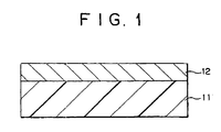
- FIG. 1 is a schematic view illustrating one step of producing a p-type nitride based III-V compound semiconductor according to one embodiment of the present invention.
- a method of producing a p-type nitride based III-V compound semiconductor of the present invention there is produced a p-type nitride based III-V compound semiconductor containing at least one kind selected from group IIIB elements in the short form of the periodic table, which include gallium (Ga), aluminum (Al), indium (In), and boron (B); at least nitrogen selected from group VB elements in the short-form of the periodic table, which include nitrogen (N), arsenic (As), and phosphorus (P); and a p-type impurity.
- the p-type impurity there may be used at least one kind selected from a group consisting of magnesium (Mg), zinc (Zn), carbon (C), beryllium (Be), calcium (Ca), barium (Ba), and cadmium (Cd).
- magnesium is preferably used as the p-type impurity.
- the p-type nitride based III-V compound semiconductor produced by the production method of the present invention is represented by p-type GaN, p-type InN, p-type AlN, p-type AlGaN compound crystal, p-type GaInN compound crystal, or p-type AlInGaN compound crystal.
- a nitride based III-V compound semiconductor 12 containing at least one kind selected from the above-described group IIIB elements, at least nitrogen selected from the above-described group VB elements, and magnesium as a p-type impurity is grown on a c-plane of a substrate 11 made from sapphire ( ⁇ -Al 2 O 3 ) by an MOCVD process or the like.
- Raw materials used for growing the nitride based III-V compound semiconductor 12 by the MOCVD process are as follows: namely, trimethyl gallium ((CH 3 ) 3 Ga) is used as a source gas of gallium; trimethyl aluminum ((CH 3 ) 3 Al) is used as a source gas of aluminum; trimethyl indium ((CH 3 ) 3 In) is used as a source gas of indium; trimethyl boron ((CH 3 ) 3 B) is used as a source gas of boron; ammonia (NH 3 ) is used as a source gas of nitrogen; and bis(cyclopentadienyl) magnesium ((C 5 H 5 ) 2 Mg) is used as a source gas of magnesium.
- the nitride based III-V compound semiconductor 12 thus grown contains hydrogen atoms in a concentration of about 1 ⁇ 10 19 atoms/cm 3 to 1 ⁇ 10 20 atoms/cm 3 .
- the hydrogen atoms which have been produced by decomposition of ammonia as a source gas of nitrogen during the MOCVD process, are liable to be bonded to the p-type impurity.
- FIG. 2 shows a schematic structure of an impurity activation system used for the present invention.
- the impurity activation system includes a chamber 20 having a chamber main body 21.
- the RF electrode 22 is fixed to a supporting base 24, and the RF electrode 23 is supported by a liftable supporting member 25.
- thermocouple 26 On the side opposed to the RF electrode 22, of the RF electrode 23, a thermocouple 26 is provided in a closely contact state, and further a heating mechanism such as a heater 27 is provided.
- the thermocouple 26 and the heater 27 are connected to power sources (not shown), respectively.
- An RF generator 42 is connected to the RF electrode 22 via an impedance matching unit 30 and an amplifier 41.
- the impedance matching unit 30 includes a coil 31 and variable capacitors 32 and 33.
- the RF generator 42 generates a radio frequency in a range of 100 kHz to 400 MHz.
- the radio frequency thus generated is amplified at a specific level by the amplifier 41.
- the radio frequency amplified by the amplifier 41 is monitored by a monitor unit 43.
- a vacuum pump 50 and a pressure device are connected to the chamber 20 for adjusting the inner pressure and atmosphere in the chamber main body 21.
- the substrate 11 on which the nitride based III-V compound semiconductor 12 has been formed is placed between the RF electrodes 22 and 23, and the position of the RF electrode 23 is adjusted by movement of the supporting member 25 in such a manner that the RF electrode 23 is brought into contact with the nitride based III-V compound semiconductor 12.
- an RF voltage is applied between the RF electrodes 22 and 23, to generate an RF field in the chamber 20, thereby applying the RF field to the nitride based III-V compound semiconductor 12.
- hydrogen contained in the nitride based III-V compound semiconductor 12 is released therefrom, with a result that the p-type impurity is activated.
- Such activation of the p-type impurity may be conceived to be based on the following principle.
- an RF field is applied to the nitride based III-V compound semiconductor 12
- electrons present in the nitrogen based III-V compound semiconductor 12 attack the bonding between the p-type impurity and hydrogen, to cut the bonding.
- the hydrogen may be present in the nitride based III-V compound semiconductor 12 in the form of ions (H + ) or radicals (H*).
- the hydrogen floating in the form of ions (H + ) is accelerated by the electric field, and is released as hydrogen molecules (H 2 ) from a gap between the nitrogen based III-V compound semiconductor 12 and the RF electrode 23.
- the hydrogen floating in the form of radicals (H*) collides with hydrogen ions (H + ) or electrons accelerated by the electric field. At this time, the kinetic energy of the hydrogen ions (H + ) or electrons is transmitted to the hydrogen radicals (H*). Accordingly, the diffusion of the hydrogen radicals (H*) is promoted, with a result that the hydrogen in the form of radicals (H*) is released as hydrogen molecules (H 2 ) from the gap between the nitrogen based III-V compound semiconductor 12 and the RF electrode 23.
- the frequency of the RF field is preferably more than 0 Hz and not more than 100 GHz. This is because it is difficult to manufacture an impurity activation system capable of ensuring a radio frequency in a range of more than 100 GHz with a high output, and to realize desirable impedance matching for the radio frequency in the range of more than 100 GHz.
- the frequency of the RF field is preferably in a range of 10 kHz to 400 MHz, more preferably, 1 MHz to 40 MHz.
- the field strength is preferably in a range of 100 V/cm to 1.5 MV/cm. If the field strength is smaller than 100 V/cm, the energy required for accelerating electrons present in the nitride based III-V compound semiconductor 12 becomes small, with a result that the bonding between the p-type impurity and hydrogen cannot be cut, whereas if the field strength is more than 1.5 MV/cm, the nitrogen based III-V compound semiconductor may be broken by the electric field.
- the inner pressure of the chamber main body 21 may be set to be either a reduced pressure, a normal pressure, or an increased pressure, and the atmosphere of the chamber main body 21 may be set to be an inert gas atmosphere such as a nitrogen gas atmosphere or atmospheric air.
- the increased pressure is preferably in a range of 1 ⁇ 10 6 Pa (10 atm) or less. The reason for this is that it is difficult to manufacture an impurity activation system capable of withstanding the inner pressure increased to a value of 1 ⁇ 10 6 Pa (10 atm) or more.
- the reduced pressure atmosphere is preferably set to a vacuum atmosphere of 1 ⁇ 10 -2 Pa or less, particularly, an ultra-high vacuum atmosphere of 1 ⁇ 10 -3 Pa or less in order to prevent the occurrence of discharge and make the release of hydrogen easier.
- An RF field with no bias may be applied to the nitride based III-V compound semiconductor 12; however, an RF field with a bias may be applied to the semiconductor 12 by making the RF electrode 23 on the semiconductor 12 side negative and the RF electrode 22 on the substrate 11 side positive.
- a self-bias may be generated by setting the atmosphere of the inside of the chamber main body 21 to an inert gas atmosphere and shifting the inner pressure from a value of 1 ⁇ 10 -2 Pa or more to atmospheric pressure, thereby generating a plasma, or a bias may be generated by controlling a voltage applied between the RF electrodes 22 and 23 by using a DC power source.
- the nitrogen based III-V compound semiconductor 12 may be heated by the heater 27 or may not be heated.
- the activation of a p-type impurity is not dependent on the heating of the semiconductor 12 so much.
- the heating temperature is preferably set to be less than 400°C. If the heating temperature is equal to or more than 400°C, nitrogen is liable to be released from the nitrogen based III-V compound semiconductor 12, to degrade the crystallinity of the semiconductor 12. It is to be noted that the temperature measured by the thermocouple 26 is little changed even by applying an RF field and is substantially kept at the temperature heated by the heater 27.
- the nitride based III-V compound semiconductor 12 With the above activation of the p-type impurity, the nitride based III-V compound semiconductor 12 becomes a p-type nitride based III-V compound semiconductor.
- FIG. 3 shows a configuration of a semiconductor laser fabricated by using the method of producing a p-type nitride III-V compound semiconductor according to the embodiment of the present invention.
- an organic metal as a raw material of a specific element selected from group IIIB elements, ammonia as a raw material of nitrogen, an organic metal as a raw material of magnesium to be added as a p-type impurity, and monosilane (SiH 4 ) as a raw material of silicon to be added as an n-type impurity are prepared.
- a substrate 61 made from sapphire is disposed in an MOCVD system (not shown), and a buffer layer 62 made from GaN is formed on a c-plane of the substrate 61 by the MOCVD process.
- n-type nitride based III-V compound semiconductor layers are grown on the buffer layer 62 as follows: namely, an n-side contact layer 63 made from n-type GaN doped with silicon, an n-type cladding layer 64 made from n-type AlGaN compound crystal doped with silicon, and an n-type guide layer 65 made from n-type GaN doped with silicon are sequentially grown on the buffer layer 62.
- an active layer 66 having a multiple quantum well structure composed of a stack of compound crystal layers made from Ga x In 1-x N (x differs for each layer in a range of 0 ⁇ x ⁇ 1) is grown on the n-type nitride based III-V compound semiconductor layers.
- respective nitride based III-V compound semiconductor layers each containing a p-type impurity are grown on the active layer 66 as follows: namely, a p-type guide layer 67 made from GaN doped with magnesium, a p-type cladding layer 68 made from AlGaN compound crystal doped with magnesium, and a p-side contact layer 69 made from GaN doped with magnesium are sequentially grown on the active layer 66.
- the p-type impurities contained in the p-type guide layer 67, p-type cladding layer 68, and p-side contact layer 69 are activated by using the same impurity activation system as that shown in FIG. 2 in accordance with the above-described activation manner used for the method of producing a p-type nitride based III-V compound semiconductor, whereby the nitride based III-V compound semiconductor layers are converted into p-type nitride based compound semiconductor layers.
- a resist pattern (not shown) having a stripe shape is formed on the p-type contact layer 69 at a position corresponding to a formation position of an n-side electrode 71 to be described later. Then, the p-type contact layer 69, p-type cladding layer 68, p-type guide layer 67, active layer 66, n-type guide layer 65, and n-type cladding layer 64 are selectively removed in sequence by, for example, RIE (Reactive Ion Etching) using the resist pattern as a mask, to expose the n-side contact layer 63. Subsequently, the resist pattern (not shown) is removed, and the n-side electrode 71 is formed on the n-side contact layer 63 thus exposed. Further, a p-type electrode 72 is formed on the p-side contact layer 69. In this way, a semiconductor layer shown in FIG. 3 is produced.
- RIE Reactive Ion Etching
- the method of producing a p-type nitride based III-V compound semiconductor in this embodiment hydrogen contained in a nitride based III-V compound semiconductor can be simply released by using a simple system, thereby simply activating a p-type impurity. That is the activation of a p-type impurity can be easily carried out without the need of provision of a protective film for preventing the release of nitrogen or provision of electrodes for injecting a current. Accordingly, the production method in this embodiment is proved to be excellent in mass-productivity, and therefore, can be easily put into practical use.
- the nitride based III-V compound semiconductor 12 is not required to be heated by the heating mechanism such as the heater 27, or if the semiconductor 12 is required to be heated, the heating effect can be sufficiently achieved by heating the semiconductor 12 at a temperature less than 400°C, and accordingly, it is possible to eliminate or shorten the heating time and cooling time and hence to enhance the production efficiency, and further, it is possible to eliminate the need of provision of any member having a high heat resistance and hence to simplify the production apparatus. Further, since the semiconductor 12 is not required to be kept at a high temperature for a long time, it is possible to prevent the release of nitrogen, and hence to produce a p-type nitride based III-V compound semiconductor having a high crystallinity and a low resistance. Accordingly, a semiconductor device (semiconductor laser in this embodiment) produced by the production method is advantageous in improving device characteristics, more specifically, enhancing the light emission efficiency of the device and prolonging the service life thereof.
- Each of the samples in Inventive Examples 1 to 16 was produced, as shown in Fig. 4, by sequentially growing, on a c-plane of a substrate 81 made from sapphire, a buffer layer 82 made from undoped GaN having a thickness of 40 nm, an underlying layer 83 made from undoped GaN having a thickness of 1.0 ⁇ m, and a nitrogen based III-V compound semiconductor layer 84 doped with magnesium as a p-type impurity and having a thickness of 1.0 ⁇ m; and applying an RF field to the nitrogen based III-V compound semiconductor layer 84 under the following condition by using the same impurity activation system as that shown in FIG. 2, to activate the p-type impurity, thereby converting the nitride based III-V compound semiconductor layer 84 into a p-type nitride based III-V compound semiconductor layer.
- the activation conditions for the samples were as follow: namely, the voltage, field strength, and application time were changed, as shown in Table 1, for the samples in Inventive example 1 to 16; the frequency of the RF field was set to 13.56 MHz and the atmosphere of the inside of the chamber 20 was set to an ultra-high vacuum of 1 ⁇ 10 -3 Pa or less for the samples in Inventive Examples 1 to 16; and the nitrogen based III-V compound semiconductor 84 was heated to 300°C by the heater 27 for the samples in Inventive examples 1 to 12, and the heating by the heater 27 was not performed for the samples in Inventive Examples 13 to 16. The heating temperature was measured by the thermocouple 26. The measured value by the thermocouple 26 was little changed even by applying an RF field.
- Each of the samples in Inventive Examples 1 to 16 was measured in terms of Hall effect by cutting the sample into a size of 5 mm ⁇ 5 mm, and forming electrodes at four comers of the surface of the p-type nitride based III-V compound semiconductor layer of the sample.
- the electrode used for the measurement was formed by stacking a nickel (Ni) layer, a platinum layer, and a gold layer in this order from the side of the p-type nitride based III-V compound semiconductor layer.
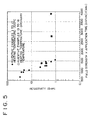
- Resistivity, mobility, and carrier density of each sample obtained by measurement of the Hall effect were shown in Table 2. Further, a relationship between the resistivity and the field strength ⁇ application time (product of the field strength and the application time) is shown in FIG.
- a sample in the Comparative Example was produced in the same manner as described in Inventive Example 1 except that an electrostatic field having a field strength of 70 kV/cm was applied for 10 min in place of an RF field.
- the sample in the Comparative Example was measured in terms of Hall effect in the same manner as that described in Inventive Example 1. As a result, the activation of a p-type impurity in the sample in Comparative Example could not be recognized.
- the results of Inventive Examples 1 to 16 and Comparative Example show that the p-type impurity can be easily activated by applying an RF field.
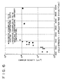
- the data in FIGS. 5 and 6 show that the resistivity is reduced with an increase in the product of a field strength and an application time and the carrier density is increased with an increase in the product of a field strength and an application time, and that each of the resistivity and the carrier density becomes substantially constant when the product of a field strength and an application time exceeds 1500 (kV/cm) ⁇ (sec).
- each of the resistivity and carrier density is not dependent on the heating of the nitrogen based III-V compound semiconductor 84 by the heater 27. That is to say, it is revealed that the p-type impurity can be activated without heating the nitride based III-V compound semiconductor 84 by the heating mechanism such as the heater 27.
- the RF electrode 23 is brought into contact with the nitride based III-V compound semiconductor 12; however, the RF electrode 23 may be disposed in such a manner as to be spaced from the nitride based III-V compound semiconductor 12.
- hydrogen is allowed to be released from a gap between the nitrogen based III-V compound semiconductor 12 and the RF electrode 23; however, if the surface of the nitrogen based III-V compound semiconductor 12 is flattened and the RF electrode 23 can be brought into tight-contact with the flattened surface of the semiconductor 12, the RF electrode 23 may be made from a hydrogen absorbable or permeable material, or a hydrogen release assisting member made from a hydrogen absorbable or permeable material may be provided on a surface, on the semiconductor 12 side, of the RF electrode 23. With this configuration, even in the case where a gap between the nitrogen based III-V compound semiconductor 12 and the RF electrode 23 is narrow, it is possible to prevent the release of hydrogen from being blocked.
- hydrogen absorbable or permeable materials may include an alloy of nickel (Ni) and lanthanum (La) or magnesium (Mg), an alloy of titanium (Ti) and manganese (Mn), iron (Fe), and cobalt (Co) or vanadium (V), an alloy of zinc (Zn) and manganese, an alloy of vanadium, titanium, and chromium (Cr), and palladium (Pd).
- the nitride based III-V compound semiconductor 12 is produced by the MOCVD process; however, the semiconductor 12 may be produced by an MBE (Molecular Beam Epitaxy) process, a hydride vapor-phase growth process, or halide vapor-phase growth process.
- MBE Molecular Beam Epitaxy
- the hydride vapor-phase process is characterized in that a hydride contributes to the reaction and transfer of a source gas
- the halide vapor-phase growth process is characterized in that a halide contributes to the reaction and transfer of a source gas.
- the substrates 11 and 61 made from sapphire are used; however, the substrate may be made from a material other than sapphire, such as GaN or SiC.
- the method of fabricating a semiconductor device has been described by example of a semiconductor laser as the semiconductor device; however, the present invention can be applied to a method of fabricating another semiconductor device using a p-type nitride based III-V compound semiconductor, such as a light emitting diode or a hetero-junction bipolar transistor (HBT).
- a p-type nitride based III-V compound semiconductor such as a light emitting diode or a hetero-junction bipolar transistor (HBT).
Landscapes
- Chemical & Material Sciences (AREA)
- Engineering & Computer Science (AREA)
- Crystallography & Structural Chemistry (AREA)
- Materials Engineering (AREA)
- Metallurgy (AREA)
- Organic Chemistry (AREA)
- Inorganic Chemistry (AREA)
- Led Devices (AREA)
- Semiconductor Lasers (AREA)
- Crystals, And After-Treatments Of Crystals (AREA)
Abstract
Description

| Resistivity (Ωcm) | Mobility (cm2/Vs) | Carrier density (cm-3) | |
| Inventive Example 1 | 4.27 | 7.28 | 2.01×10¹⁷ |
| Inventive Example 2 | 30.2 | 7.06 | 2.93 ×10¹⁶ |
| Inventive Example 3 | 31.4 | 3.45 | 5.76×10¹⁶ |
| Inventive Example 4 | 22.4 | 6.55 | 4.25×10¹⁶ |
| Inventive Example 5 | 27 | 4.51 | 5.12×10¹⁶ |
| Inventive Example 6 | 12.9 | 7.17 | 6.77×10¹⁶ |
| Inventive Example 7 | 21 | 5.37 | 5.53 ×10¹⁶ |
| Inventive Example 8 | 2.33 | 5.45 | 4.92×10¹⁷ |
| Inventive Example 9 | 2.68 | 6.39 | 3.65×10¹⁷ |
| Inventive Example 10 | 1.5 | 4.63 | 9.01×10¹⁷ |
| Inventive Example 11 | 2.47 | 5.13 | 4.92×10¹⁷ |
| Inventive Example 12 | 1.04 | 4.7 | 1.27×10¹⁸ |
| Inventive Example 13 | 2.41 | 7.39 | 3.51×10¹⁷ |
| Inventive Example 14 | 3.79 | 7.71 | 2.14×10¹⁷ |
| Inventive Example 15 | 1.42 | 6.45 | 6.80×10¹⁷ |
| Inventive Example 16 | 1.47 | 5.12 | 8.31×10¹⁷ |
Claims (6)
- A method of producing a p-type nitride based III-V compound semiconductor, comprising the steps of:preparing a nitride based III-V compound semiconductor (12) containing at least one kind selected from group IIIB elements, at least nitrogen selected from group VB elements, and a p-type impurity; andapplying a radio frequency field to said nitride based III-V compound semiconductor (12).
- A method of producing a p-type nitride based III-V compound semiconductor according to claim 1, wherein hydrogen (H) is released from said nitride based III-V compound semiconductor (12) by applying a radio frequency field to said compound semiconductor (12).
- A method of producing a p-type nitride based III-V compound semiconductor according to claim 1, wherein a frequency of the radio frequency field to be applied to said compound semiconductor (12) is in a range of 100 GHz or less.
- A method of producing a p-type nitride based III-V compound semiconductor according to claim 1, wherein a field strength of the radio frequency field to be applied to said compound semiconductor (12) is in a range of 100 V/cm to 1.5 MV/cm.
- A method of producing a p-type nitride based III-V compound semiconductor according to claim 1, wherein the radio frequency field is applied to said compound semiconductor (12) under a reduced pressure, a normal pressure, or an increased pressure of 1 × 10⁶ Pa or less.
- A method of fabricating a semiconductor device, comprising the step of:
producing a p-type nitride based III-V compound semiconductor by preparing a nitride based III-V compound semiconductor (12) containing at least one kind selected from group IIIB elements, at least nitrogen selected from group VB elements, and a p-type impurity and applying a radio frequency field to said nitride based III-V compound semiconductor (12) thus prepared.
Applications Claiming Priority (4)
| Application Number | Priority Date | Filing Date | Title |
|---|---|---|---|
| JP2000102622 | 2000-04-04 | ||
| JP2000102622 | 2000-04-04 | ||
| JP2000247844A JP4618465B2 (en) | 2000-04-04 | 2000-08-17 | P-type nitride III-V compound semiconductor manufacturing method and semiconductor device manufacturing method |
| JP2000247844 | 2000-08-17 |
Publications (3)
| Publication Number | Publication Date |
|---|---|
| EP1143503A2 true EP1143503A2 (en) | 2001-10-10 |
| EP1143503A3 EP1143503A3 (en) | 2005-08-31 |
| EP1143503B1 EP1143503B1 (en) | 2013-08-07 |
Family
ID=26589458
Family Applications (1)
| Application Number | Title | Priority Date | Filing Date |
|---|---|---|---|
| EP01400872.6A Expired - Lifetime EP1143503B1 (en) | 2000-04-04 | 2001-04-04 | Method of producing P-type nitride based III-V compound semiconductor and method of fabricating semiconductor device using the same |
Country Status (5)
| Country | Link |
|---|---|
| US (1) | US6524882B2 (en) |
| EP (1) | EP1143503B1 (en) |
| JP (1) | JP4618465B2 (en) |
| KR (1) | KR100747062B1 (en) |
| TW (1) | TW492113B (en) |
Families Citing this family (17)
| Publication number | Priority date | Publication date | Assignee | Title |
|---|---|---|---|---|
| US6525413B1 (en) * | 2000-07-12 | 2003-02-25 | Micron Technology, Inc. | Die to die connection method and assemblies and packages including dice so connected |
| US6727167B2 (en) * | 2000-10-13 | 2004-04-27 | Emcore Corporation | Method of making an aligned electrode on a semiconductor structure |
| GB2376563A (en) * | 2001-06-13 | 2002-12-18 | Sharp Kk | A method of growing a magnesium-doped nitride semiconductor material |
| JP3866540B2 (en) * | 2001-07-06 | 2007-01-10 | 株式会社東芝 | Nitride semiconductor device and manufacturing method thereof |
| US6720570B2 (en) * | 2002-04-17 | 2004-04-13 | Tekcore Co., Ltd. | Gallium nitride-based semiconductor light emitting device |
| EP1783824A4 (en) * | 2004-08-06 | 2009-04-01 | Sumitomo Electric Industries | METHOD FOR MANUFACTURING P-TYPE SEMICONDUCTORS AND SEMICONDUCTOR ELEMENT |
| WO2006112167A1 (en) | 2005-04-01 | 2006-10-26 | Sharp Kabushiki Kaisha | METHOD FOR MANUFACTURING p TYPE NITRIDE SEMICONDUCTOR AND SEMICONDUCTOR DEVICE MANUFACTURED BY SUCH METHOD |
| JP4980594B2 (en) * | 2005-08-03 | 2012-07-18 | 京セラ株式会社 | Method for producing P-type gallium nitride compound semiconductor |
| JP4742791B2 (en) * | 2005-09-30 | 2011-08-10 | 豊田合成株式会社 | Method for p-type activation of group III nitride compound semiconductor |
| KR100708934B1 (en) * | 2005-11-15 | 2007-04-17 | 삼성전기주식회사 | Nitride semiconductor light emitting device |
| JP2007311375A (en) * | 2006-05-16 | 2007-11-29 | Showa Denko Kk | A manufacturing method of a p-type III-V compound semiconductor and a manufacturing method of a light emitting element. |
| EP2201613A1 (en) * | 2007-08-31 | 2010-06-30 | Lattice Power (Jiangxi) Corporation | Method for fabricating a low-resistivity ohmic contact to a p-type iii-v nitride semiconductor material at low temperature |
| CN101918624A (en) * | 2008-01-16 | 2010-12-15 | 国立大学法人东京农工大学 | Method for producing a laminate having an A1-based group III nitride single crystal layer, a laminate obtained by the production method, a method for producing an A1-based group III nitride single-crystal substrate using the laminate, and an aluminum nitride single-crystal substrate |
| JP5545272B2 (en) * | 2011-06-21 | 2014-07-09 | 豊田合成株式会社 | Group III nitride semiconductor light emitting device |
| JP5699983B2 (en) * | 2012-04-27 | 2015-04-15 | 住友電気工業株式会社 | Method for fabricating gallium nitride based semiconductor, method for fabricating group III nitride semiconductor device, and group III nitride semiconductor device |
| TWI730472B (en) * | 2019-10-25 | 2021-06-11 | 進化光學有限公司 | Full color led display panel using isolation lines of laser scribing and manufacturing method thereof |
| CN118156122B (en) * | 2024-05-11 | 2024-08-20 | 苏州立琻半导体有限公司 | Electrochemical processing equipment for nitride semiconductor and processing technology for wafer doping |
Family Cites Families (20)
| Publication number | Priority date | Publication date | Assignee | Title |
|---|---|---|---|---|
| JP2540791B2 (en) | 1991-11-08 | 1996-10-09 | 日亜化学工業株式会社 | A method for manufacturing a p-type gallium nitride-based compound semiconductor. |
| JP3672585B2 (en) * | 1994-03-22 | 2005-07-20 | 豊田合成株式会社 | Method for manufacturing group 3 nitride semiconductor |
| US6218677B1 (en) * | 1994-08-15 | 2001-04-17 | Texas Instruments Incorporated | III-V nitride resonant tunneling |
| JPH0888432A (en) | 1994-09-16 | 1996-04-02 | Rohm Co Ltd | Production of semiconductor laser |
| JP3461074B2 (en) | 1995-12-12 | 2003-10-27 | パイオニア株式会社 | Method of manufacturing group III nitride semiconductor light emitting device |
| JPH102001A (en) * | 1996-06-15 | 1998-01-06 | Okajima Kogyo Kk | Grating |
| JPH101999A (en) * | 1996-06-17 | 1998-01-06 | Kyowa Plast Sangyo Kk | Coupling flange for toilet stool and connecting structure of the flange and toilet stool |
| JP3688843B2 (en) * | 1996-09-06 | 2005-08-31 | 株式会社東芝 | Nitride semiconductor device manufacturing method |
| JP3381534B2 (en) * | 1996-11-19 | 2003-03-04 | ソニー株式会社 | Self-oscillation type semiconductor laser |
| JPH10242578A (en) | 1997-02-26 | 1998-09-11 | Matsushita Electric Ind Co Ltd | Manufacturing method of gallium nitride based semiconductor light emitting device |
| TW329058B (en) * | 1997-03-20 | 1998-04-01 | Ind Tech Res Inst | Manufacturing method for P type gallium nitride |
| JPH10335637A (en) * | 1997-05-30 | 1998-12-18 | Sony Corp | Heterojunction field effect transistor |
| JP3433075B2 (en) * | 1997-11-19 | 2003-08-04 | 株式会社東芝 | Method of manufacturing nitride semiconductor device |
| JP3697106B2 (en) * | 1998-05-15 | 2005-09-21 | キヤノン株式会社 | Method for manufacturing semiconductor substrate and method for manufacturing semiconductor thin film |
| JP2000058919A (en) * | 1998-08-13 | 2000-02-25 | Toshiba Corp | Semiconductor device and manufacturing method thereof |
| JP3794876B2 (en) * | 1998-09-09 | 2006-07-12 | 松下電器産業株式会社 | Manufacturing method of semiconductor device |
| JP3723374B2 (en) * | 1999-03-19 | 2005-12-07 | ローム株式会社 | Manufacturing method of semiconductor light emitting device |
| US6475277B1 (en) * | 1999-06-30 | 2002-11-05 | Sumitomo Electric Industries, Ltd. | Group III-V nitride semiconductor growth method and vapor phase growth apparatus |
| JP2001044209A (en) * | 1999-07-27 | 2001-02-16 | Furukawa Electric Co Ltd:The | Manufacturing method of GaN-based semiconductor device |
| TW449931B (en) * | 2000-01-27 | 2001-08-11 | United Epitaxy Co Ltd | Manufacturing method of P-type semiconductor with a low resistance coefficient |
-
2000
- 2000-08-17 JP JP2000247844A patent/JP4618465B2/en not_active Expired - Fee Related
-
2001
- 2001-04-03 KR KR1020010017632A patent/KR100747062B1/en not_active Expired - Fee Related
- 2001-04-03 US US09/824,238 patent/US6524882B2/en not_active Expired - Fee Related
- 2001-04-03 TW TW090108004A patent/TW492113B/en not_active IP Right Cessation
- 2001-04-04 EP EP01400872.6A patent/EP1143503B1/en not_active Expired - Lifetime
Also Published As
| Publication number | Publication date |
|---|---|
| JP4618465B2 (en) | 2011-01-26 |
| TW492113B (en) | 2002-06-21 |
| KR100747062B1 (en) | 2007-08-07 |
| US6524882B2 (en) | 2003-02-25 |
| KR20010095267A (en) | 2001-11-03 |
| EP1143503A3 (en) | 2005-08-31 |
| EP1143503B1 (en) | 2013-08-07 |
| JP2001351925A (en) | 2001-12-21 |
| US20010055871A1 (en) | 2001-12-27 |
Similar Documents
| Publication | Publication Date | Title |
|---|---|---|
| EP1143503B1 (en) | Method of producing P-type nitride based III-V compound semiconductor and method of fabricating semiconductor device using the same | |
| EP0881666B2 (en) | P-type nitrogen compound semiconductor and method of manufacturing same | |
| US7176479B2 (en) | Nitride compound semiconductor element | |
| US5929466A (en) | Semiconductor device and method of fabricating the same | |
| JP3688843B2 (en) | Nitride semiconductor device manufacturing method | |
| JP3754120B2 (en) | Semiconductor light emitting device | |
| US7714350B2 (en) | Gallium nitride based semiconductor device and method of manufacturing same | |
| JPH05183189A (en) | Manufacture of p-type gallium nitride based compound semiconductor | |
| US20080308836A1 (en) | Nitride Semiconductor Device and Method for Growing Nitride Semiconductor Crystal Layer | |
| JP2000216164A (en) | Method for manufacturing semiconductor device | |
| US7537944B2 (en) | Method for manufacturing p-type group III nitride semiconductor, and group III nitride semiconductor light-emitting device | |
| JP3254931B2 (en) | Method for producing p-type gallium nitride-based compound semiconductor | |
| EP1037268A1 (en) | METHOD FOR SYNTHESIZING SINGLE CRYSTAL AlN THIN FILMS OF LOW RESISTANT n-TYPE AND LOW RESISTANT p-TYPE | |
| JP4444230B2 (en) | Gallium nitride semiconductor device | |
| JP2003178987A (en) | Method for manufacturing nitride-based compound semiconductor, nitride-based compound semiconductor wafer, and nitride-based compound semiconductor device | |
| JP2002151415A (en) | Nitride-based semiconductor device, nitride-based semiconductor substrate, and methods for manufacturing the same | |
| JP3180710B2 (en) | Method of manufacturing gallium nitride based compound semiconductor light emitting device | |
| JP3301345B2 (en) | Method for forming p-type gallium nitride-based compound semiconductor layer | |
| JPH10178213A (en) | Gallium nitride based compound semiconductor light emitting device | |
| JPH11135831A (en) | Gallium nitride based compound semiconductor wafer and compound semiconductor device | |
| JPH10178208A (en) | Method of converting gallium nitride-based compound semiconductor to p-type | |
| JPH10178205A (en) | Method of converting gallium nitride-based compound semiconductor to p-type | |
| JPH10178209A (en) | Gallium nitride based compound semiconductor | |
| JP2002305325A (en) | Method of manufacturing gallium nitride based compound semiconductor light emitting device | |
| JPH11330550A (en) | Group iii-v compound semiconductor element, and its manufacture |
Legal Events
| Date | Code | Title | Description |
|---|---|---|---|
| PUAI | Public reference made under article 153(3) epc to a published international application that has entered the european phase |
Free format text: ORIGINAL CODE: 0009012 |
|
| AK | Designated contracting states |
Kind code of ref document: A2 Designated state(s): AT BE CH CY DE DK ES FI FR GB GR IE IT LI LU MC NL PT SE TR |
|
| AX | Request for extension of the european patent |
Free format text: AL;LT;LV;MK;RO;SI |
|
| PUAL | Search report despatched |
Free format text: ORIGINAL CODE: 0009013 |
|
| AK | Designated contracting states |
Kind code of ref document: A3 Designated state(s): AT BE CH CY DE DK ES FI FR GB GR IE IT LI LU MC NL PT SE TR |
|
| AX | Request for extension of the european patent |
Extension state: AL LT LV MK RO SI |
|
| RIC1 | Information provided on ipc code assigned before grant |
Ipc: 7H 01L 21/322 B Ipc: 7C 30B 33/00 A |
|
| 17P | Request for examination filed |
Effective date: 20060209 |
|
| AKX | Designation fees paid |
Designated state(s): DE FR GB |
|
| REG | Reference to a national code |
Ref country code: DE Ref legal event code: R079 Ref document number: 60148217 Country of ref document: DE Free format text: PREVIOUS MAIN CLASS: C30B0033000000 Ipc: H01L0021322000 |
|
| GRAP | Despatch of communication of intention to grant a patent |
Free format text: ORIGINAL CODE: EPIDOSNIGR1 |
|
| RIC1 | Information provided on ipc code assigned before grant |
Ipc: H01L 21/322 20060101AFI20130201BHEP Ipc: C30B 29/40 20060101ALI20130201BHEP |
|
| GRAS | Grant fee paid |
Free format text: ORIGINAL CODE: EPIDOSNIGR3 |
|
| GRAA | (expected) grant |
Free format text: ORIGINAL CODE: 0009210 |
|
| AK | Designated contracting states |
Kind code of ref document: B1 Designated state(s): DE FR GB |
|
| REG | Reference to a national code |
Ref country code: GB Ref legal event code: FG4D |
|
| REG | Reference to a national code |
Ref country code: DE Ref legal event code: R096 Ref document number: 60148217 Country of ref document: DE Effective date: 20130926 |
|
| PLBE | No opposition filed within time limit |
Free format text: ORIGINAL CODE: 0009261 |
|
| STAA | Information on the status of an ep patent application or granted ep patent |
Free format text: STATUS: NO OPPOSITION FILED WITHIN TIME LIMIT |
|
| 26N | No opposition filed |
Effective date: 20140508 |
|
| REG | Reference to a national code |
Ref country code: DE Ref legal event code: R097 Ref document number: 60148217 Country of ref document: DE Effective date: 20140508 |
|
| PGFP | Annual fee paid to national office [announced via postgrant information from national office to epo] |
Ref country code: DE Payment date: 20140418 Year of fee payment: 14 |
|
| GBPC | Gb: european patent ceased through non-payment of renewal fee |
Effective date: 20140404 |
|
| REG | Reference to a national code |
Ref country code: FR Ref legal event code: ST Effective date: 20141231 |
|
| PG25 | Lapsed in a contracting state [announced via postgrant information from national office to epo] |
Ref country code: GB Free format text: LAPSE BECAUSE OF NON-PAYMENT OF DUE FEES Effective date: 20140404 |
|
| PG25 | Lapsed in a contracting state [announced via postgrant information from national office to epo] |
Ref country code: FR Free format text: LAPSE BECAUSE OF NON-PAYMENT OF DUE FEES Effective date: 20140430 |
|
| REG | Reference to a national code |
Ref country code: DE Ref legal event code: R119 Ref document number: 60148217 Country of ref document: DE |
|
| PG25 | Lapsed in a contracting state [announced via postgrant information from national office to epo] |
Ref country code: DE Free format text: LAPSE BECAUSE OF NON-PAYMENT OF DUE FEES Effective date: 20151103 |