EP1139433B1 - Semiconductor device having a Schottky barrier diode structure - Google Patents
Semiconductor device having a Schottky barrier diode structure Download PDFInfo
- Publication number
- EP1139433B1 EP1139433B1 EP01108152A EP01108152A EP1139433B1 EP 1139433 B1 EP1139433 B1 EP 1139433B1 EP 01108152 A EP01108152 A EP 01108152A EP 01108152 A EP01108152 A EP 01108152A EP 1139433 B1 EP1139433 B1 EP 1139433B1
- Authority
- EP
- European Patent Office
- Prior art keywords
- semiconductor
- layer
- filled material
- semiconductor layer
- impurity concentration
- Prior art date
- Legal status (The legal status is an assumption and is not a legal conclusion. Google has not performed a legal analysis and makes no representation as to the accuracy of the status listed.)
- Expired - Lifetime
Links
- 239000004065 semiconductor Substances 0.000 title claims description 134
- 230000004888 barrier function Effects 0.000 title description 9
- 239000000463 material Substances 0.000 claims description 68
- 239000012535 impurity Substances 0.000 claims description 34
- 230000015556 catabolic process Effects 0.000 claims description 28
- 229910052751 metal Inorganic materials 0.000 claims description 7
- 239000002184 metal Substances 0.000 claims description 7
- 230000005684 electric field Effects 0.000 description 20
- 239000000758 substrate Substances 0.000 description 13
- 229910021420 polycrystalline silicon Inorganic materials 0.000 description 8
- 230000006866 deterioration Effects 0.000 description 5
- VYPSYNLAJGMNEJ-UHFFFAOYSA-N Silicium dioxide Chemical compound O=[Si]=O VYPSYNLAJGMNEJ-UHFFFAOYSA-N 0.000 description 4
- 229910052814 silicon oxide Inorganic materials 0.000 description 4
- XUIMIQQOPSSXEZ-UHFFFAOYSA-N Silicon Chemical compound [Si] XUIMIQQOPSSXEZ-UHFFFAOYSA-N 0.000 description 2
- 230000000694 effects Effects 0.000 description 2
- 238000010030 laminating Methods 0.000 description 2
- 238000004519 manufacturing process Methods 0.000 description 2
- 238000000034 method Methods 0.000 description 2
- 229910021421 monocrystalline silicon Inorganic materials 0.000 description 2
- 229910052710 silicon Inorganic materials 0.000 description 2
- 239000010703 silicon Substances 0.000 description 2
- ZOXJGFHDIHLPTG-UHFFFAOYSA-N Boron Chemical compound [B] ZOXJGFHDIHLPTG-UHFFFAOYSA-N 0.000 description 1
- 229910001218 Gallium arsenide Inorganic materials 0.000 description 1
- OAICVXFJPJFONN-UHFFFAOYSA-N Phosphorus Chemical compound [P] OAICVXFJPJFONN-UHFFFAOYSA-N 0.000 description 1
- 229910052785 arsenic Inorganic materials 0.000 description 1
- RQNWIZPPADIBDY-UHFFFAOYSA-N arsenic atom Chemical compound [As] RQNWIZPPADIBDY-UHFFFAOYSA-N 0.000 description 1
- 230000015572 biosynthetic process Effects 0.000 description 1
- 229910052796 boron Inorganic materials 0.000 description 1
- 238000009792 diffusion process Methods 0.000 description 1
- 238000005530 etching Methods 0.000 description 1
- 230000003647 oxidation Effects 0.000 description 1
- 238000007254 oxidation reaction Methods 0.000 description 1
- 230000002093 peripheral effect Effects 0.000 description 1
- 229910052698 phosphorus Inorganic materials 0.000 description 1
- 239000011574 phosphorus Substances 0.000 description 1
- 238000000206 photolithography Methods 0.000 description 1
Images


Classifications
-
- H—ELECTRICITY
- H01—ELECTRIC ELEMENTS
- H01L—SEMICONDUCTOR DEVICES NOT COVERED BY CLASS H10
- H01L29/00—Semiconductor devices adapted for rectifying, amplifying, oscillating or switching, or capacitors or resistors with at least one potential-jump barrier or surface barrier, e.g. PN junction depletion layer or carrier concentration layer; Details of semiconductor bodies or of electrodes thereof ; Multistep manufacturing processes therefor
- H01L29/66—Types of semiconductor device ; Multistep manufacturing processes therefor
- H01L29/66007—Multistep manufacturing processes
- H01L29/66075—Multistep manufacturing processes of devices having semiconductor bodies comprising group 14 or group 13/15 materials
- H01L29/66083—Multistep manufacturing processes of devices having semiconductor bodies comprising group 14 or group 13/15 materials the devices being controllable only by variation of the electric current supplied or the electric potential applied, to one or more of the electrodes carrying the current to be rectified, amplified, oscillated or switched, e.g. two-terminal devices
- H01L29/6609—Diodes
- H01L29/66143—Schottky diodes
-
- H—ELECTRICITY
- H01—ELECTRIC ELEMENTS
- H01L—SEMICONDUCTOR DEVICES NOT COVERED BY CLASS H10
- H01L29/00—Semiconductor devices adapted for rectifying, amplifying, oscillating or switching, or capacitors or resistors with at least one potential-jump barrier or surface barrier, e.g. PN junction depletion layer or carrier concentration layer; Details of semiconductor bodies or of electrodes thereof ; Multistep manufacturing processes therefor
- H01L29/02—Semiconductor bodies ; Multistep manufacturing processes therefor
- H01L29/06—Semiconductor bodies ; Multistep manufacturing processes therefor characterised by their shape; characterised by the shapes, relative sizes, or dispositions of the semiconductor regions ; characterised by the concentration or distribution of impurities within semiconductor regions
- H01L29/0603—Semiconductor bodies ; Multistep manufacturing processes therefor characterised by their shape; characterised by the shapes, relative sizes, or dispositions of the semiconductor regions ; characterised by the concentration or distribution of impurities within semiconductor regions characterised by particular constructional design considerations, e.g. for preventing surface leakage, for controlling electric field concentration or for internal isolations regions
- H01L29/0607—Semiconductor bodies ; Multistep manufacturing processes therefor characterised by their shape; characterised by the shapes, relative sizes, or dispositions of the semiconductor regions ; characterised by the concentration or distribution of impurities within semiconductor regions characterised by particular constructional design considerations, e.g. for preventing surface leakage, for controlling electric field concentration or for internal isolations regions for preventing surface leakage or controlling electric field concentration
- H01L29/0611—Semiconductor bodies ; Multistep manufacturing processes therefor characterised by their shape; characterised by the shapes, relative sizes, or dispositions of the semiconductor regions ; characterised by the concentration or distribution of impurities within semiconductor regions characterised by particular constructional design considerations, e.g. for preventing surface leakage, for controlling electric field concentration or for internal isolations regions for preventing surface leakage or controlling electric field concentration for increasing or controlling the breakdown voltage of reverse biased devices
- H01L29/0615—Semiconductor bodies ; Multistep manufacturing processes therefor characterised by their shape; characterised by the shapes, relative sizes, or dispositions of the semiconductor regions ; characterised by the concentration or distribution of impurities within semiconductor regions characterised by particular constructional design considerations, e.g. for preventing surface leakage, for controlling electric field concentration or for internal isolations regions for preventing surface leakage or controlling electric field concentration for increasing or controlling the breakdown voltage of reverse biased devices by the doping profile or the shape or the arrangement of the PN junction, or with supplementary regions, e.g. junction termination extension [JTE]
- H01L29/063—Reduced surface field [RESURF] pn-junction structures
- H01L29/0634—Multiple reduced surface field (multi-RESURF) structures, e.g. double RESURF, charge compensation, cool, superjunction (SJ), 3D-RESURF, composite buffer (CB) structures
-
- H—ELECTRICITY
- H01—ELECTRIC ELEMENTS
- H01L—SEMICONDUCTOR DEVICES NOT COVERED BY CLASS H10
- H01L29/00—Semiconductor devices adapted for rectifying, amplifying, oscillating or switching, or capacitors or resistors with at least one potential-jump barrier or surface barrier, e.g. PN junction depletion layer or carrier concentration layer; Details of semiconductor bodies or of electrodes thereof ; Multistep manufacturing processes therefor
- H01L29/66—Types of semiconductor device ; Multistep manufacturing processes therefor
- H01L29/86—Types of semiconductor device ; Multistep manufacturing processes therefor controllable only by variation of the electric current supplied, or only the electric potential applied, to one or more of the electrodes carrying the current to be rectified, amplified, oscillated or switched
- H01L29/861—Diodes
- H01L29/872—Schottky diodes
Definitions
- the present invention relates to a semiconductor device, in particular, to a semiconductor device having a Schottky barrier diode structure.
- a Schottky barrier diode While a Schottky barrier diode (SBD) has a low forward voltage and a high switching speed, the SBD has high reverse leakage current and a low reverse avalanche breakdown voltage as its disadvantage. In a medium or high voltage product of 100 V or higher, in particular, the reverse leakage current needs to be reduced to prevent thermorunaway. The impurity concentration of a drift region needs to be lowered so that a depletion layer is expanded while maintaining a high Schottky barrier height. As a result, forward characteristics are deteriorated.
- Fig. 10 shows a structure for reducing leakage current by utilizing a pinch-off effect due to a junction used in a low voltage product.
- an n-type semiconductor layer 2 (hereinafter, referred to as N - epi-layer 2) having a low impurity concentration is formed on an n-type semiconductor substrate 1 (hereinafter, referred to as n-type substrate 1) having a high impurity concentration by epitaxial growth.
- P-type semiconductor regions 19 (hereinafter, referred to as P + regions 19) having a high impurity concentration are disposed at prescribed intervals in the main surface of the N - epi-layer 2 by diffusion or embedding of polycrystalline silicon in the trench.
- An anode electrode film 8 contacted to the main surface 6 of the N - epi-layer 2 and surfaces 20 of the P + regions 19 is formed.
- the anode electrode film 8 has Schottky contact with the main surface 6 of the N - epi-layer 2.
- a cathode electrode film 9 having ohmic contact with the n-type substrate 1 is formed on the other surface of the n-type substrate 1.
- depletion layers 23 1 extend from side surfaces 21, 22 of the P + regions 19 into a region 2a in the N - epi-layer 2 interposed between the adjacent P + regions 19 as shown in Fig. 11 .
- edges of the depletion layers extending from the side surfaces 21, 22 of the P + regions 19 come into contact with each other (pinch-off) and become one wide depletion layer 23 2 . Therefore, an electric field applied to an interface between the main surface 6 of the N - epi-layer 2 and the anode electrode film 8 is relaxed and thereby reverse leakage current can be reduced.
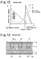
- Fig. 12 shows a distribution of electric field strengths in a vertical direction along lines A and B, which are located at the centers of the P + region 19 and the N - epi-region 2a interposed between the P + regions 19, respectively, when a reverse avalanche breakdown voltage is applied to the semiconductor device in a pinch-off state in Fig. 10 .
- a reverse avalanche breakdown voltage is applied to the semiconductor device in a pinch-off state in Fig. 10 .
- an electric field applied to the interface between the main surface 6 of the N - epi-layer 2 and the anode electrode film 8 is relaxed.
- an object of the present invention is to provide a semiconductor device comprising a Schottky barrier diode in which reverse leakage current is maintained at a conventional level while forward characteristics are greatly improved.
- the present invention provides a semiconductor device having a first semiconductor layer composed of a semiconductor of a first conductivity type, a second semiconductor layer of the first conductivity type having a lower impurity concentration than that of the first semiconductor layer, trench portions composed of thin trenches having a prescribed width and prescribed intervals therebetween formed in the second semiconductor layer surface, a semiconductor filled material composed of semiconductor of a second conductivity type, which is opposite to the first conductivity type, filled in the trench portions, a Schottky metal electrode formed on the surface of the second semiconductor layer and the surface of the semiconductor filled material while forming a Schottky junction with the second semiconductor layer and an ohmic contact with the semiconductor filled material, and an ohmic metal electrode formed on the surface of the first semiconductor layer.
- the second semiconductor layer and the semiconductor filled material are constituted by the same semiconductor material.
- BV AK 60 x E g / 1.1 1.5 x N d / 10 16 - 3 / 4
- N d represents an impurity concentration of the second semiconductor layer and its unit is cm -3
- E g represents an energy band gap value of the semiconductor material and its unit is eV
- the width W m between the semiconductor filled materials adjacent to each other formed in the second semiconductor layers satisfies the following equations (1) and (2): (where the unit of the width W m is cm; W t represents a width W m ⁇ W t ⁇ N ⁇ N ⁇ of the semiconductor filled material and its unit is cm; and N a represents an impurity concentration in the semiconductor filled material and its unit is cm -3 ) W m ⁇ 2 ⁇ ⁇ 0
- the present invention also provides a semiconductor device in which an insulating film is formed on the sidewall and the bottom surface of the trench portion and the insulating film is disposed between the semiconductor filled material and the second semiconductor layer.
- the present invention also provides a semiconductor device in which a high impurity concentration layer of the second conductivity type is formed on the surface of the semiconductor filled material.
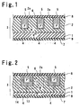
- Fig. 1 is a schematic cross section showing one embodiment of the present invention.
- This semiconductor device has a structure provided with a semiconductor substrate 3, a semiconductor filled material (P - region) 5, a first electrode film (anode electrode film) 8, and a second electrode film (cathode electrode film) 9.
- the semiconductor substrate 3 is constituted by laminating a first semiconductor layer (n-type substrate) 1 of a first conductivity type and a second semiconductor layer (N - epi-layer) 2 of the first conductivity type having a lower impurity concentration than that of the first layer.
- the semiconductor filled material (P - region) 5 is obtained by filling polycrystalline silicon of a second conductivity type up to the same level as the surface of the N - epi-layer 2 in trenches 4 having a prescribed width formed at prescribed intervals in a surface of the N - epi-layer 2 on one main surface side of this semiconductor substrate 3.
- the first electrode film (anode electrode film) 8 is composed of a metal which is brought into contact with both the surface 6 of the N - epi-layer 2 and the surface 7 of the semiconductor filled material 5 and has Schottky junction with the surface 6 of the N - epi-layer 2.
- the second electrode film (cathode electrode film) 9 forms ohmic contact with the n-type substrate 1 on the other main surface of the semiconductor substrate 3.
- the impurity concentration of the semiconductor filled material 5 is so low that the whole semiconductor filled material 5 is depleted when a reverse voltage is applied to the pn junction between the N - epi-layer 2 and the semiconductor filled material 5.
- Figs. 2 and 3 are explanatory views of this embodiment of the invention in operation.
- depletion layers 13, 14 extend from opposed sidewalls 11, 12 of adjacent trenches 4 to the N - epi-region 2a interposed between the trenches 4 and the semiconductor filled material 5 in a lateral direction as shown in Fig. 2 .
- the width W m between the adjacent trenches 4 formed in the surface of the N - epi-layer 2 is preferably a width W m which allows the depletion layers extending from the opposed sidewalls 11, 12 of the adjacent trenches 4 to be connected with each other.
- the width W m which allows the depletion layers extending from the adjacent trenches 4 to be connected with each other means a width W m which also allows the whole N - epi-region 2a interposed between the trenches 4 to be depleted when the whole semiconductor filled material 5 is depleted.
- This width W m is related to the width W t and the concentration N a of the semiconductor filled material 5 formed in the trench 4 and the concentration N d of the N - epi-layer 2a.
- BV AK 60 ⁇ x E g / 1.1 1.5 x N d / 10 16 - 3 / 4
- N d represents an impurity concentration of the second semiconductor layer and its unit is cm -3
- E g represents an energy band gap value of the semiconductor material and its unit is eV
- the width W m of between semiconductor filled materials adjacent to each other formed in the second semiconductor layers satisfies the following equations (1) and (2): W m ⁇ W t ⁇ N ⁇ N ⁇ (where the unit of the width W m is cm; W t represents a width of the semiconductor filled material and its unit is cm; and N a represents an impurity concentration in the semiconductor filled material and its unit is cm -3 )
- the whole N - epi-region 2a is also depleted only under the condition under which these equations (1) and (2) are satisfied. That is, since both the semiconductor filled material 5 and the N - epi-region 2a are depleted, one wide depletion layer 15 connected from the anode electrode film 8 to the bottom of the trench 4 is formed as shown in Fig. 3 . When a reverse voltage is further applied, the voltage applied after formation of this wide depletion layer 15 is generally applied into this wide depletion layer 15. This wide depletion layer 15 is formed by depletion layers extending from the sidewalls 11, 12 of the trenches 4 in the lateral direction.
- the electric field in the depletion layer 15 is still low.
- the electric field strength in the depletion layer 15 is increased as a whole.
- breakdown starts.
- breakdown occurs in the vicinity of the pn junction portion where the electric field strength becomes the highest.
- the electric field strength of the pn junction can be sufficiently relaxed by forming the above-described depletion layer 15.
- the avalanche breakdown voltage may be reached at the center between the adjacent trenches 4 in the N - epi-region 2a interposed between semiconductor filled material 5 before breakdown occurs in the vicinity of the pn junction portion.
- the symbol connecting the left-hand and the right-hand side of the equation (1) means "approximately equal” and used here to include error arisen in manufacture which is within the range that does not affect avalanche breakdown voltage much.
- the equation (1) means that the total amount of the impurities disposed in a region between the adjacent trenches filled with the semiconductor material is approximately equal to the total amount of the impurities in one trench.
- depletion layers extend from two trenches facing to each other and being located at the both sides of the semiconductor material to the semiconductor material interposed between the trenches.
- Equation (2) means that the depletion layers extending from the opposite sides of the semiconductor material come into contact in the semiconductor material disposed in the region interposed between the two trenches facing each other before the reverse bias voltage reaches the avalanche breakdown voltage of the semiconductor material and the avalanche breakdown voltage of the semiconductor filled material.
- Fig. 4 shows the distribution of electric field strengths in a vertical direction along lines A and B, which are located at the centers of the semiconductor filled materials 5 and the N - epi-region 2a interposed between the trenches 4, respectively, when a reverse avalanche breakdown voltage is applied to the semiconductor device in Fig. 1 .
- the electric field strength in the depletion layer 15 is increased as a whole.
- the electric field strength in the depletion layer is increased with the same gradient as when the depletion layers 13 extending from the sidewalls 11, 12 of the trenches 4 are connected and depleted and becomes generally uniform in the depletion layer 15. There is no site where the electric field strength is particularly high.
- the N - epi-layer 2 has such an impurity concentration N d as to allow the depletion layers 13 extending from the sidewalls 11, 12 of the trenches 4 in the lateral direction to be connected, a reverse avalanche breakdown voltage can be increased without lowering the impurity concentration unlike a conventional structure product since the width of the depletion layer 15 can be further increased only by increasing the depth of the trench 4. Therefore, forward characteristics can be greatly improved while the electric field strength applied to the interface between the main surface 6 of the N - epi-layer 2 and the anode electrode film 8 is maintained at the same level as that of a conventional structure product.
- the reverse avalanche breakdown voltage can be determined only by changing the width of the depletion layer 15 extending downward from the anode electrode film 8.
- the reverse avalanche breakdown voltage is determined depending on the depth of the trench 4 having the semiconductor filled material 5 therein. Therefore, when the width W m of the N - epi-region 2a interposed between the trenches 4 and the impurity concentration in the N - epi-layer 2 are set such that the depletion layers 13 extending from the trenches 4 in the lateral direction are connected, medium and high avalanche breakdown voltages can be obtained without lowering the impurity concentration of the N - epi-layer 2 to increase a reverse avalanche breakdown voltage unlike a conventional structure product. That is, there is no increase in leakage current when a reverse voltage is applied and thereby forward characteristics can be greatly improved.
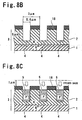
- Figs. 8(a) to 8(d) are cross sections showing processes of fabricating the SBD.
- a silicon oxide film 18 is formed about 5000 x 10 -8 cm on the surface of the N - epi-layer 2 by thermal oxidation. Then, the silicon oxide film 18 is removed with a width W t of about 0.6 ⁇ m and left with a width W m of about 2.4 ⁇ m by photolithography resulting in stripes.
- the silicon oxide film 18 used as a mask for forming trenches 4 is removed by etching.
- Schottky barrier metal is vapor deposited on the surface 6 of the N - epi-layer 2 and the surface 7 of the polycrystalline silicon filled in the trenches 4 to form an anode electrode film 8.
- a cathode electrode film 9 is formed on the other side of the n-type substrate, which is a rear surface, and thus this embodiment of the invention is accomplished as shown in Fig. 8(d) (embodiments of the peripheral structure are omitted).
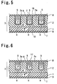
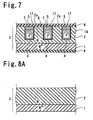
- Figs. 5, 6 and 7 show structures of other embodiments of the invention.
- Fig. 5 is a cross section showing an example where an insulating film 16 is formed on the sidewalls 11, 12 and the bottom surface 10 of the trenches 4 in advance when polycrystalline silicon (semiconductor filled material 5) having a low impurity concentration is filled in the trenches 4 and then a semiconductor filled material 5 is provided.
- This insulating film 16 plays a role of making leakage current almost 0 (zero) when a reverse voltage is applied between the polycrystalline silicon and the N - epi-layer 2.
- Fig. 6 shows an example where a fourth semiconductor region (P ++ region) 17 of the second conductivity type having a high impurity concentration is provided so that the depletion layer 14 extending to the semiconductor filled material 5 when a reverse voltage is applied does not reach the surface 7 of the semiconductor filled material 5.
- This P ++ region 17 can prevent leakage current which occurs because the depletion layer 14 formed upon application of a reverse voltage reaches the anode electrode film 8 brought into contact with the surface 7 of the semiconductor filled material 5 (punch through) and can make the potential of the semiconductor filled material 5 the same as that of the anode electrode film 8 by having ohmic contact with the anode electrode film 8 brought into contact with the surface 7 of the semiconductor filled material 5.
- Fig. 7 shows a combination of the above-described structures, which is an example where an insulating film 16 is formed in the trenches 4 and then a P ++ region 17 is formed on the surface of the semiconductor filled material 5.
- single crystal silicon of the second conductivity type may be formed by epitaxial growth to constitute the semiconductor filled material 5.
- the reverse leakage current which occurs when the semiconductor filled material 5 is constituted by polycrystalline silicon can be reduced by forming p - -type single crystal silicon by epitaxial growth. This structure can also be applied to all the above-described structures.
- a p - region is provided in a trench formed in a surface of an N - epi-layer. Since depletion layers extending from the pn junctions of side surfaces of the trenches are connected with each other in this P - region and the N - epi-layer region interposed between the trenches, a wide depletion layer from the surface to the bottom of the trench can be formed to increase a reverse avalanche breakdown voltage. Therefore, the reverse avalanche breakdown voltage can be increased only by changing the depth of the trench without changing an impurity concentration of the N - epi-layer. Thus, a semiconductor device such as a Schottky barrier diode or the like in which forward characteristics can be greatly improved can be provided without changing reverse characteristics.
Description
- The present invention relates to a semiconductor device, in particular, to a semiconductor device having a Schottky barrier diode structure.
- While a Schottky barrier diode (SBD) has a low forward voltage and a high switching speed, the SBD has high reverse leakage current and a low reverse avalanche breakdown voltage as its disadvantage. In a medium or high voltage product of 100 V or higher, in particular, the reverse leakage current needs to be reduced to prevent thermorunaway. The impurity concentration of a drift region needs to be lowered so that a depletion layer is expanded while maintaining a high Schottky barrier height. As a result, forward characteristics are deteriorated.
-
Fig. 10 shows a structure for reducing leakage current by utilizing a pinch-off effect due to a junction used in a low voltage product. In this figure, an n-type semiconductor layer 2 (hereinafter, referred to as N- epi-layer 2) having a low impurity concentration is formed on an n-type semiconductor substrate 1 (hereinafter, referred to as n-type substrate 1) having a high impurity concentration by epitaxial growth. P-type semiconductor regions 19 (hereinafter, referred to as P+ regions 19) having a high impurity concentration are disposed at prescribed intervals in the main surface of the N- epi-layer 2 by diffusion or embedding of polycrystalline silicon in the trench. Ananode electrode film 8 contacted to themain surface 6 of the N- epi-layer 2 andsurfaces 20 of the P+ regions 19 is formed. Theanode electrode film 8 has Schottky contact with themain surface 6 of the N- epi-layer 2. Acathode electrode film 9 having ohmic contact with the n-type substrate 1 is formed on the other surface of the n-type substrate 1. - When a reverse voltage is gradually applied to an SBD in
Fig. 10 , depletion layers 231 extend from side surfaces 21, 22 of the P+ regions 19 into aregion 2a in the N- epi-layer 2 interposed between the adjacent P+ regions 19 as shown inFig. 11 . When the reverse voltage is further applied, edges of the depletion layers extending from the side surfaces 21, 22 of the P+ regions 19 come into contact with each other (pinch-off) and become one wide depletion layer 232. Therefore, an electric field applied to an interface between themain surface 6 of the N- epi-layer 2 and theanode electrode film 8 is relaxed and thereby reverse leakage current can be reduced. -
Fig. 12 shows a distribution of electric field strengths in a vertical direction along lines A and B, which are located at the centers of the P+ region 19 and the N- epi-region 2a interposed between the P+ regions 19, respectively, when a reverse avalanche breakdown voltage is applied to the semiconductor device in a pinch-off state inFig. 10 . As described above, it is evident fromFig. 12 that an electric field applied to the interface between themain surface 6 of the N- epi-layer 2 and theanode electrode film 8 is relaxed. - However, if the structure shown in
Fig. 10 is applied to a medium or high voltage product of 100 V or higher, an electric field is increased at a pn junction between thebottom 24 of the P+ region 19 and the N- epi-layer 2, leading to deterioration of the reverse avalanche breakdown voltage. To maintain the reverse avalanche breakdown voltage, the impurity concentration of the N- epi-layer 2 needs to be lowered, resulting in deterioration of forward characteristics. - There is also a structure in which only a bottom portion of the P+ region 19 in
Fig. 10 is formed of a p-type semiconductor region 25 having a low impurity concentration to relax the electric field at the bottom of the P+ region 19 as shown inFig. 13 . However, if the impurity concentration of the p-type semiconductor region 25 becomes lower than a desired concentration, an electric field is concentrated at the bottom of the P+ region 19, resulting in deterioration of the reverse avalanche breakdown voltage. If the impurity concentration of the p-type semiconductor region 25 is higher than a desired concentration, an electric field is concentrated at the bottom of the p-type semiconductor region 25, also resulting in deterioration of the reverse avalanche breakdown voltage. - In this structure, a large region having a low impurity concentration needs to be provided at the bottom to sufficiently relax the electric field. However, if a region having a low impurity concentration is further extended to under the p-
type semiconductor region 25, a thickness of the N- epi-layer 2 needs to be increased, resulting in deterioration of forward characteristics, which is a trade-off. - When reverse leakage current is reduced and a reverse avalanche breakdown voltage is maintained in a Schottky barrier diode with a medium or high avalanche breakdown voltage of 100 V or higher to prevent thermorunaway, there exists a trade-off that forward characteristics are deteriorated since the impurity concentration of the N- epi-layer is lowered or a pinch-off effect due to the junction is utilized.
- In view of the foregoing, an object of the present invention is to provide a semiconductor device comprising a Schottky barrier diode in which reverse leakage current is maintained at a conventional level while forward characteristics are greatly improved.
- To achieve the above object, the present invention provides a semiconductor device having a first semiconductor layer composed of a semiconductor of a first conductivity type, a second semiconductor layer of the first conductivity type having a lower impurity concentration than that of the first semiconductor layer, trench portions composed of thin trenches having a prescribed width and prescribed intervals therebetween formed in the second semiconductor layer surface, a semiconductor filled material composed of semiconductor of a second conductivity type, which is opposite to the first conductivity type, filled in the trench portions, a Schottky metal electrode formed on the surface of the second semiconductor layer and the surface of the semiconductor filled material while forming a Schottky junction with the second semiconductor layer and an ohmic contact with the semiconductor filled material, and an ohmic metal electrode formed on the surface of the first semiconductor layer. In this semiconductor device, at least the second semiconductor layer and the semiconductor filled material are constituted by the same semiconductor material. When an avalanche breakdown voltage BVAK between the semiconductor filled material and the second semiconductor layer is expressed by

(where the unit of the width Wm is cm; Wt represents a width

- The present invention also provides a semiconductor device in which an insulating film is formed on the sidewall and the bottom surface of the trench portion and the insulating film is disposed between the semiconductor filled material and the second semiconductor layer.
- The present invention also provides a semiconductor device in which a high impurity concentration layer of the second conductivity type is formed on the surface of the semiconductor filled material.
-
-
Fig. 1 is a schematic cross section showing one embodiment of the invention; -
Fig. 2 is an explanatory view of the embodiment of the invention in operation; -
Fig. 3 is an explanatory view of the embodiment of the invention in operation; -
Fig. 4 is a graph showing characteristics of the electric field strength distribution in the embodiment of the invention; -
Fig. 5 is a schematic cross section showing another embodiment of the invention; -
Fig. 6 is a schematic cross section showing another embodiment of the invention; -
Fig. 7 is a schematic cross section showing another embodiment of the invention; -
Figs. 8(a) to 8(d) are cross sections showing processes of fabricating a device according to one embodiment of the invention; -
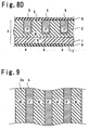
Fig. 9 is a schematic plan view of a device according to the embodiment of the invention; -
Fig. 10 is a schematic cross section of a conventional device; -
Fig. 11 is an explanatory view of the conventional device in operation; -
Fig. 12 is a graph showing characteristics of the electric field strength distribution of the conventional device; and -
Fig. 13 is a schematic cross section of the conventional device. -
Fig. 1 is a schematic cross section showing one embodiment of the present invention. This semiconductor device has a structure provided with asemiconductor substrate 3, a semiconductor filled material (P- region) 5, a first electrode film (anode electrode film) 8, and a second electrode film (cathode electrode film) 9. Thesemiconductor substrate 3 is constituted by laminating a first semiconductor layer (n-type substrate) 1 of a first conductivity type and a second semiconductor layer (N- epi-layer) 2 of the first conductivity type having a lower impurity concentration than that of the first layer. The semiconductor filled material (P- region) 5 is obtained by filling polycrystalline silicon of a second conductivity type up to the same level as the surface of the N- epi-layer 2 intrenches 4 having a prescribed width formed at prescribed intervals in a surface of the N- epi-layer 2 on one main surface side of thissemiconductor substrate 3. The first electrode film (anode electrode film) 8 is composed of a metal which is brought into contact with both thesurface 6 of the N- epi-layer 2 and thesurface 7 of the semiconductor filledmaterial 5 and has Schottky junction with thesurface 6 of the N- epi-layer 2. The second electrode film (cathode electrode film) 9 forms ohmic contact with the n-type substrate 1 on the other main surface of thesemiconductor substrate 3. In this semiconductor device, the impurity concentration of the semiconductor filledmaterial 5 is so low that the whole semiconductor filledmaterial 5 is depleted when a reverse voltage is applied to the pn junction between the N- epi-layer 2 and the semiconductor filledmaterial 5. - This embodiment will be described below with reference to
Figs. 2 and3 .Figs. 2 and3 are explanatory views of this embodiment of the invention in operation. First, when a reverse voltage starts to be applied to the semiconductor device,depletion layers opposed sidewalls 11, 12 ofadjacent trenches 4 to the N- epi-region 2a interposed between thetrenches 4 and the semiconductor filledmaterial 5 in a lateral direction as shown inFig. 2 . When the reverse voltage is further applied, the width Wm between theadjacent trenches 4 formed in the surface of the N- epi-layer 2 is preferably a width Wm which allows the depletion layers extending from theopposed sidewalls 11, 12 of theadjacent trenches 4 to be connected with each other. - The width Wm which allows the depletion layers extending from the
adjacent trenches 4 to be connected with each other means a width Wm which also allows the whole N- epi-region 2a interposed between thetrenches 4 to be depleted when the whole semiconductor filledmaterial 5 is depleted. This width Wm is related to the width Wt and the concentration Na of the semiconductor filledmaterial 5 formed in thetrench 4 and the concentration Nd of the N- epi-layer 2a. When an avalanche breakdown voltage BVAK between the semiconductor filled material and the second semiconductor layer is expressed by


- When the whole semiconductor filled
material 5 is depleted, the whole N- epi-region 2a is also depleted only under the condition under which these equations (1) and (2) are satisfied. That is, since both the semiconductor filledmaterial 5 and the N- epi-region 2a are depleted, onewide depletion layer 15 connected from theanode electrode film 8 to the bottom of thetrench 4 is formed as shown inFig. 3 . When a reverse voltage is further applied, the voltage applied after formation of thiswide depletion layer 15 is generally applied into thiswide depletion layer 15. Thiswide depletion layer 15 is formed by depletion layers extending from thesidewalls 11, 12 of thetrenches 4 in the lateral direction. At the point when the depletion layers 13 extending from thetrenches 4 in the lateral direction are connected, the electric field in thedepletion layer 15 is still low. When the reverse voltage is further applied, the electric field strength in thedepletion layer 15 is increased as a whole. When the electric field strength reaches the critical value, breakdown starts. In case of a reverse avalanche breakdown voltage at the pn junction, breakdown occurs in the vicinity of the pn junction portion where the electric field strength becomes the highest. In the structure of the semiconductor device of the present invention, however, breakdown does not necessarily occur in the vicinity of the pn junction portion. The electric field strength of the pn junction can be sufficiently relaxed by forming the above-describeddepletion layer 15. The avalanche breakdown voltage may be reached at the center between theadjacent trenches 4 in the N- epi-region 2a interposed between semiconductor filledmaterial 5 before breakdown occurs in the vicinity of the pn junction portion. - The impurity concentrations Nd and Na, the width Wt, and the width Wm satisfy the equation Wm=Wt × Nα/Nλ but Wm can not be completely equal to Wt x Nα/Nλ on practically manufactured devices. The symbol connecting the left-hand and the right-hand side of the equation (1) means "approximately equal" and used here to include error arisen in manufacture which is within the range that does not affect avalanche breakdown voltage much.
- As described above, a plurality of straight trenches having an approximate rectangular cross section are arranged in parallel and the equation (1) means that the total amount of the impurities disposed in a region between the adjacent trenches filled with the semiconductor material is approximately equal to the total amount of the impurities in one trench.
- When the semiconductor filled material disposed in the trenches and the semiconductor material disposed in the region interposed between the trenches are reverse biased, depletion layers extend from two trenches facing to each other and being located at the both sides of the semiconductor material to the semiconductor material interposed between the trenches.
- Equation (2) means that the depletion layers extending from the opposite sides of the semiconductor material come into contact in the semiconductor material disposed in the region interposed between the two trenches facing each other before the reverse bias voltage reaches the avalanche breakdown voltage of the semiconductor material and the avalanche breakdown voltage of the semiconductor filled material.
-
Fig. 4 shows the distribution of electric field strengths in a vertical direction along lines A and B, which are located at the centers of the semiconductor filledmaterials 5 and the N- epi-region 2a interposed between thetrenches 4, respectively, when a reverse avalanche breakdown voltage is applied to the semiconductor device inFig. 1 . As described above, the electric field strength in thedepletion layer 15 is increased as a whole. The electric field strength in the depletion layer is increased with the same gradient as when the depletion layers 13 extending from thesidewalls 11, 12 of thetrenches 4 are connected and depleted and becomes generally uniform in thedepletion layer 15. There is no site where the electric field strength is particularly high. Therefore, when the N- epi-layer 2 has such an impurity concentration Nd as to allow the depletion layers 13 extending from thesidewalls 11, 12 of thetrenches 4 in the lateral direction to be connected, a reverse avalanche breakdown voltage can be increased without lowering the impurity concentration unlike a conventional structure product since the width of thedepletion layer 15 can be further increased only by increasing the depth of thetrench 4. Therefore, forward characteristics can be greatly improved while the electric field strength applied to the interface between themain surface 6 of the N- epi-layer 2 and theanode electrode film 8 is maintained at the same level as that of a conventional structure product. - In the structure of the present invention, the reverse avalanche breakdown voltage can be determined only by changing the width of the
depletion layer 15 extending downward from theanode electrode film 8. In other words, the reverse avalanche breakdown voltage is determined depending on the depth of thetrench 4 having the semiconductor filledmaterial 5 therein. Therefore, when the width Wm of the N- epi-region 2a interposed between thetrenches 4 and the impurity concentration in the N- epi-layer 2 are set such that the depletion layers 13 extending from thetrenches 4 in the lateral direction are connected, medium and high avalanche breakdown voltages can be obtained without lowering the impurity concentration of the N- epi-layer 2 to increase a reverse avalanche breakdown voltage unlike a conventional structure product. That is, there is no increase in leakage current when a reverse voltage is applied and thereby forward characteristics can be greatly improved. - A method of fabricating a device of the present invention (Schottky barrier diode) will be described below with reference to
Figs. 8(a) to 8(d). Figs. 8(a) to 8(d) are cross sections showing processes of fabricating the SBD. - First, a
semiconductor substrate 3 is formed by laminating an N- epi-layer 2 (phosphorus concentration Nd = 1 × 10¹⁶ atoms/cm3) having a thickness of about 10 µm on an n-type substrate 1 (arsenic concentration 2 x 10¹⁹ atoms/cm3) by epitaxial growth as shown inFig. 8(a) . - Subsequently, a
silicon oxide film 18 is formed about 5000 x 10-8 cm on the surface of the N- epi-layer 2 by thermal oxidation. Then, thesilicon oxide film 18 is removed with a width Wt of about 0.6 µm and left with a width Wm of about 2.4 µm by photolithography resulting in stripes. By using this film as a mask, silicon of the N- epi-layer 2 is etched with a gas to formtrenches 4 of about 6 µm in depth from the surface of N- epi-layer as shown inFig. 8(b) . At this time, n = 1.42 in the aforementioned equation (2). - Subsequently, polycrystalline silicon into which boron of Na = about 4 x 10¹⁶ atoms/cm3 is doped is deposited about 1 µm on the inner surface of the
trenches 4 and on the surface of thesilicon oxide film 18 as shown inFig. 8(c) and then etched back until its height becomes the same level as the surface of the N- epi-layer 2. - Subsequently, the
silicon oxide film 18 used as a mask for formingtrenches 4 is removed by etching. Schottky barrier metal is vapor deposited on thesurface 6 of the N- epi-layer 2 and thesurface 7 of the polycrystalline silicon filled in thetrenches 4 to form ananode electrode film 8. Acathode electrode film 9 is formed on the other side of the n-type substrate, which is a rear surface, and thus this embodiment of the invention is accomplished as shown inFig. 8(d) (embodiments of the peripheral structure are omitted). -
Figs. 5, 6 and7 show structures of other embodiments of the invention.Fig. 5 is a cross section showing an example where an insulatingfilm 16 is formed on thesidewalls 11, 12 and thebottom surface 10 of thetrenches 4 in advance when polycrystalline silicon (semiconductor filled material 5) having a low impurity concentration is filled in thetrenches 4 and then a semiconductor filledmaterial 5 is provided. This insulatingfilm 16 plays a role of making leakage current almost 0 (zero) when a reverse voltage is applied between the polycrystalline silicon and the N- epi-layer 2. -
Fig. 6 shows an example where a fourth semiconductor region (P++ region) 17 of the second conductivity type having a high impurity concentration is provided so that thedepletion layer 14 extending to the semiconductor filledmaterial 5 when a reverse voltage is applied does not reach thesurface 7 of the semiconductor filledmaterial 5. This P++ region 17 can prevent leakage current which occurs because thedepletion layer 14 formed upon application of a reverse voltage reaches theanode electrode film 8 brought into contact with thesurface 7 of the semiconductor filled material 5 (punch through) and can make the potential of the semiconductor filledmaterial 5 the same as that of theanode electrode film 8 by having ohmic contact with theanode electrode film 8 brought into contact with thesurface 7 of the semiconductor filledmaterial 5. - Furthermore,
Fig. 7 shows a combination of the above-described structures, which is an example where an insulatingfilm 16 is formed in thetrenches 4 and then a P++ region 17 is formed on the surface of the semiconductor filledmaterial 5. - Not polycrystalline silicon, but single crystal silicon of the second conductivity type may be formed by epitaxial growth to constitute the semiconductor filled
material 5. - The reverse leakage current which occurs when the semiconductor filled
material 5 is constituted by polycrystalline silicon can be reduced by forming p--type single crystal silicon by epitaxial growth. This structure can also be applied to all the above-described structures. - As described above, in the present invention, a p- region is provided in a trench formed in a surface of an N- epi-layer. Since depletion layers extending from the pn junctions of side surfaces of the trenches are connected with each other in this P- region and the N- epi-layer region interposed between the trenches, a wide depletion layer from the surface to the bottom of the trench can be formed to increase a reverse avalanche breakdown voltage. Therefore, the reverse avalanche breakdown voltage can be increased only by changing the depth of the trench without changing an impurity concentration of the N- epi-layer. Thus, a semiconductor device such as a Schottky barrier diode or the like in which forward characteristics can be greatly improved can be provided without changing reverse characteristics.
Claims (4)
- A semiconductor device comprising:a first semiconductor layer (1) composed of a semiconductor of a first conductivity type;a second semiconductor layer (2) of the first conductivity type having a lower impurity concentration than that of the first semiconductor layer (1);trench portions composed of thin trenches (4) having a prescribed width and prescribed intervals therebetween formed in the surface (6) of the second semiconductor layer (2), and the trench portions having straight shape and an approximate rectangular cross section;a semiconductor filled material (5) composed of semiconductor of a second conductivity type, which is opposite to the first conductivity type, and filled in the trench portions;a Schottky metal electrode (8) formed on the surface (6) of the second semiconductor layer (2) and the surface (7) of the semiconductor filled material (5), said Schottky metal electrode (8) forming a Schottky junction with the second semiconductor layer (2) and an ohmic contact with the semiconductor filled material (5); andan ohmic metal electrode (9) formed on the surface of the first semiconductor layer (1); said semiconductor device, whereinat least said second semiconductor layer (2) and said semiconductor filled material (5) are constituted by the same semiconductor material;when an avalanche breakdown voltage BVAK between said semiconductor filled material (5) and said second semiconductor layer (2) is expressed by

where the unit of BVAK is V; Nd represents an impurity concentration of the
second semiconductor layer (2) and its unit is cm-3; and Eg represents an energy band gap value of the semiconductor material and its unit is eVX, the width Wm between the semiconductor filled materials (5) adjacent to each other formed in the second semiconductor layer (2) satisfies the following equations (1) and (2):

where the unit of the width Wm is cm; Wt represents a width of the semiconductor filled material (5) and its unit is cm; Na represents an impurity concentration of the semiconductor filled material (5) and its unit is cm-3, and where εs represents a relative permittivity of the semiconductor material; εo represents a permittivity
in vacuum and is 8.85418 × 10⁻¹⁴ F/cm; q represents an elementary electrical charge and is 1.60218 × 10⁻¹⁹ coulomb; and in the equation (2), n > 1. - The semiconductor device according to claim 1, wherein an insulating film is formed on sidewall and bottom surface of the trench portion and the insulating film is disposed between said semiconductor filled material and said second semiconductor layer.
- The semiconductor device according to claim 1, wherein a high impurity concentration layer of the second conductivity type is formed on the surface of the semiconductor filled material.
- The semiconductor device according to claim 2, wherein a high impurity concentration layer of the second conductivity type is formed on the surface of the semiconductor filled material.
Applications Claiming Priority (2)
| Application Number | Priority Date | Filing Date | Title |
|---|---|---|---|
| JP2000097554A JP3860705B2 (en) | 2000-03-31 | 2000-03-31 | Semiconductor device |
| JP2000097554 | 2000-03-31 |
Publications (2)
| Publication Number | Publication Date |
|---|---|
| EP1139433A1 EP1139433A1 (en) | 2001-10-04 |
| EP1139433B1 true EP1139433B1 (en) | 2011-03-23 |
Family
ID=18612164
Family Applications (1)
| Application Number | Title | Priority Date | Filing Date |
|---|---|---|---|
| EP01108152A Expired - Lifetime EP1139433B1 (en) | 2000-03-31 | 2001-03-30 | Semiconductor device having a Schottky barrier diode structure |
Country Status (4)
| Country | Link |
|---|---|
| US (1) | US6404032B1 (en) |
| EP (1) | EP1139433B1 (en) |
| JP (1) | JP3860705B2 (en) |
| DE (1) | DE60144263D1 (en) |
Families Citing this family (34)
| Publication number | Priority date | Publication date | Assignee | Title |
|---|---|---|---|---|
| JP4865166B2 (en) | 2001-08-30 | 2012-02-01 | 新電元工業株式会社 | Transistor manufacturing method, diode manufacturing method |
| US7135718B2 (en) | 2002-02-20 | 2006-11-14 | Shindengen Electric Manufacturing Co., Ltd. | Diode device and transistor device |
| JP3914785B2 (en) | 2002-02-20 | 2007-05-16 | 新電元工業株式会社 | Diode element |
| JP4274771B2 (en) | 2002-10-04 | 2009-06-10 | 新電元工業株式会社 | Semiconductor device |
| US6841825B2 (en) | 2002-06-05 | 2005-01-11 | Shindengen Electric Manufacturing Co., Ltd. | Semiconductor device |
| JP3971670B2 (en) | 2002-06-28 | 2007-09-05 | 新電元工業株式会社 | Semiconductor device |
| WO2004066391A1 (en) * | 2003-01-20 | 2004-08-05 | Mitsubishi Denki Kabushiki Kaisha | Semiconductor device |
| JP4610207B2 (en) * | 2004-02-24 | 2011-01-12 | 三洋電機株式会社 | Semiconductor device and manufacturing method thereof |
| JP4773716B2 (en) | 2004-03-31 | 2011-09-14 | 株式会社デンソー | Manufacturing method of semiconductor substrate |
| FI20055057A (en) * | 2004-05-11 | 2005-11-12 | Artto Aurola | semiconductor device |
| DE102004053760A1 (en) * | 2004-11-08 | 2006-05-11 | Robert Bosch Gmbh | Semiconductor device and method for its production |
| DE102004053761A1 (en) * | 2004-11-08 | 2006-05-18 | Robert Bosch Gmbh | Semiconductor device and method for its production |
| JP2006165013A (en) | 2004-12-02 | 2006-06-22 | Nissan Motor Co Ltd | Semiconductor device and its manufacturing method |
| DE102004059640A1 (en) * | 2004-12-10 | 2006-06-22 | Robert Bosch Gmbh | Semiconductor device and method for its production |
| KR100950232B1 (en) * | 2005-10-06 | 2010-03-29 | 가부시키가이샤 섬코 | Method for manufacturing semiconductor substrate |
| EP1863096B1 (en) * | 2006-05-30 | 2017-07-19 | Nissan Motor Company Limited | Semiconductor device and method of manufacturing the same |
| CN101083280B (en) * | 2006-06-01 | 2010-09-22 | 日产自动车株式会社 | Semiconductor device and method for producing the same |
| JP4599379B2 (en) * | 2007-08-31 | 2010-12-15 | 株式会社東芝 | Trench gate type semiconductor device |
| DE102007045185A1 (en) | 2007-09-21 | 2009-04-02 | Robert Bosch Gmbh | Semiconductor device and method for its production |
| US7750412B2 (en) * | 2008-08-06 | 2010-07-06 | Fairchild Semiconductor Corporation | Rectifier with PN clamp regions under trenches |
| TW201015718A (en) | 2008-10-03 | 2010-04-16 | Sanyo Electric Co | Semiconductor device and method for manufacturing the same |
| JP5566020B2 (en) * | 2008-12-22 | 2014-08-06 | 新電元工業株式会社 | Manufacturing method of trench Schottky barrier diode |
| DE102009028252A1 (en) * | 2009-08-05 | 2011-02-10 | Robert Bosch Gmbh | A semiconductor device |
| JP5600411B2 (en) * | 2009-10-28 | 2014-10-01 | 三菱電機株式会社 | Silicon carbide semiconductor device |
| DE102011087591A1 (en) * | 2011-12-01 | 2013-06-06 | Robert Bosch Gmbh | High-voltage trench junction barrier Schottky |
| CN103681778B (en) * | 2012-09-09 | 2017-04-26 | 朱江 | Groove charge compensation schottky semiconductor device and preparation method thereof |
| CN104124151B (en) * | 2014-07-14 | 2017-08-25 | 中航(重庆)微电子有限公司 | A kind of groove structure Schottky-barrier diode and preparation method thereof |
| CN106340453A (en) * | 2015-07-07 | 2017-01-18 | 北大方正集团有限公司 | Diode preparation method and diode |
| CN105023953A (en) * | 2015-07-10 | 2015-11-04 | 淄博汉林半导体有限公司 | Vertical field effect diode and manufacture method thereof |
| JP6678549B2 (en) * | 2016-09-27 | 2020-04-08 | 株式会社 日立パワーデバイス | Semiconductor device, method of manufacturing the same, and power conversion system |
| CN107275221A (en) * | 2017-06-30 | 2017-10-20 | 上海华虹宏力半导体制造有限公司 | The manufacture method of super-junction device |
| CN107275222A (en) * | 2017-06-30 | 2017-10-20 | 上海华虹宏力半导体制造有限公司 | The manufacture method of super-junction device |
| JP7237772B2 (en) * | 2019-08-20 | 2023-03-13 | 株式会社東芝 | semiconductor equipment |
| CN111326567A (en) * | 2020-03-06 | 2020-06-23 | 上海瞻芯电子科技有限公司 | Super junction manufacturing method and super junction Schottky diode thereof |
Family Cites Families (11)
| Publication number | Priority date | Publication date | Assignee | Title |
|---|---|---|---|---|
| JP2667477B2 (en) * | 1988-12-02 | 1997-10-27 | 株式会社東芝 | Schottky barrier diode |
| JPH02154464A (en) * | 1988-12-06 | 1990-06-13 | Fuji Electric Co Ltd | Schottky barrier diode |
| JPH065736B2 (en) * | 1989-12-15 | 1994-01-19 | 株式会社東芝 | Schottky diode |
| CN1019720B (en) | 1991-03-19 | 1992-12-30 | 电子科技大学 | Power semiconductor device |
| US5241195A (en) | 1992-08-13 | 1993-08-31 | North Carolina State University At Raleigh | Merged P-I-N/Schottky power rectifier having extended P-I-N junction |
| JP2809253B2 (en) | 1992-10-02 | 1998-10-08 | 富士電機株式会社 | Injection control type Schottky barrier rectifier |
| JPH06163878A (en) * | 1992-11-24 | 1994-06-10 | Fuji Electric Co Ltd | Semiconductor device |
| DE4309764C2 (en) | 1993-03-25 | 1997-01-30 | Siemens Ag | Power MOSFET |
| JPH08204210A (en) * | 1995-01-20 | 1996-08-09 | Rohm Co Ltd | Schottky barrier diode |
| US6252288B1 (en) * | 1999-01-19 | 2001-06-26 | Rockwell Science Center, Llc | High power trench-based rectifier with improved reverse breakdown characteristic |
| AU5154300A (en) * | 1999-05-28 | 2000-12-18 | Advanced Power Devices, Inc. | Discrete schottky diode device with reduced leakage current |
-
2000
- 2000-03-31 JP JP2000097554A patent/JP3860705B2/en not_active Expired - Fee Related
-
2001
- 2001-03-30 US US09/820,837 patent/US6404032B1/en not_active Expired - Lifetime
- 2001-03-30 EP EP01108152A patent/EP1139433B1/en not_active Expired - Lifetime
- 2001-03-30 DE DE60144263T patent/DE60144263D1/en not_active Expired - Lifetime
Also Published As
| Publication number | Publication date |
|---|---|
| JP2001284604A (en) | 2001-10-12 |
| US6404032B1 (en) | 2002-06-11 |
| EP1139433A1 (en) | 2001-10-04 |
| DE60144263D1 (en) | 2011-05-05 |
| JP3860705B2 (en) | 2006-12-20 |
Similar Documents
| Publication | Publication Date | Title |
|---|---|---|
| EP1139433B1 (en) | Semiconductor device having a Schottky barrier diode structure | |
| EP1168455B1 (en) | Power semiconductor switching element | |
| US6677643B2 (en) | Super-junction semiconductor device | |
| US5262669A (en) | Semiconductor rectifier having high breakdown voltage and high speed operation | |
| US7781869B2 (en) | Semiconductor device having rectifying action | |
| EP1314207B1 (en) | Trench schottky rectifier | |
| US6639278B2 (en) | Semiconductor device | |
| US8035158B2 (en) | Semiconductor device | |
| US6740951B2 (en) | Two-mask trench schottky diode | |
| US20050006699A1 (en) | Semiconductor device and its manufacturing method | |
| US10164087B2 (en) | Semiconductor device and method of manufacturing same | |
| EP1485940B1 (en) | Silicon carbide bipolar junction transistor with overgrown base region | |
| CN109509795B (en) | Silicon carbide schottky device with composite groove structure and manufacturing method thereof | |
| US5345100A (en) | Semiconductor rectifier having high breakdown voltage and high speed operation | |
| US6558984B2 (en) | Trench schottky barrier rectifier and method of making the same | |
| JP2003142698A (en) | Power semiconductor device | |
| US20150155279A1 (en) | Semiconductor Device with Bipolar Junction Transistor Cells | |
| DE102014109208A1 (en) | LOAD COMPENSATION DEVICE AND ITS MANUFACTURE | |
| EP1947699A1 (en) | Trench gate power mosfet | |
| CN110176497B (en) | Silicon carbide semiconductor device and method for manufacturing silicon carbide semiconductor device | |
| CN114530504A (en) | High-threshold SiC MOSFET device and manufacturing method thereof | |
| EP3780071B1 (en) | Semiconductor device and method for manufacturing same | |
| EP4297100A1 (en) | Method for producing a semiconductor device and semiconductor device | |
| US20230006038A1 (en) | Method for forming a drift region of a superjunction device | |
| EP3916797A1 (en) | Semiconductor device and manufacturing method thereof |
Legal Events
| Date | Code | Title | Description |
|---|---|---|---|
| PUAI | Public reference made under article 153(3) epc to a published international application that has entered the european phase |
Free format text: ORIGINAL CODE: 0009012 |
|
| AK | Designated contracting states |
Kind code of ref document: A1 Designated state(s): AT BE CH CY DE DK ES FI FR GB GR IE IT LI LU MC NL PT SE TR Kind code of ref document: A1 Designated state(s): DE FR GB |
|
| AX | Request for extension of the european patent |
Free format text: AL;LT;LV;MK;RO;SI |
|
| 17P | Request for examination filed |
Effective date: 20011108 |
|
| RIN1 | Information on inventor provided before grant (corrected) |
Inventor name: MIZUE, KITADA SHINDENGEN ELECTRIC Inventor name: SHINJI, KUNORI SHINDENGEN ELECTRIC |
|
| AKX | Designation fees paid |
Free format text: DE FR GB |
|
| GRAP | Despatch of communication of intention to grant a patent |
Free format text: ORIGINAL CODE: EPIDOSNIGR1 |
|
| GRAS | Grant fee paid |
Free format text: ORIGINAL CODE: EPIDOSNIGR3 |
|
| GRAA | (expected) grant |
Free format text: ORIGINAL CODE: 0009210 |
|
| AK | Designated contracting states |
Kind code of ref document: B1 Designated state(s): DE FR GB |
|
| REG | Reference to a national code |
Ref country code: GB Ref legal event code: FG4D |
|
| REF | Corresponds to: |
Ref document number: 60144263 Country of ref document: DE Date of ref document: 20110505 Kind code of ref document: P |
|
| REG | Reference to a national code |
Ref country code: DE Ref legal event code: R096 Ref document number: 60144263 Country of ref document: DE Effective date: 20110505 |
|
| PLBE | No opposition filed within time limit |
Free format text: ORIGINAL CODE: 0009261 |
|
| STAA | Information on the status of an ep patent application or granted ep patent |
Free format text: STATUS: NO OPPOSITION FILED WITHIN TIME LIMIT |
|
| 26N | No opposition filed |
Effective date: 20111227 |
|
| REG | Reference to a national code |
Ref country code: DE Ref legal event code: R097 Ref document number: 60144263 Country of ref document: DE Effective date: 20111227 |
|
| REG | Reference to a national code |
Ref country code: FR Ref legal event code: PLFP Year of fee payment: 16 |
|
| REG | Reference to a national code |
Ref country code: FR Ref legal event code: PLFP Year of fee payment: 17 |
|
| PGFP | Annual fee paid to national office [announced via postgrant information from national office to epo] |
Ref country code: FR Payment date: 20170323 Year of fee payment: 17 |
|
| PGFP | Annual fee paid to national office [announced via postgrant information from national office to epo] |
Ref country code: GB Payment date: 20170327 Year of fee payment: 17 |
|
| PGFP | Annual fee paid to national office [announced via postgrant information from national office to epo] |
Ref country code: DE Payment date: 20170329 Year of fee payment: 17 |
|
| REG | Reference to a national code |
Ref country code: DE Ref legal event code: R119 Ref document number: 60144263 Country of ref document: DE |
|
| GBPC | Gb: european patent ceased through non-payment of renewal fee |
Effective date: 20180330 |
|
| PG25 | Lapsed in a contracting state [announced via postgrant information from national office to epo] |
Ref country code: DE Free format text: LAPSE BECAUSE OF NON-PAYMENT OF DUE FEES Effective date: 20181002 |
|
| PG25 | Lapsed in a contracting state [announced via postgrant information from national office to epo] |
Ref country code: GB Free format text: LAPSE BECAUSE OF NON-PAYMENT OF DUE FEES Effective date: 20180330 |
|
| PG25 | Lapsed in a contracting state [announced via postgrant information from national office to epo] |
Ref country code: FR Free format text: LAPSE BECAUSE OF NON-PAYMENT OF DUE FEES Effective date: 20180331 |