EP1139108A2 - Abtastschnittstelle mit Zeitmultiplexmerkmal zur Signalüberlagerung - Google Patents
Abtastschnittstelle mit Zeitmultiplexmerkmal zur Signalüberlagerung Download PDFInfo
- Publication number
- EP1139108A2 EP1139108A2 EP01200790A EP01200790A EP1139108A2 EP 1139108 A2 EP1139108 A2 EP 1139108A2 EP 01200790 A EP01200790 A EP 01200790A EP 01200790 A EP01200790 A EP 01200790A EP 1139108 A2 EP1139108 A2 EP 1139108A2
- Authority
- EP
- European Patent Office
- Prior art keywords
- signal
- signals
- scan interface
- scan
- interface
- Prior art date
- Legal status (The legal status is an assumption and is not a legal conclusion. Google has not performed a legal analysis and makes no representation as to the accuracy of the status listed.)
- Granted
Links
Images


Classifications
-
- G—PHYSICS
- G06—COMPUTING; CALCULATING OR COUNTING
- G06F—ELECTRIC DIGITAL DATA PROCESSING
- G06F11/00—Error detection; Error correction; Monitoring
- G06F11/22—Detection or location of defective computer hardware by testing during standby operation or during idle time, e.g. start-up testing
- G06F11/26—Functional testing
- G06F11/261—Functional testing by simulating additional hardware, e.g. fault simulation
-
- G—PHYSICS
- G01—MEASURING; TESTING
- G01R—MEASURING ELECTRIC VARIABLES; MEASURING MAGNETIC VARIABLES
- G01R31/00—Arrangements for testing electric properties; Arrangements for locating electric faults; Arrangements for electrical testing characterised by what is being tested not provided for elsewhere
- G01R31/28—Testing of electronic circuits, e.g. by signal tracer
- G01R31/317—Testing of digital circuits
- G01R31/31705—Debugging aspects, e.g. using test circuits for debugging, using dedicated debugging test circuits
-
- G—PHYSICS
- G01—MEASURING; TESTING
- G01R—MEASURING ELECTRIC VARIABLES; MEASURING MAGNETIC VARIABLES
- G01R31/00—Arrangements for testing electric properties; Arrangements for locating electric faults; Arrangements for electrical testing characterised by what is being tested not provided for elsewhere
- G01R31/28—Testing of electronic circuits, e.g. by signal tracer
- G01R31/317—Testing of digital circuits
- G01R31/3181—Functional testing
- G01R31/3185—Reconfiguring for testing, e.g. LSSD, partitioning
- G01R31/318505—Test of Modular systems, e.g. Wafers, MCM's
-
- G—PHYSICS
- G06—COMPUTING; CALCULATING OR COUNTING
- G06F—ELECTRIC DIGITAL DATA PROCESSING
- G06F1/00—Details not covered by groups G06F3/00 - G06F13/00 and G06F21/00
- G06F1/22—Means for limiting or controlling the pin/gate ratio
-
- G—PHYSICS
- G06—COMPUTING; CALCULATING OR COUNTING
- G06F—ELECTRIC DIGITAL DATA PROCESSING
- G06F11/00—Error detection; Error correction; Monitoring
- G06F11/22—Detection or location of defective computer hardware by testing during standby operation or during idle time, e.g. start-up testing
- G06F11/26—Functional testing
- G06F11/273—Tester hardware, i.e. output processing circuits
- G06F11/2733—Test interface between tester and unit under test
-
- G—PHYSICS
- G06—COMPUTING; CALCULATING OR COUNTING
- G06F—ELECTRIC DIGITAL DATA PROCESSING
- G06F11/00—Error detection; Error correction; Monitoring
- G06F11/30—Monitoring
- G06F11/34—Recording or statistical evaluation of computer activity, e.g. of down time, of input/output operation ; Recording or statistical evaluation of user activity, e.g. usability assessment
- G06F11/3466—Performance evaluation by tracing or monitoring
Definitions
- the invention relates generally to electronic data processing and, more particularly, to emulation, simulation and test capabilities of electronic data processing devices and systems.
- Advanced wafer lithography and surface-mount packaging technology are integrating increasingly complex functions at both the silicon and printed circuit board level of electronic design. Diminished physical access is an unfortunate consequence of denser designs and shrinking interconnect pitch. Designed-in testability is needed, so that the finished product is still both controllable and observable during test and debug. Any manufacturing defect is preferably detectable during final test before a product is shipped. This basic necessity is difficult to achieve for complex designs without taking testability into account in the logic design phase, so that automatic test equipment can test the product.
- testability circuitry, system and methods that are consistent with a concept of design-for-reusability.
- subsequent devices and systems can have a low marginal design cost for testability, simulation and emulation by reusing the testability, simulation and emulation circuitry, systems and methods that are implemented in an initial device.
- a proactive testability, simulation and emulation approach a large of subsequent design time is expended on test pattern creation and upgrading.
- IC design for example, are accompanied by decreased internal visibility and control, reduced fault coverage and reduced ability to toggle states, more test development and verification problems, increased complexity of design simulation and continually increasing cost of CAD (computer aided design) tools.
- the side effects include decreased register visibility and control, complicated debug and simulation in design verification, loss of conventional emulation due to loss of physical access by packaging many circuits in one package, increased routing complexity on the board, increased costs of design tools, mixed-mode packaging, and design for produceability.
- some side effects are decreased visibility of states, high speed emulation difficulties, scaled time simulation, increased debugging complexity, and increased costs of emulators.
- Production side effects involve decreased visibility and control, complications in test vectors and models, increased test complexity, mixed-mode packaging, continually increasing costs of automatic test equipment even into the 7-figure range, and tighter tolerances.
- Emulation technology utilizing scan based emulation and multiprocessing debug was introduced over 10 years ago.
- the change from conventional in circuit emulation to scan based emulation was motivated by design cycle time pressures and newly available space for on-chip emulation.
- Design cycle time pressure was created by three factors: higher integration levels - such as on-chip memory; increasing clock rates -caused electrical intrusiveness by emulation support logic; and more sophisticated packaging - created emulator connectivity issues.
- On-chip, debug facilities are more affordable than ever before.
- the system cost associated with the random logic accompanying the CPU and memory subsystems is dropping as a percentage of total system cost.
- the cost of a several thousand gates is at an all time low, and can in some cases be tucked into a corner of today's chip designs.
- Cost per pin in today's high density packages has also dropped, making it easier to allocate more pins for debug.
- the combination of affordable gates and pins enables the deployment of new, on-chip emulation facilities needed to address the challenges created by systems-on-a-chip.
- the emulation technology of the present invention uses the debug upside opportunities noted above to provide developers with an arsenal of debug capability aimed at narrowing the control and visibility gap.
- This emulation technology delivers solutions to the complex debug problems of today's highly integrated embedded real-time systems. This technology attacks the loss of visibility, control, and ease of use issues described in the preceding section while expanding the feature set of current emulators.
- the on-chip debug component of the present invention provides a means for optimizing the cost and debug capabilities.
- the architecture allows for flexible combinations of emulation components or peripherals tailored to meet system cost and time to market constraints.
- the scalability aspect makes it feasible to include them in production devices with manageable cost and limited performance overhead.
- Emulation, debug, and simulation tools of the present invention are described herein.
- the emulation and debug solutions described herein are based on the premise that, over time, some if not most debug functions traditionally performed off chip must be integrated into the production device if they are to remain in the developer's debug arsenal.
- the present invention provides a powerful and scalable portfolio of debug capabilities for on-chip deployment. This technology preserves all the gains of initial JTAG technology while adding capabilities that directly assault the visibility, control, and ease of use issues created by the vanishing visibility trend.
- Real-Time Emulation provides a base set of fixed capabilities for real-time execution control (run, step, halt, etc.) and register/memory visibility. This component allows the user to debug application code while real-time interrupts continue to be serviced. Registers and memory may be accessed in real-time with no impact to interrupt processing. Users may distinguish between real-time and non real-time interrupts, and mark code that must not be disturbed by real-time debug memory accesses.
- This base emulation capability includes hardware that can be configured as two single point hardware breakpoints, a single data watchpoint, an event counter, or a data logging mechanism.
- the EMU pin capability includes trigger I/Os for multiprocessor event processing and a uni-directional (target to host) data logging mechanism.
- RTDXTM provides real-time data transfers between an emulator host and target application. This component offers both bi-directional and uni-directional DSP target/host data transfers facilitated by the emulator.
- the DSP (or target) application may collect target data to be transferred to the host or receive data from the host, while emulation hardware (within the DSP and the emulator) manages the actual transfer.
- emulation hardware within the DSP and the emulator
- Trace is a non-intrusive mechanism of providing visibility of the application activity. Trace is used to monitor CPU related activity such as program flow and memory accesses, system activity such as ASIC state machines, data streams and CPU collected data. Historical trace technology also used logic analyzer like collection and special emulation (SEs) devices with more pins than a production device. The logic analyzer or like device processed native representations of the data using a state machine like programming interface (filter mechanism). This trace model relied on all activity being exported with external triggering selecting the data that needed to be stored, viewed and analyzed.
- SEs special emulation
- On-chip Trace with high speed serial data export, in combination with Advanced Analysis provides a solution for SOC designs. Trace is used to monitor CPU related activity such as program flow and memory accesses, system activity such as ASIC state machines, data streams etc. and CPU collected data. This creates four different classes of trace data:
- Collection mechanisms for the four classes of trace data are modular allowing the trade off of functionality verses gates and pins required to meet desired bandwidth requirements.
- the RTDX and Trace functions provide similar, but different forms of visibility. They differ in terms of how data is collected, and the circumstances under which they would be most effective. A brief explanation is included below for clarity:
- RTDXTM Real Time Data eXchange
- RTDX can be used to record the input or output buffers from a DSP algorithm.
- RTDX requires CPU assistance in collecting data hence there is definite, but small, CPU bandwidth required to accomplish this.
- RTDX is an application intrusive mechanism of providing visibility with low recurring overhead cost.
- Trace is a non-intrusive, hardware-assisted collection mechanism (such as, bus snoopers) with very high bandwidth (BW) data export. Trace is used when there is a need to export data at a very high data rate or when the behavior of the information to be traced is not known, or is random in nature or associated with an address. Program flow is a typical example where it is not possible to know the behavior a priori. The bandwidth required to export this class of information is high. Data trace of specified addresses is another example. The bandwidth required to export data trace is very high.
- Trace data is unidirectional, going from target to host only.
- RTDX can exchange data in either direction although unidirectional forms of RTDX are supported (data logging).
- the Trace data path can also be used to provide very high speed uni-directional RTDX (CPU collected trace data).
- Advanced analysis provides a non-intrusive on-chip event detection and trigger generation mechanism.
- the trigger outputs created by advanced analysis control other infrastructure components such as Trace and RTDX.
- Historical trace technology used bus activity exported to a logic analyzer to generate triggers that controlled trace within the logic analyzer unit or generated triggers which were supplied to the device to halt execution. This usually involved a chip that had more pins than the production device (an SE or special emulation device).
- This analysis model does not work well in the System-on-a-Chip (SOC) era as the integration levels and clock rates of today's devices preclude full visibility bus export.
- SOC System-on-a-Chip
- Advanced analysis provides affordable on-chip instruction and data bus comparators, sequencers and state machines, and event counters to recreate the most important portions of the triggering function historically found off chip.
- Advanced analysis provides the control aspect of debug triggering mechanism for Trace, RTDX and Real-Time Emulation. This architectural component identifies events, tracks event sequences, and assigns actions based on their occurrence (break execution, enable/disable trace, count, enable/disable RTDX, etc.).
- the modular building blocks for this capability include bus comparators, external event generators, state machines or state sequencers, and trigger generators.
- the modularity of the advanced analysis system allows the trade off of functionality versus gates.
- Emulator capability is created by the interaction of four emulator components:
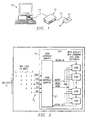
- the host computer 10 is connected to an emulation controller 12 (external to the host) with the emulation controller (also referred to herein as the emulator or the controller) also connected to the target system 16.
- the user preferably controls the target application through a debugger application program, running on the host computer, for example, Texas Instruments' Code Composer Studio program.
- FIG. 1 A typical debug system is shown in Figure 1.
- This system uses a host computer 10 (generally a PC) to access the debug capabilities through an emulator 12.
- the debugger application program presents the debug capabilities in a user-friendly form via the host computer.
- the debug resources are allocated by debug software on an as needed basis, relieving the user of this burden.
- Source level debug utilizes the debug resources, hiding their complexity from the user.
- the debugger together with the on-chip Trace and triggering facilities provide a means to select, record, and display chip activity of interest. Trace displays are automatically correlated to the source code that generated the trace log.
- the emulator provides both the debug control and trace recording function.
- the debug facilities are programmed using standard emulator debug accesses through the target chips' JTAG or similar serial debug interface. Since pins are at a premium, the technology provides for the sharing of the debug pin pool by trace, trigger, and other debug functions with a small increment in silicon cost. Fixed pin formats are also supported. When the sharing of pins option is deployed, the debug pin utilization is determined at the beginning of each debug session (before the chip is directed to run the application program), maximizing the trace export bandwidth. Trace bandwidth is maximized by allocating the maximum number of pins to trace.
- the debug capability and building blocks within a system may vary.
- the emulator software therefore establishes the configuration at run-time. This approach requires the hardware blocks to meet a set of constraints dealing with configuration and register organization.
- Other components provide a hardware search capability designed to locate the blocks and other peripherals in the system memory map.
- the emulator software uses a search facility to locate the resources. The address where the modules are located and a type ID uniquely identifies each block found. Once the IDs are found, a design database may be used to ascertain the exact configuration and all system inputs and outputs.
- the host computer is generally a PC with at least 64 Mbytes of memory and capable of running at least Windows95, SR-2, Windows NT, or later versions of Windows.
- the PC must support one of the communications interfaces required by the emulator, for example:
- the emulation controller 12 provides a bridge between the host computer 10 and target system 16, handling all debug information passed between the debugger application running on the host computer and a target application executing on a DSP (or other target processor) 14.
- One exemplary emulator configuration supports all of the following capabilities:
- emulator-to-target interface supports:
- the emulation controller 12 accesses Real-time Emulation capabilities (execution control, memory, and register access) via a 3, 4, or 5 bit scan based interface.
- RTDX capabilities can be accessed by scan or by using three higher bandwidth RTDX formats that use direct target-to-emulator connections other than scan.
- the input and output triggers allow other system components to signal the chip with debug events and vice-versa.
- the emulator 12 is partitioned into communication and emulation sections.
- the communication section supports communication with the host 10 on host communication links while the emulation section interfaces to the target, managing target debug functions and the device debug port.
- the emulator 12 communicates with the host computer 10 using e.g., one of the aforementioned industry standards communication links at 15.
- the host-to-emulator connection can be established with off the shelf cabling technology. Host-to-emulator separation is governed by the standards applied to the interface used.
- the emulation controller 12 communicates with the target system 16 through a target cable or cables at 17.
- Debug, Trace, Triggers, and RTDX capabilities share the target cable, and in some cases, the same device pins. More than one target cable may be required when the target system deploys a trace width that cannot be accommodated in a single cable. All trace, RTDX, and debug communication occurs over this link.
- FIGURE 2 diagrammatically illustrates pertinent portions of exemplary embodiments of the emulation system of FIGURE 1.
- FIGURE 2 includes a scan interface provided in the cable 17 between the emulator 12 and the target chip 14.
- the emulator 12 can select any one of a plurality of modes of operation for the scan interface.
- the scan interface is a standard JTAG scan interface, but the invention is also applicable to other types of scan interfaces.
- mode J_5 represents the standard JTAG format which utilizes five pins of the target chip.
- Modes J_4 and J_3 designate modes of scan operation wherein time division multiplexing is utilized to combine two or more of the five JTAG signals on a single pin of the scan interface, thereby freeing one or more of the five pins normally associated with standard J_5 operation.
- Mode J_4 multiplexes two JTAG signals onto a single pin, and thus requires four pins for scan operation, thus freeing one pin for other purposes such as other debug functions.
- Mode J_3 multiplexes three JTAG signals onto a single pin, and thus requires only three pins for scan operation, thereby freeing two pins for other purposes such as other debug operations.
- mode J_1 no multiplexing is used, but only the TRST (test logic reset) signal remains dedicated to the scan interface, thereby freeing four pins for other purposes such as debug operation.
- FIGURE 3 provides a description of each of the above-described modes of scan operation. Note that the J_1, J_4 and J_3 modes are limited to point-to-point connections between the emulator and a single target device, while J_5 is of course applicable to any number of scan-chained target devices.
- the target chip includes a scan interface adapter 21 which is responsible for converting the signals received from the emulator, according to any of modes J_5, J_4 or J_3, into a five signal interface identical to the J_5 format, in this example, the five pin JTAG interface.
- signal MSCAN IN corresponds to TDI of the J_5 interface.
- Signal MTRST corresponds to signal TRST of the J_5 interface.
- Signal MTCK corresponds to signal TCK of the J_5 interface.
- Signal MTMS corresponds to signal TMS of the J_5 interface, and signal MSCAN OUT corresponds to signal TDO of the J_5 interface.
- the scan interface adapter 21 translates this interface into, in this example, a five signal JTAG interface for test control of a plurality of cores embedded within the target chip. Conversely, the scan interface adapter 21 converts the five signal interface used within the chip into the signaling format required by the scan interface mode that has been selected on the emulator side.
- FIGURE 4 diagrammatically illustrates the scan interface signaling connections between the emulator and the target chip during J_4 operation.
- the emulator TDO-to-chip TDI connection is used to multiplex both the TMS signal from the emulator and the TDO signal from the emulator.
- TDM time division multiplexed
- the scan interface adapter within the target device then converts from the four pin interface to the standard five signal JTAG format as described above with respect to FIGURE 2.
- the TMS signaling path between the target device and the emulator is free for other purposes such as debug functions.
- FIGURE 5 illustrates the scan interface connections between the emulator and a target chip when the J_3 scan format is used.
- the emulator TDI-to-chip TDO connection is used as a bi-directional signal on which the TMS signal from the emulator, the TDO signal from the emulator and the TDI signal from the target chip are time division multiplexed.
- this configuration frees two connections between the emulator and the target chip (TMS and target TDI-to-emulator TDO) for other purposes such as debug functions.
- the aforementioned J_1 configuration permits four of the five scan interface connections to be used for other purposes such as debug functions, and the scan interface retains control of only the TRST connection so that the emulator can still selectively configure the scan interface 21 adapter for scan operations (which are of course not possible in the J_1 configuration).
- the assertion of TRST by the emulator causes the scan interface adapter 21 to set the scan interface to a default scan interface setting, for example J_3, J_4 or J_5.
- the default setting can be specified by the chip architect, and the emulator software can easily be made compatible with any choice of default operation.
- FIGURE 6 illustrates exemplary operations which can be performed by the scan interface adapter and emulator in the J_4 mode.
- a state machine within the emulator controls the input and output sequence for the J_4 interface configuration.
- the state machine includes nine states to control J_4 input and output.
- the state sequence begins with a start bit, followed by four TMS values, followed by four TDI values.
- the scan interface adapter in the target device also includes a state machine which is operable to convert the J_4 interface to the J_5 interface, including enabling the signal MTCK of FIGURE 2 during only four states (0x4, 0x5, 0x6 and 0x7) of the nine state sequence, which four states are used for TDO output from the target to the emulator and parallel TMS/TDI output from the scan interface adaptor to the cores.
- a state machine which is operable to convert the J_4 interface to the J_5 interface, including enabling the signal MTCK of FIGURE 2 during only four states (0x4, 0x5, 0x6 and 0x7) of the nine state sequence, which four states are used for TDO output from the target to the emulator and parallel TMS/TDI output from the scan interface adaptor to the cores.
- the state machine within the chip's scan interface adapter is forced to a start state (0xF).
- the state machine can also be forced into the start state, in some embodiments, if the emulator's TDO signal is a logic 1 for a least 9 consecutive cycles of TCK when TCK is running continuously.
- the scan interface adapter While the scan interface adapter is in the start state, if it detects a logic 1 on its TDI input, it asserts test reset (MTRST in FIGURE 2) to the cores of the target chip, and remains in the start state.
- the state machine When the scan interface adapter detects a 0 on its TDI input while in the start state, the state machine begins the state progression illustrated in FIGURE 6, progressing sequentially from state 0x0 to state 0x7, and then to the start state 0xF, where it again performs the check for a logic 0 on its TDI input.
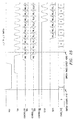
- FIGURE 7 is a timing diagram which corresponds to the J_4 operations illustrated in FIGURE 6.
- FIGURE 8 illustrates exemplary operations which can be performed by the emulator and scan interface adapter in the J_3 scan mode.
- the scan interface adapter initializes its state machine to the reset state when the emulator supplies at least sixteen clocks (TCK) while a logic 1 is supplied by the emulator to the TDO pin of the target device.
- the state machine within the emulator cooperates with the adapter state machine, using sixteen states to manage the J_3 scan operation.
- the state sequence begins with the emulator sending from its TDI pin to the TDO pin of the target device a start bit (0) followed by four TMS values, followed by four TDI values.
- the emulator ceases to drive the TDO pin of the target device.
- neither the emulator nor the target device is driving the TDO pin of the target device.
- the target device drives its TDO pin for the first of five TCK cycles. During the first four of these TCK cycles, the target device drives out target device scan data TDO_0 - TDO_3.
- the signal MTCK of FIGURE 2 is enabled only during these four states, to permit parallel TMS/TDI output from the scan interface adaptor to the cores.
- the target device drives its TDO pin value to logic 1 as illustrated at 83.
- the target device Upon the next TCK pulse at 84, the target device relinquishes control of its TDO pin to the emulator, and the emulator drives logic 1. Because both the emulator and the target device are driving a logic 1 when control is exchanged at 84, there is no bus conflict during this exchange of control. During the next TCK cycle, the emulator applies the start bit to begin the FIGURE 8 sequence again.
- the state machine of the target device is forced to state 0xF when the TRST pin is driven to 0.
- the target device state machine expects the emulator to supply the logic 0 start bit. Failure to detect the start bit means the emulator and target have lost synchronization, the emulator is not present, or the emulator and target are operating in different scan interface modes. If the target device state machine detects a logic 1 during the 0xF state, then the state machine of the target device asserts MTRST to the internal cores of the target device, and remains in the state 0xF.
- the target device state machine When a 0 is detected on the target device TDO input with the target device state machine in state 0xF, the target device state machine begins its state progression, progressing sequentially from state 0x0 through 0xE, and then to state 0xF where it again performs the aforementioned check for a logic 0 start bit on its TDO pin.
- the emulator applies a continuously running TCK and the TDO pin of the target device is pulled up to a logic 1
- the state machine within the scan interface adapter of the target device initializes to the test reset condition within sixteen TCK cycles when TRST is not asserted during the period that TDO is pulled up to logic 1 with a continuously running TCK.
- FIGURE 9 is a timing diagram which corresponds to the J_3 operations of FIGURE 8.
- the selected scan interface mode i.e. J_5, J_4, J_3 or J_1 can be transmitted from the emulator to the target device as TDI information, for example as a pair of bits with LSB followed by MSB, in the TDI data stream.
- TDI information for example as a pair of bits with LSB followed by MSB, in the TDI data stream.
- the MSB of the mode information is always transmitted in the next TDI information slot.
- the transmission of mode bit pairs can be initiated, for example, by the following conditions:
- IR_PAUSE state following an IR_PAUSE state during which the LSB of the mode has been transmitted.
- FIGURE 10 illustrates an exemplary mapping of mode bits to the desired scan interface protocol.
- FIGURE 11 diagrammatically illustrates an exemplary embodiment of a transmission controller for the mode bits of FIGURE 10.
- the mode LSB is transmitted when the signal 111 is active, and the mode MSB is transmitted when the signal 112 is active.
- FIGURES 14-16 are timing diagrams which illustrate exemplary mode switches from J_5 to the other modes.
- FIGURES 17-19 are timing diagrams which illustrate exemplary mode changes from mode J_4 to the other modes.
- FIGURES 20-22 are timing diagrams which illustrate exemplary mode changes from mode J_3 to the other modes, and
- FIGURES 23-25 are timing diagrams which illustrate exemplary mode changes from mode J_1 to the other modes.
- JM(0) and JM(1) are the mode bits, LSB and MSB respectively.
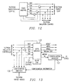
- FIGURE 12 illustrates pertinent portions of exemplary embodiments of the emulator of FIGURE 2, including the state machine which can perform the operations described above with respect to FIGURES 6-11.
- the TCK, TDI , TDO and TMS connections can be used for communication of non-scan information between the emulator and the target chip, and the state machine can suitably tri-state the TMS, TDO and TCK lines when they are used for non-scan purposes.
- FIGURE 13 diagrammatically illustrates pertinent portions of exemplary embodiments of the target device of FIGURES 2, 4 and 5.
- the scan interface adapter of the target chip includes a state machine 132 which can perform the operations described above with respect to FIGURES 6-11, along with a delay line which delays the time division multiplexed information received from the emulator appropriately to demultiplex the time division multiplexed signals. These demultiplexed signals can then be output on their respective signal lines to the cores of the target device, as shown in FIGURE 2.
- the state machine 132 can tri-state the TDO output of the target device when this connection is being used for non-scan purposes.
- FIGURE 13 also illustrates configuration switches at 135 which permit the emulator to access desired target nodes within the target device, for example, to obtain debug information.
- the signal connections for TCK, TDO, TDI and TMS can be utilized for non-scan purposes such as debug operation.
- a configuration register 137 is provided in the data scan path of the target device in order to permit the emulator to scan therein configuration information which controls the configuration of the switches 135 such that the desired nodes within the target device can be accessed.
- the state machine also includes a tri-state control line 131 which can tri-state the outputs of the configuration switch section 135 as necessary when the associated emulator connections are being used for scan purposes.
- new mode information can be sent to the target device, either on the TDI pin of the target device (for J_5 or J_4 operation) or on the TDO pin of the target device (for J_3 operation).
- the MSB will always be transmitted in the next available emulator-to-target device scan information slot, whether scanned from the emulator's TDI pin to the target device's TDO pin (for modes J_4 and J_5) or from the emulator's TDI pin to the target device's TDO pin (for J_3 operation).
- the DLY1 signal is the output of the delay line of FIGURE 13, for example a four-bit delay line needed to delay TMS values in modes J_3 and J_4 (see also FIGURES 6 and 8).
- the signal GTCK is a gated version of TCK, as produced by state machine 132 to drive signal MTCK of FIGURE 2 during the J_4 operations of FIGURES 6 and 7 and during the J_3 operations of FIGURES 8 and 9.
- a scan interface adaptor may only convert between J_3 and J_5, or between J_4 and J_5.
- the emulator can automatically detect which conversion (if any) is supported, by trying to communicate with the target device first according to J_3 protocol, then J_4 protocol, and then J_5 protocol. The target device will respond correctly only when the correct protocol is used by the emulator.
- the scan interface is actually disabled in this mode.
- the emulator expects the pins normally assigned to TCK, TMS, TDI, and TDO functions to be assigned to other functions such as debug functions.
- the state machine in the scan interface adapter is forced to state 0xF (see also FIGURES 6 and 8) while the mode is J_1.
- the assertion of TRST by the emulator causes the mode to change asynchronously from J_1 to the default mode (either J_3, J_4 or J_5), as shown in FIGURES 23-25.
- the present invention permits emulator-to-target device connections normally allocated to the scan interface to be selectively allocated to other desired functions, for example debug functions, which are thus overlaid on the usual scan interface functions. This advantageously provides more target device pins for desired non-scan communication with the emulator.
Landscapes
- Engineering & Computer Science (AREA)
- General Engineering & Computer Science (AREA)
- Theoretical Computer Science (AREA)
- Physics & Mathematics (AREA)
- General Physics & Mathematics (AREA)
- Computer Hardware Design (AREA)
- Quality & Reliability (AREA)
- Test And Diagnosis Of Digital Computers (AREA)
- Debugging And Monitoring (AREA)
- Time-Division Multiplex Systems (AREA)
Applications Claiming Priority (6)
| Application Number | Priority Date | Filing Date | Title |
|---|---|---|---|
| US515093 | 1983-07-19 | ||
| US18632600P | 2000-03-02 | 2000-03-02 | |
| US51509300A | 2000-03-02 | 2000-03-02 | |
| US21934000P | 2000-03-02 | 2000-03-02 | |
| US219340P | 2000-03-02 | ||
| US186326P | 2000-03-02 |
Publications (3)
| Publication Number | Publication Date |
|---|---|
| EP1139108A2 true EP1139108A2 (de) | 2001-10-04 |
| EP1139108A3 EP1139108A3 (de) | 2004-01-02 |
| EP1139108B1 EP1139108B1 (de) | 2006-03-22 |
Family
ID=27392080
Family Applications (4)
| Application Number | Title | Priority Date | Filing Date |
|---|---|---|---|
| EP01200792.8A Expired - Lifetime EP1139220B1 (de) | 2000-03-02 | 2001-03-02 | Erhaltung und Abgabe von Prozessoreingebauten Ablaufverfolgungs- und Taktinformationen |
| EP01200790A Expired - Lifetime EP1139108B1 (de) | 2000-03-02 | 2001-03-02 | Abtastschnittstelle mit Zeitmultiplexmerkmal zur Signalüberlagerung |
| EP01000035A Expired - Lifetime EP1130501B1 (de) | 2000-03-02 | 2001-03-02 | Dynamisch konfigurierbare Debug-Schnittstelle mit gleichzeitiger Verwendung von Fehlerbeseitigung von mehreren Prozessorkernen |
| EP01200793.6A Expired - Lifetime EP1132816B1 (de) | 2000-03-02 | 2001-03-02 | Automatische Erkennung der Verbindung zwischen einem Emulator und einem Zielgerät |
Family Applications Before (1)
| Application Number | Title | Priority Date | Filing Date |
|---|---|---|---|
| EP01200792.8A Expired - Lifetime EP1139220B1 (de) | 2000-03-02 | 2001-03-02 | Erhaltung und Abgabe von Prozessoreingebauten Ablaufverfolgungs- und Taktinformationen |
Family Applications After (2)
| Application Number | Title | Priority Date | Filing Date |
|---|---|---|---|
| EP01000035A Expired - Lifetime EP1130501B1 (de) | 2000-03-02 | 2001-03-02 | Dynamisch konfigurierbare Debug-Schnittstelle mit gleichzeitiger Verwendung von Fehlerbeseitigung von mehreren Prozessorkernen |
| EP01200793.6A Expired - Lifetime EP1132816B1 (de) | 2000-03-02 | 2001-03-02 | Automatische Erkennung der Verbindung zwischen einem Emulator und einem Zielgerät |
Country Status (2)
| Country | Link |
|---|---|
| EP (4) | EP1139220B1 (de) |
| DE (2) | DE60118089T2 (de) |
Cited By (3)
| Publication number | Priority date | Publication date | Assignee | Title |
|---|---|---|---|---|
| CN103136138A (zh) * | 2011-11-24 | 2013-06-05 | 炬力集成电路设计有限公司 | 一种芯片、芯片调试方法以及芯片与外部设备通信的方法 |
| GB2501333A (en) * | 2012-07-09 | 2013-10-23 | Ultrasoc Technologies Ltd | Controlling transportation of debug data on an integrated circuit chip |
| WO2016080969A1 (en) * | 2014-11-18 | 2016-05-26 | Hewlett Packard Enterprise Development Lp | User interface overlay |
Families Citing this family (12)
| Publication number | Priority date | Publication date | Assignee | Title |
|---|---|---|---|---|
| US7702964B2 (en) * | 2004-05-11 | 2010-04-20 | Qualcomm Incorporated | Compression of data traces for an integrated circuit with multiple memories |
| ATE367607T1 (de) * | 2005-05-02 | 2007-08-15 | Accemic Gmbh & Co Kg | Verfahren und vorrichtung zur emulation einer programmierbaren einheit |
| DE102007017865A1 (de) | 2007-04-13 | 2008-11-13 | Dspace Digital Signal Processing And Control Engineering Gmbh | Adaptions-Element und Testanordnung sowie Verfahren zum Betrieb derselben |
| US9111046B2 (en) | 2013-06-12 | 2015-08-18 | International Business Machines Corporation | Implementing capacity and user-based resource allocation for a shared adapter in a virtualized system |
| US9720775B2 (en) | 2013-06-12 | 2017-08-01 | International Business Machines Corporation | Implementing concurrent adapter firmware update for an SRIOV adapter in a virtualized system |
| US9400704B2 (en) | 2013-06-12 | 2016-07-26 | Globalfoundries Inc. | Implementing distributed debug data collection and analysis for a shared adapter in a virtualized system |
| US9323620B2 (en) | 2013-06-12 | 2016-04-26 | International Business Machines Corporation | Implementing shared adapter configuration updates concurrent with maintenance actions in a virtualized system |
| US9317317B2 (en) | 2013-06-12 | 2016-04-19 | International Business Machines Corporation | Implementing concurrent device driver maintenance and recovery for an SRIOV adapter in a virtualized system |
| US9304849B2 (en) | 2013-06-12 | 2016-04-05 | International Business Machines Corporation | Implementing enhanced error handling of a shared adapter in a virtualized system |
| US10073137B2 (en) | 2016-08-02 | 2018-09-11 | Qualcomm Incorporated | Soundwire-based embedded debugging in an electronic device |
| CN111209193B (zh) * | 2019-12-30 | 2023-09-22 | 北京水滴科技集团有限公司 | 程序的调试方法及装置 |
| CN114062896A (zh) * | 2021-11-11 | 2022-02-18 | 深圳市慧邦电子科技有限公司 | 一种集成电路的成品测试方法和存储介质 |
Citations (3)
| Publication number | Priority date | Publication date | Assignee | Title |
|---|---|---|---|---|
| GB2218816A (en) * | 1988-05-19 | 1989-11-22 | Plessey Co Plc | Testing integrated circuits |
| US5347523A (en) * | 1992-03-02 | 1994-09-13 | Motorola, Inc. | Data processing system having serial self address decoding and method of operation |
| US5943490A (en) * | 1997-05-30 | 1999-08-24 | Quickturn Design Systems, Inc. | Distributed logic analyzer for use in a hardware logic emulation system |
Family Cites Families (13)
| Publication number | Priority date | Publication date | Assignee | Title |
|---|---|---|---|---|
| US4703484A (en) * | 1985-12-19 | 1987-10-27 | Harris Corporation | Programmable integrated circuit fault detection apparatus |
| JPH01259274A (ja) * | 1988-04-08 | 1989-10-16 | Fujitsu Ltd | 集積回路の試験方式 |
| US5369645A (en) * | 1991-07-02 | 1994-11-29 | Hewlett-Packard Company | Testing integrated circuit pad input and output structures |
| US5513186A (en) * | 1993-12-07 | 1996-04-30 | Sun Microsystems, Inc. | Method and apparatus for interconnect testing without speed degradation |
| EP0720093B1 (de) * | 1994-12-28 | 2001-11-14 | Kabushiki Kaisha Toshiba | Mikroprozessor mit Fehlersuchsystem |
| US5615357A (en) * | 1994-12-29 | 1997-03-25 | Sun Microsystems, Inc. | System and method for verifying processor performance |
| US5729726A (en) * | 1995-10-02 | 1998-03-17 | International Business Machines Corporation | Method and system for performance monitoring efficiency of branch unit operation in a processing system |
| US5832490A (en) * | 1996-05-31 | 1998-11-03 | Siemens Medical Systems, Inc. | Lossless data compression technique that also facilitates signal analysis |
| US5848264A (en) * | 1996-10-25 | 1998-12-08 | S3 Incorporated | Debug and video queue for multi-processor chip |
| US6154857A (en) * | 1997-04-08 | 2000-11-28 | Advanced Micro Devices, Inc. | Microprocessor-based device incorporating a cache for capturing software performance profiling data |
| US5978902A (en) * | 1997-04-08 | 1999-11-02 | Advanced Micro Devices, Inc. | Debug interface including operating system access of a serial/parallel debug port |
| GB9805479D0 (en) | 1998-03-13 | 1998-05-13 | Sgs Thomson Microelectronics | Microcomputer |
| EP1380848B1 (de) | 1998-06-16 | 2009-09-23 | Infineon Technologies AG | Einrichtung zur Vermessung und Analyse von elektrischen Signalen eines integrierten Schaltungsbausteins |
-
2001
- 2001-03-02 EP EP01200792.8A patent/EP1139220B1/de not_active Expired - Lifetime
- 2001-03-02 EP EP01200790A patent/EP1139108B1/de not_active Expired - Lifetime
- 2001-03-02 EP EP01000035A patent/EP1130501B1/de not_active Expired - Lifetime
- 2001-03-02 DE DE60118089T patent/DE60118089T2/de not_active Expired - Lifetime
- 2001-03-02 DE DE60139219T patent/DE60139219D1/de not_active Expired - Lifetime
- 2001-03-02 EP EP01200793.6A patent/EP1132816B1/de not_active Expired - Lifetime
Patent Citations (3)
| Publication number | Priority date | Publication date | Assignee | Title |
|---|---|---|---|---|
| GB2218816A (en) * | 1988-05-19 | 1989-11-22 | Plessey Co Plc | Testing integrated circuits |
| US5347523A (en) * | 1992-03-02 | 1994-09-13 | Motorola, Inc. | Data processing system having serial self address decoding and method of operation |
| US5943490A (en) * | 1997-05-30 | 1999-08-24 | Quickturn Design Systems, Inc. | Distributed logic analyzer for use in a hardware logic emulation system |
Cited By (6)
| Publication number | Priority date | Publication date | Assignee | Title |
|---|---|---|---|---|
| CN103136138A (zh) * | 2011-11-24 | 2013-06-05 | 炬力集成电路设计有限公司 | 一种芯片、芯片调试方法以及芯片与外部设备通信的方法 |
| CN103136138B (zh) * | 2011-11-24 | 2015-07-01 | 炬力集成电路设计有限公司 | 一种芯片、芯片调试方法以及芯片与外部设备通信的方法 |
| GB2501333A (en) * | 2012-07-09 | 2013-10-23 | Ultrasoc Technologies Ltd | Controlling transportation of debug data on an integrated circuit chip |
| GB2501333B (en) * | 2012-07-09 | 2014-03-05 | Ultrasoc Technologies Ltd | Debug architecture |
| US9026871B2 (en) | 2012-07-09 | 2015-05-05 | Ultrasoc Technologies Ltd. | Prioritizing transport of debug data on an integrated circuit chip by data type |
| WO2016080969A1 (en) * | 2014-11-18 | 2016-05-26 | Hewlett Packard Enterprise Development Lp | User interface overlay |
Also Published As
| Publication number | Publication date |
|---|---|
| DE60118089T2 (de) | 2006-10-05 |
| EP1139220A2 (de) | 2001-10-04 |
| EP1130501A1 (de) | 2001-09-05 |
| EP1132816A2 (de) | 2001-09-12 |
| EP1132816B1 (de) | 2019-03-13 |
| EP1130501B1 (de) | 2009-07-15 |
| DE60139219D1 (de) | 2009-08-27 |
| EP1139108A3 (de) | 2004-01-02 |
| EP1139220A3 (de) | 2009-10-28 |
| EP1132816A3 (de) | 2005-09-07 |
| DE60118089D1 (de) | 2006-05-11 |
| EP1139108B1 (de) | 2006-03-22 |
| EP1139220B1 (de) | 2017-10-25 |
Similar Documents
| Publication | Publication Date | Title |
|---|---|---|
| US6947884B2 (en) | Scan interface with TDM feature for permitting signal overlay | |
| US20150254155A1 (en) | Maintaining Coherent Synchronization Between Data Streams on Detection of Overflow | |
| EP1139108B1 (de) | Abtastschnittstelle mit Zeitmultiplexmerkmal zur Signalüberlagerung | |
| US7457739B2 (en) | Read FIFO scheduling for multiple streams while maintaining coherency | |
| US7747901B2 (en) | Auxiliary link control commands | |
| JP2002014837A (ja) | 信号オーバーレイを許容する時分割多重化機能を備えたスキャン・インタフェース |
Legal Events
| Date | Code | Title | Description |
|---|---|---|---|
| PUAI | Public reference made under article 153(3) epc to a published international application that has entered the european phase |
Free format text: ORIGINAL CODE: 0009012 |
|
| 17P | Request for examination filed |
Effective date: 20010302 |
|
| AK | Designated contracting states |
Kind code of ref document: A2 Designated state(s): AT BE CH CY DE DK ES FI FR GB GR IE IT LI LU MC NL PT SE TR |
|
| AX | Request for extension of the european patent |
Free format text: AL;LT;LV;MK;RO;SI |
|
| PUAL | Search report despatched |
Free format text: ORIGINAL CODE: 0009013 |
|
| AK | Designated contracting states |
Kind code of ref document: A3 Designated state(s): AT BE CH CY DE DK ES FI FR GB GR IE IT LI LU MC NL PT SE TR |
|
| AX | Request for extension of the european patent |
Extension state: AL LT LV MK RO SI |
|
| 17Q | First examination report despatched |
Effective date: 20040706 |
|
| AKX | Designation fees paid |
Designated state(s): AT BE CH CY DE DK ES FI FR GB GR IE IT LI LU MC NL PT SE TR |
|
| RBV | Designated contracting states (corrected) |
Designated state(s): DE FR GB |
|
| GRAP | Despatch of communication of intention to grant a patent |
Free format text: ORIGINAL CODE: EPIDOSNIGR1 |
|
| GRAS | Grant fee paid |
Free format text: ORIGINAL CODE: EPIDOSNIGR3 |
|
| GRAA | (expected) grant |
Free format text: ORIGINAL CODE: 0009210 |
|
| AK | Designated contracting states |
Kind code of ref document: B1 Designated state(s): DE FR GB |
|
| REG | Reference to a national code |
Ref country code: GB Ref legal event code: FG4D |
|
| REF | Corresponds to: |
Ref document number: 60118089 Country of ref document: DE Date of ref document: 20060511 Kind code of ref document: P |
|
| ET | Fr: translation filed | ||
| PLBE | No opposition filed within time limit |
Free format text: ORIGINAL CODE: 0009261 |
|
| STAA | Information on the status of an ep patent application or granted ep patent |
Free format text: STATUS: NO OPPOSITION FILED WITHIN TIME LIMIT |
|
| 26N | No opposition filed |
Effective date: 20061227 |
|
| REG | Reference to a national code |
Ref country code: FR Ref legal event code: PLFP Year of fee payment: 16 |
|
| PGFP | Annual fee paid to national office [announced via postgrant information from national office to epo] |
Ref country code: FR Payment date: 20160223 Year of fee payment: 16 Ref country code: GB Payment date: 20160224 Year of fee payment: 16 |
|
| PGFP | Annual fee paid to national office [announced via postgrant information from national office to epo] |
Ref country code: DE Payment date: 20160324 Year of fee payment: 16 |
|
| REG | Reference to a national code |
Ref country code: DE Ref legal event code: R119 Ref document number: 60118089 Country of ref document: DE |
|
| GBPC | Gb: european patent ceased through non-payment of renewal fee |
Effective date: 20170302 |
|
| REG | Reference to a national code |
Ref country code: FR Ref legal event code: ST Effective date: 20171130 |
|
| PG25 | Lapsed in a contracting state [announced via postgrant information from national office to epo] |
Ref country code: DE Free format text: LAPSE BECAUSE OF NON-PAYMENT OF DUE FEES Effective date: 20171003 Ref country code: FR Free format text: LAPSE BECAUSE OF NON-PAYMENT OF DUE FEES Effective date: 20170331 |
|
| PG25 | Lapsed in a contracting state [announced via postgrant information from national office to epo] |
Ref country code: GB Free format text: LAPSE BECAUSE OF NON-PAYMENT OF DUE FEES Effective date: 20170302 |