EP1134810A2 - Feldeffekttransistor - Google Patents
Feldeffekttransistor Download PDFInfo
- Publication number
- EP1134810A2 EP1134810A2 EP00127979A EP00127979A EP1134810A2 EP 1134810 A2 EP1134810 A2 EP 1134810A2 EP 00127979 A EP00127979 A EP 00127979A EP 00127979 A EP00127979 A EP 00127979A EP 1134810 A2 EP1134810 A2 EP 1134810A2
- Authority
- EP
- European Patent Office
- Prior art keywords
- layer
- semiconductor
- film thickness
- barrier layer
- gate
- Prior art date
- Legal status (The legal status is an assumption and is not a legal conclusion. Google has not performed a legal analysis and makes no representation as to the accuracy of the status listed.)
- Withdrawn
Links
Images










Classifications
-
- H—ELECTRICITY
- H10—SEMICONDUCTOR DEVICES; ELECTRIC SOLID-STATE DEVICES NOT OTHERWISE PROVIDED FOR
- H10D—INORGANIC ELECTRIC SEMICONDUCTOR DEVICES
- H10D30/00—Field-effect transistors [FET]
- H10D30/40—FETs having zero-dimensional [0D], one-dimensional [1D] or two-dimensional [2D] charge carrier gas channels
- H10D30/47—FETs having zero-dimensional [0D], one-dimensional [1D] or two-dimensional [2D] charge carrier gas channels having two-dimensional [2D] charge carrier gas channels, e.g. nanoribbon FETs or high electron mobility transistors [HEMT]
-
- H—ELECTRICITY
- H10—SEMICONDUCTOR DEVICES; ELECTRIC SOLID-STATE DEVICES NOT OTHERWISE PROVIDED FOR
- H10D—INORGANIC ELECTRIC SEMICONDUCTOR DEVICES
- H10D30/00—Field-effect transistors [FET]
- H10D30/40—FETs having zero-dimensional [0D], one-dimensional [1D] or two-dimensional [2D] charge carrier gas channels
- H10D30/47—FETs having zero-dimensional [0D], one-dimensional [1D] or two-dimensional [2D] charge carrier gas channels having two-dimensional [2D] charge carrier gas channels, e.g. nanoribbon FETs or high electron mobility transistors [HEMT]
- H10D30/471—High electron mobility transistors [HEMT] or high hole mobility transistors [HHMT]
- H10D30/473—High electron mobility transistors [HEMT] or high hole mobility transistors [HHMT] having confinement of carriers by multiple heterojunctions, e.g. quantum well HEMT
Definitions
- the present invention relates to a field effect transistor (abbreviated to "FET” in this specification), and more specifically to a heterojunction FET having a large gate forward direction rising voltage.
- FET field effect transistor
- a GaAs FET is used as a high power output element in a transmitter of a mobile communication terminal, since the GaAs FET has a low on-resistance and can operate at a low voltage with a high efficiency.
- a high power GaAs FET is demanded not only to be an enhancement type having a positive threshold voltage but also to have a feature that a leak drain current at a gate voltage of 0V is perfectly cut off. If this demand is satisfied, it becomes possible to omit a DC/DC converter for generating a negative voltage for a gate bias and a drain bias switch for cutting off the drain current, which were required in the prior art, with the result that a mobile terminal can further be reduced in size and in weight.
- an enhancement type FET having a threshold voltage of not less than for example 0.3V will be exemplified.
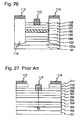
- Fig. 27 there is shown a diagrammatic sectional view of an example of an enhancement type heterojunction FET having a threshold voltage of 0.3V.
- the enhancement type heterojunction GaAs FET includes an undoped Al 0.2 Ga 0.8 As gate contact layer 708 having a low aluminum composition ratio in order to avoid a problem of a surface oxidation, and an Si-doped Al 0.2 Ga 0.8 As electron supplying layer 707, an undoped Al 0.2 Ga 0.8 As spacer layer 706 and an undoped In 0.2 Ga 0.8 As channel layer 705, which have a low aluminum composition ratio in order to avoid a problem of a DX center.
- the reference number 701 designates a semi-insulative GaAs substrate, and the reference number 702 indicates an undoped Al 0.2 Ga 0.8 As buffer layer.
- the reference number 703 shows a Si-doped A1 0.2 Ga 0.8 As electron supplying layer, and the reference number 704 denotes an undoped Al 0.2 Ga 0.8 As spacer layer.
- the reference number 709 designates an undoped GaAs gate buried layer, and the reference number 710 indicates an Si-doped Al 0.2 Ga 0.8 As wide recess stopper layer.
- the reference number 711 shows an Si-doped GaAs cap layer, and the reference number 712 denotes a gate electrode.
- the reference number 713 designates a source electrode, and the reference number 714 designates a drain electrode.
- a gate forward direction voltage is 0.7V.
- a switching width of a gate voltage becomes small.
- JP-A-09-246525 proposes an enhancement type FET having a gate forward direction voltage elevated by using a barrier layer formed of an AlGaAs semiconductor layer having a high aluminum composition ratio.
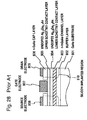
- Fig. 28 there is shown a diagrammatic sectional view of an example disclosed in JP-A-09-246525, in which a gate forward direction voltage is elevated to 1.5V by using a barrier layer 804 formed of an Al 0.8 Ga 0.2 As semiconductor layer (undoped AlGaAs lower Schottky contact layer) having a thickness of 20nm.
- the reference number 801 designates a scmi-insulative GaAs substrate, and the reference number 802 indicates a buffer layer.
- the reference number 803 shows a Si-doped InGaAs channel layer, and the reference number 805 denotes an undoped Al 0.3 Ga 0.7 As upper Schottky contact layer.
- the reference number 806 designates an Si-doped GaAs cap layer, and the reference number 807 indicates a gate electrode.
- the reference number 808 shows a source electrode, and the reference number 809 denotes a drain electrode.
- the reference number designates a silicon implanted region.
- this second example includes a thick barrier layer exists between a channel layer and each of a source electrode and a drain electrode, so that a similar problem is encountered in which it is necessary to reduce a contact resistance by use of an Si-ion implantation process.
- this second example has a single doped epitaxial structure in which an electron supplying layer is provided only under an undoped channel layer. Since no impurity is doped in the channel layer, the mobility in the channel layer is high. However, because of the single doped structure in which the electron supplying layer is provided only under the channel layer, a sheet carrier concentration in the channel is low, with the result that a drain current is as small as 180 - 200 mA/mm
- JP-A-59-028383 proposes a heterojunction FET structure in which a potential barrier is provided just above the channel to prevent high energy electrons in the channel layer from being scattered into an electron supplying layer. Since this proposed structure has an AlGaAs layer having a high aluminum composition ratio provided on the channel layer, it is effective in elevating the gate forward direction voltage.
- a thick barrier layer is formed of an AlAs layer having a thickness of 40 ⁇ and an Al 0.55 Ga 0.45 As layer having a thickness of 500 ⁇ , the contact resistance is large and a maximum drain current is small.
- Another object of the present invention is to provide a field effect transistor which has a large maximum drain current or a low on-resistance and which can be fabricated without increasing a complicated fabricating step exemplified by an ion implantation.
- Still another object of the present invention is to provide a field effect transistor of an epitaxial structure which has a reduced gate leak current in a gate forward direction biasing condition, so that a gate forward direction rising voltage can be elevated.
- a field effect transistor which includes at least a first semiconductor layer in which carriers flows, and a second semiconductor layer formed on the first semiconductor layer, the second semiconductor layer having an electron affinity smaller that of the first semiconductor layer, and the second semiconductor layer being doped with an n-type impurity, wherein a semiconductor barrier layer is inserted between the first semiconductor layer and the second semiconductor layer, the semiconductor barrier layer having a positive electron energy at a conduction band bottom of a ⁇ valley, in comparison with an electron energy at a conduction band bottom of a ⁇ valley in the second semiconductor layer, the semiconductor barrier layer having a film thickness of not less than 3nm but not greater than 10nm.
- the semiconductor barrier layer When the semiconductor barrier layer is in lattice mismatching with a semiconductor substrate on which semiconductor layers are grown, and if a maximum film thickness of the semiconductor barrier layer in which no dislocation occurs, is less than 10nm, the semiconductor barrier layer has the film thickness of not less than 3nm but not greater than the maximum film thickness in which no dislocation occurs.
- the first semiconductor layer is formed of a material selected from the group consisting of InGaAs and GaAs
- the second semiconductor layer is formed of a material selected from the group consisting of Al X 1 Ga 1-X 1 As where 0 ⁇ X 1 ⁇ 0.3
- InGaP and the semiconductor barrier layer is formed of Al X 2 Ga 1-X 2 As where 0.4 ⁇ X 2 ⁇ 1.
- the first semiconductor layer is formed of a material selected from the group consisting of InGaAs and GaAs
- the second semiconductor layer is formed of a material selected from the group consisting of Al X 1 Ga 1-X 1 As where 0 ⁇ X 1 ⁇ 0.3, and InGaP
- the semiconductor barrier layer is formed of (Al X 2 Ga 1-X 2 ) Y In 1-Y P where 0.2 ⁇ X 2 ⁇ 1, and 0.4 ⁇ Y ⁇ 0.6.
- the first semiconductor layer is formed of a material selected from the group consisting of InGaAs and GaAs
- the second semiconductor layer is formed of a material selected from the group consisting of Al X 1 Ga 1-X 1 As where 0 ⁇ X 1 ⁇ 0.3, and InGaP
- the semiconductor barrier layer is formed of (Al X 2 Ga 1-X 2 ) Y In 1-Y P where 0 ⁇ X 2 ⁇ 1, and 0.6 ⁇ Y ⁇ 1.
- the first semiconductor layer is formed of InGaAs
- the second semiconductor layer is formed of a material selected from the group consisting of AlInAs and AlGaInAs
- the semiconductor barrier layer is formed of (Al X Ga 1-X ) Y In 1-Y As where 0.4 ⁇ X ⁇ 1, and 0.6 ⁇ Y ⁇ 1.
- the semiconductor barrier layer having an undoped layer portion near to a channel layer and an n-type impurity doped layer portion at a gate electrode side.
- the semiconductor barrier layer is formed of a material selected from the group consisting of (Al X Ga 1-X ) Y In 1-Y P where 0.2 ⁇ X ⁇ 0.3, and 0.4 ⁇ Y ⁇ 1.0 and (Al X Ga 1- X ) Y In 1-Y As where 0.4 ⁇ X ⁇ 1, and 0.6 ⁇ Y ⁇ 0.7, and the semiconductor barrier layer having an undoped layer portion at a side of the first semiconductor layer and an n-type impurity doped layer portion at a gate electrode side.
- the field effect transistor in accordance with the first aspect of the present invention can further includes an n-type impurity doped semiconductor layer formed under the first semiconductor layer and having an electron affinity smaller that of the first semiconductor layer.
- a field effect transistor which includes at least a first semiconductor layer in which carriers flows, and a second semiconductor layer formed on the first semiconductor layer, the second semiconductor layer having an electron affinity smaller that of the first semiconductor layer, and the second semiconductor layer being doped with an n-type impurity, wherein a first semiconductor barrier layer is inserted between the first semiconductor layer and the second semiconductor layer, and a second semiconductor barrier layer is inserted between the second semiconductor layer and a gate electrode, each of the first and second semiconductor barrier layers having a positive electron energy at a conduction band bottom of a ⁇ valley, in comparison with an electron energy at a conduction band bottom of a ⁇ valley in the second semiconductor layer, each of the first and second semiconductor barrier layers having a film thickness of not less than 3nm but not greater than 10nm.
- the at least one of the first and second semiconductor barrier layers When at least one of the first and second semiconductor barrier layers is in lattice mismatching with a semiconductor substrate on which semiconductor layers are grown, if a maximum film thickness of the at least one of the first and second semiconductor barrier layers in which no dislocation occurs, is less than 10nm, the at least one of the first and second semiconductor barrier layers has the film thickness of not less than 3nm but not greater than the maximum film thickness in which no dislocation occurs.
- the first semiconductor layer is formed of a material selected from the group consisting of InGaAs and GaAs
- the second semiconductor layer is formed of a material selected from the group consisting of Al X 1 Ga 1-X 1 As where 0 ⁇ X 1 ⁇ 0.3, and InGaP.
- the first semiconductor barrier layer is formed of a material selected from the group consisting of Al X 2 Ga 1-X 2 AS where 0.4 ⁇ X 2 ⁇ 1, (Al X 3 Ga 1-X 3 ) Y1 In 1-Y1 P where 0.2 ⁇ X 3 ⁇ 1, and 0.4 ⁇ Y 1 ⁇ 0.6, and (Al X 4 Ga 1-X 4 ) Y2 In 1-Y2 P where 0 ⁇ X 4 ⁇ 1, and 0.6 ⁇ Y 2 ⁇ 1, and the second semiconductor barrier layer is formed of a material selected from the group consisting of Al X 5 Ga 1-X 5 As where 0.4 ⁇ X 5 ⁇ 1, (Al X 6 Ga 1-X 6 ) Y3 In 1- Y3 P where 0.2 ⁇ X 6 ⁇ 1, and 0.4 ⁇ Y 3 ⁇ 0.6, and (Al X 7 Ga 1-X 7 ) Y4 In 1-Y4 P where 0 ⁇ X 7 ⁇ 1, and 0.6 ⁇ Y 4 ⁇ 1.
- the first semiconductor layer is formed of InGaAs
- the second semiconductor layer is formed of a material selected from the group consisting of AlInAs and AlGaInAs.
- the first semiconductor barrier layer is formed of (Al X 1 Ga 1-X 1 ) Y In 1- Y1 As where 0.4 ⁇ X 1 ⁇ 1, and 0.6 ⁇ Y 1 ⁇ 1
- the second semiconductor barrier layer is formed of (Al X 2 Ga 1-X 2 ) Y 2 In 1-Y2 As where 0.4 ⁇ X 2 ⁇ 1, and 0.6 ⁇ Y 2 ⁇ 1.
- a portion or all of the first semiconductor barrier layer near to a channel layer is doped with an n-type impurity.
- the first semiconductor barrier layer near to the first semiconductor layer is formed of a material selected from the group consisting of (Al X Ga 1-X ) Y In 1-Y P where 0.2 ⁇ X ⁇ 0.3, and 0.4 ⁇ Y ⁇ 1.0 and (Al X Ga 1-X ) Y In 1-Y As where 0.4 ⁇ X ⁇ 1, and 0.6 ⁇ Y ⁇ 0.7, and a portion or all of the first semiconductor barrier layer is doped with an n-type impurity.
- the field effect transistor in accordance with the second aspect of the present invention can further include an n-type impurity doped semiconductor layer formed under the first semiconductor layer and having an electron affinity smaller that of the first semiconductor layer.
- a potential barrier formed by a semiconductor barrier layer inserted between a channel layer and an upper electron supplying layer effectively functions as a barrier in a forward direction gate biasing condition, so that a gate leak current is reduced in the forward direction gate biasing condition and a gate forward direction rising voltage can be elevated.
- a semiconductor barrier layer inserted between a channel layer and an upper electron supplying layer not only a semiconductor barrier layer inserted between a channel layer and an upper electron supplying layer, but also a semiconductor barrier layer inserted between the upper electron supplying layer and a gate electrode.
- the film thickness of the semiconductor barrier layer is not less than 3nm but not greater than 10nm, or alternatively, not less than 3nm but not greater than the maximum film thickness in which no dislocation occurs.
- a channel layer side portion of the semiconductor barrier layer is not doped with impurity, but a gate electrode side portion of the semiconductor barrier layer is doped with an n-type impurity, so that a portion of the semiconductor barrier layer functions as an electron supplying layer.
- a very large number of electrons are accumulated in the channel layer, so that a maximum drain current can be further increased.
- a portion or all of the semiconductor barrier layer near to a channel layer is doped with an n-type impurity.
- a very large number of clcctrons are accumulated in the channel layer, so that a maximum drain current can be further increased.
- a diagrammatic sectional view of a heterojunction FET which is a first embodiment of the FET in accordance with the present invention.
- the reference number 101 designates a semi-insulative GaAs substrate, and the reference number 102 indicates an undoped Al 0.2 Ga 0.8 As buffer layer.
- the reference number 103 shows a Si-doped Al 0.2 Ga 0.8 As lower electron supplying layer, and the reference number 104 denotes an undoped Al 0.2 Ga 0.8 As spacer layer.
- the reference number 105 designates an undoped In 0.2 Ga 0.8 As channel layer, and the reference number 106 indicates an undoped Al 0.5 Ga 0.5 As barrier layer.
- the reference number 107 shows an Si-doped Al 0.2 Ga 0.8 As upper electron supplying layer, and the reference number 108 denotes an undoped Al 0.2 Ga 0.8 As gate contact layer.
- the reference number 109 designates an undoped GaAs gate buried layer, and the reference number 110 indicates an Si-doped Al 0.2 Ga 0.8 As wide recess stopper layer.
- the reference number 111 shows an Si-doped GaAs cap layer, and the reference number 112 denotes a gate electrode.
- the reference number 113 designates a source electrode, and the reference number 114 designates a drain electrode.
- the field effect transistor in this embodiment is characterized in that the undoped Al 0.5 Ga 0.5 As barrier layer 106 having a film thickness of 5nm is formed between the undoped In 0.2 Ga 0.8 As channel layer 105 and the Si-doped Al 0.2 Ga 0.8 As upper electron supplying layer 107.
- the undoped Al 0.5 Ga 0.5 As barrier layer 106 forms a barrier layer which is higher than that in the prior art using the undoped Al 0.2 Ga 0.8 As spacer layer 706 shown in Fig. 27, by 0.2eV in the r valley
- Fig. 2 illustrates a conduction band profile in the X1-Y1 direction in Fig. 1 when various voltages "Vg" of +0.3V, +0.8V and +1.3V are applied to the gate electrode 112.
- Vg voltages
- a potential barrier is formed just above the channel. If a gate bias voltage "Vg" is gradually increased in a forward direction, the height of the Schottky barrier formed by a contact with the gate electrode gradually becomes low, but the height of the potential barrier formed just above the channel does not substantially change, so that the potential barrier formed just above the channel effectively functions as a barrier against electrons within the channel.
- Vg gate bias voltage
- Fig. 3 illustrates a gate voltage dependency of the gate forward direction current.
- the gate voltage is less than 0.3V
- the structure of Fig. 1 and the prior art structure have a gate current of substantially the same magnitude.
- the gate voltage is not less than 0.3V
- the barrier layer formed just above the channel layer starts to exert its function, so that the gate current is suppressed in the structure of Fig. 1.
- the gate forward direction rising voltage which is defined to be a gate voltage when a gate current is at 1mA/mm, can be elevated.
- Figs. 4A and 4B illustrates a dependency to the film thickness of the barrier layer 106, of a sheet carrier concentration accumulated in the channel layer, an on-resistance, and the gate forward direction rising voltage.
- the barrier layer 106 has the film thickness of 3nm.
- the film thickness of the barrier layer 106 becomes large, the distance between the Al 0.2 Ga 0.8 As upper electron supplying layer 107 and the undoped In 0.2 Ga 0.8 As channel layer 105 becomes large, so that the carrier concentration accumulated in the channel layer lowers.
- the film thickness of the barrier layer 106 becomes large, the contact resistance between the channel layer and each of the source electrode and the drain electrode becomes large, so that the on-resistance in the FET becomes large.
- the film thickness of the barrier layer 106 exceeds 10nm, the on-resistance abruptly increases. Therefore, in order to avoid an increase of a parasite resistance component (on-resistance), it is sufficient if the film thickness of the barrier layer 106 is not greater than 10nm.
- the heterojunction FET of the first embodiment as mentioned above has a threshold voltage of +0.3V and the gate forward direction rising voltage of +1.1V. This gate forward direction rising voltage becomes higher than that of the prior art heterojunction FET by 0.4V.
- the heterojunction FET of the first embodiment since the heterojunction FET of the first embodiment has a double doped structure in which the electron supplying layers are formed above and under the channel layer, respectively, a maximum drain current is as large as 350mA/mm.
- Figs. 5A to 5F are diagrammatic sectional views illustrating a process for fabricating the heterojunction FET shown in Fig. 1.
- an undoped Al 0.2 Ga 0.8 As buffer layer 102 having a film thickness of 500nm
- an Al 0.2 Ga 0.8 As electron supplying layer 103 doped with Si at an impurity concentration of 4 ⁇ 10 18 cm -3 and having a film thickness of 4nm
- an undoped Al 0.2 Ga 0.8 As spacer layer 104 having a film thickness of 2nm
- an undoped In 0.2 Ga 0.8 As channel layer 105 having a film thickness of 15nm
- an undoped Al 0.5 Ga 0.5 As barrier layer 106 having a film thickness of 5nm
- an Al 0.2 Ga 0.8 As electron supplying layer 107 doped with Si at an impurity concentration of 4 ⁇ 10 18 cm -3 and having a film thickness of 9nm
- a patterned mask 115 having an opening corresponding to a wide recess is formed on the GaAs cap layer 111 of the substrate thus formed.
- the GaAs cap layer 111 is selectively etched by using the patterned mask 115 as an etching mask and by using the Al 0.2 Ga 0.8 As wide recess stopper layer 110 as an etching stopper layer.
- the Al 0.2 Ga 0.8 As wide recess stopper layer 110 is selectively etched by using the patterned mask 115 as an etching mask.
- a new mask 116 having an opening corresponding to a gate recess is formed as shown in Fig. 5C.
- the GaAs gate buried layer 109 is selectively etched by using the patterned mask 116 as an etching mask and by using the Al 0.2 Ga 0.8 As gate contact layer 108 as an etching stopper layer, as shown in Fig. 5D.
- a WSi gate electrode 112 is formed on an exposed surface of the Al 0.2 Ga 0.8 As gate contact layer 108, and the mask 116 is removed as shown in Fig. 5E. Thereafter, a not shown mask is formed for formation of the source electrode and the drain electrode, and an AuGe film is vaporized, and a lift-off process is carried out, and then, a heat treatment is performed for alloying, so that the source electrode 113 and the drain electrode 114 are formed as shown in Fig. 5F.
- the barrier layer is constituted of the AlGaAs layer having the aluminum composition ratio of 0.5 and the film thickness of 5nm.
- the film thickness is not less than 3nm but not greater than lOnm and if the aluminum composition ratio is not less than 0.4, it is possible to elevate the gate forward direction rising voltage without deteriorating the maximum drain current and the on-resistance.
- Fig. 6 is a diagrammatic sectional view of a modification of the first embodiment of the FET in accordance with the present invention.
- the heterojunction FET shown in Fig. 6 is characterized in that no gate recess is formed in the undoped GaAs gate buried layer 109 having the film thickness of 15nm shown in Fig. 1, and a GaAs layer 121 doped with a p-type impurity at an impurity concentration of 4 ⁇ 10 19 cm -3 and having a film thickness of 50nm is formed on the undoped GaAs gate buried layer 109, and the WSi gate electrode 112 is formed on the GaAs layer 121
- Fig. 7 is a potential energy diagram along the line X2-Y2 in Fig. 6 when the voltage of +0.3V is applied to the WSi gate electrode 112. Since the GaAs layer 121 doped with the p-type impurity at a high impurity concentration is used as a portion of the gate electrode, the height of the potential barrier against the electrons can be further elevated.
- the potential barrier at a gate electrode side in the heterojunction FET shown in Fig. 6 is higher than that in the heterojunction FET shown in Fig. 1 by 0.4eV.
- the heterojunction FET of this modification has the threshold voltage of 0.3V, the gate forward direction rising voltage of 1.5V, and the maximum drain current of 350mA/mm.
- the gate forward direction rising voltage is further elevated.
- the gate forward direction rising voltage becomes higher than that of the heterojunction FET shown in Fig. 1 by 0.4V.
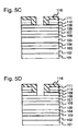
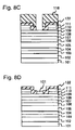
- Figs. 8A to 8F are diagrammatic sectional views illustrating a process for fabricating the heterojunction FET shown in Fig. 6.
- a patterned mask 115 having an opening corresponding to a wide recess is formed on the GaAs cap layer 111 of the substrate thus formed.
- the GaAs cap layer 111 is selectively etched by using the patterned mask 115 as an etching mask to form a wide recess, and the Al 0.2 Ga 0.8 As wide recess stopper layer 110 is selectively etched.
- an SiO 2 film 122 is formed on the whole surface. Then, a new mask 116 having an opening corresponding to a gate is formed on SiO 2 film 122 as shown in Fig. 8C.
- the SiO 2 film 122 is selectively removed by using the mask 116.
- a GaAs layer 121 doped with a p-type impurity at an impurity concentration of 4 ⁇ 10 19 cm -3 and having a film thickness of 50nm is selectively grown in an opening formed in the SiO 2 film 122 by means of the organometallic vapor phase epitaxy, as shown in Fig. 8D.
- a WSi gate electrode 112 is formed on the selectively grown GaAs layer 121, as shown in Fig. 8E. Thereafter, an AuGe film is vaporized and lifted off, and then, a heat treatment is performed for alloying, so that the source electrode 113 and the drain electrode 114 are formed as shown in Fig. 8F.
- Fig. 9 is a diagrammatic sectional view of another modification of the first embodiment of the FET in accordance with the present invention.
- the shown modification of the heterojunction FET is characterized in that the upper and lower Al 0.2 Ga 0.8 As electron supplying layers 107 and 103 are replaced with In 0.5 Ga 0.5 P electron supplying layers 107a and 103a, respectively, the AlGaAs spacer layer 104 under the channel layer is replaced with an In 0.5 Ga 0.5 P spacer layer 104a, and the AlGaAs gate contact layer 108 is replaced with an In 0.5 Ga 0.5 P gate contact layer 108a.
- This modification of the heterojunction FET has the threshold voltage of +0.3V, the gate forward direction rising voltage of +1.1V.
- the maximum drain current is as large as 350mA/mm.
- a gate-drain reverse-direction breakdown voltage is increased by 3V in comparison with heterojunction FET shown in Fig. 1.
- An impact ionization percent in the InGaP layer is lower than that in the AlGaAs layer. Therefore, by forming the electron supplying layer of the InGaP layer, it is possible to suppress the impact ionization occurring within the electron supplying layer under a high electric field generated when a gate-drain reverse-direction bias is applied, so that a reverse-direction gate current is reduced. Accordingly, a large gate-drain breakdown voltage can be obtained.
- Fig. 10 is a diagrammatic sectional view of still another modification of the first embodiment of the FET in accordance with the present invention.
- This modification of the heterojunction FET is characterized in that an undoped (Al 0.5 Ga 0.5 ) 0.5 In 0.5 P barrier layer 206 having a film thickness of 5nm is formed between an undoped In 0.2 Ga 0.8 As channel layer 205 and an In 0.5 Ga 0.5 P upper electron supplying layer 207.
- a barrier layer is formed which is higher than that in the prior art using the Al 0.2 Ga 0.8 As spacer layer, by 0.15eV in the ⁇ valley.
- This modification of the heterojunction FET has the threshold voltage of +0.3V.
- the gate forward direction rising voltage is +1.0V, and the maximum drain current is as large as 350mA/mm.
- an undoped Al 0.2 Ga 0.8 As buffer layer 202 having a film thickness of 500nm
- an In 0.5 Ga 0.5 P electron supplying layer 203 doped with Si at an impurity concentration of 4 ⁇ 10 18 cm -3 and having a film thickness of 4nm
- an undoped In 0.5 Ga 0.5 P layer 204 having a film thickness of 2nm
- an undoped In 0.2 Ga 0.8 As channel layer 205 having a film thickness of 15nm
- an undoped (Al 0.5 Ga 0.5 ) 0.5 In 0.5 P barrier layer 206 having a film thickness of 5nm
- an In 0.5 Ga 0.5 P electron supplying layer 207 doped with Si at an impurity concentration of 4 ⁇ 10 18 cm -3 and having a film thickness of 9nm
- the film thickness is not less than 3nm but not greater than 10nm, and if the condition of 0.2 ⁇ X ⁇ 1 and 0.4 ⁇ Y ⁇ 0.6 is satisfied, it is possible to elevate the gate forward direction rising voltage without deteriorating the maximum drain current and the on-resistance.
- the upper and lower electron supplying layers, the spacer layer under the channel layer and the gate contact layer are constituted of the InGaP layer, but can be constituted of an AlGaAs layer.
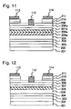
- Fig. 11 is a diagrammatic sectional view of a further modification of the first embodiment of the FET in accordance with the present invention.
- This modification of the heterojunction FET is characterized in that the undoped (Al 0.5 Ga 0.5 ) 0.5 In 0.5 P barrier layer 206 having the film thickness of 5nm, shown in Fig.
- a stacked barrier layer constituted of an undoped (Al 0.5 Ga 0.5 ) 0.5 In 0.5 P barrier layer 206a having a film thickness of 2nm, and an (Al 0.3 Ga 0.7 ) 0.5 In 0.5 P barrier layer 206b formed on the barrier layer 206a and doped with Si at an impurity concentration of 4 ⁇ 10 18 cm -3 and having a film thickness of 3nm.
- This modification of the heterojunction FET has the threshold voltage of +0.3V.
- the gate forward direction rising voltage is +1.0V, and the maximum drain current is as large as 350mA/mm.
- An epitaxially stacked structure of this modification of the heterojunction FET shown in Fig. 11 can be formed by epitaxially growing in the named order, on the semi-insulative GaAs substrate 201, by means of an organometallic vapor phase epitaxy, an undoped Al 0.2 Ga 0.8 As buffer layer 202 having a film thickness of 500nm, an In 0.5 Ga 0.5 P electron supplying layer 203 doped with Si at an impurity concentration of 4 ⁇ 10 18 cm -3 and having a film thickness of 4nm, an undoped In 0.5 Ga 0.5 P layer 204 having a film thickness of 2nm, an undoped In 0.2 Ga 0.8 As channel layer 205 having a film thickness of 15nm, an undoped (Al 0.5 Ga 0.5 ) 0.5 In 0.5 P barrier layer 206 having a film thickness of 2nm, an (Al 0.3 Ga 0.7 ) 0.5 In 0.5 P barrier layer 206b doped with Si at an impurity concentration of 4 ⁇ 10 18
- the n-type impurity doped layer is constituted of an (Al X Ga 1-X ) 0.5 In 0.5 P layer where 0.2 ⁇ X ⁇ 0.3, which does not cause the problem of the DX center.
- the semiconductor barrier layer is formed of an (Al X Ga 1-X ) Y In 1-Y P layer where 0.2 ⁇ X ⁇ 0.3 and 0.4 ⁇ Y ⁇ 1.0 (X is not greater than 0.3) or an (Al X Ga 1-X ) Y In 1-Y P layer where 0.4 ⁇ X ⁇ 1 and 0.6 ⁇ Y ⁇ 0.7 (the aluminum composition ratio XY is less than 0.7), since the problem of the DX center does not occur, it is possible to dope impurity into the barrier layer.
- the upper and lower electron supplying layers, the spacer layer under the channel layer and the gate contact layer are constituted of the InGaP layer, but can be constituted of an AlGaAs layer.
- Fig. 12 is a diagrammatic sectional view of a still further modification of the first embodiment of the FET in accordance with the present invention.
- This modification of the heterojunction FET is characterized in that an undoped (Al 0.5 Ga 0.5 ) 0.7 In 0.3 P barrier layer 306 having a film thickness of 5nm is formed between an undoped In 0.2 Ga 0.8 As channel layer 305 and an In 0.5 Ga 0.5 P upper electron supplying layer 307.
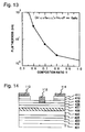
- Fig. 13 illustrates a dependency to the composition ratio Y of the critical film thickness of the (Al 0.5 Ga 0.5 ) Y In 1-Y P film grown on a GaAs substrate.
- the harrier layer is constituted of the undoped (Al 0.5 Ga 0.5 ) 0.7 In 0.3 P layer having the film thickness of 5nm.
- a barrier layer is formed which is higher than that in the prior art using the Al 0.2 Ga 0.8 As spacer layer, by 0.3eV in the ⁇ valley.
- This modification of the heterojunction FET has the threshold voltage of +0.3V.
- the gate forward direction rising voltage is +1.2V, which is higher than that in the prior art heterojunction FET by 0.5V, and the maximum drain current is as large as 350mA/mm.
- an epitaxially stacked structure of the heterojunction FET shown in Fig. 12 can be formed by epitaxially growing in the named order, on the semi-insulative GaAs substrate 301, by means of an organometallic vapor phase epitaxy, an undoped Al 0.2 Ga 0.8 As buffer layer 302 having a film thickness of 500nm, an In 0.5 Ga 0.5 P electron supplying layer 303 doped with Si at an impurity concentration of 4 ⁇ 10 18 cm -3 and having a film thickness of 4nm, an undoped In 0.5 Ga 0.5 P layer 304 having a film thickness of 2nm, an undoped In 0.2 Ga 0.8 As channel layer 305 having a film thickness of 15nm, an undoped (Al 0.5 Ga 0.5 ) 0.7 In 0.3 P barrier layer 306 having a film thickness of 5nm, an In 0.5 Ga 0.5 P electron supplying layer 307 doped with Si at an impur
- the film thickness is not less than 3nm but not greater than the critical film thickness and if the condition of 0 ⁇ X ⁇ 1 and 0.4 ⁇ Y ⁇ 0.8 is satisfied, it is possible to elevate the gate forward direction rising voltage without deteriorating the maximum drain current and the on-resistance.
- Y>0.8 the critical film thickness becomes less than 3nm, it is not longer suitable as a barrier layer.
- the upper and lower electron supplying layers, the spacer layer under the channel layer and the gate contact layer are constituted of the InGaP layer, but can be constituted of an AlGaAs layer.
- Fig. 14 is a diagrammatic sectional view of a further modification of the first embodiment of the FET in accordance with the present invention.
- This modification of the heterojunction FET is characterized in that the substrate is constituted of an InP substrate, and an undoped Al 0.7 In 0.3 As barrier layer 406 having a film thickness of 5nm is formed between an undoped In 0.53 Ga 0.47 As channel layer 405 and an Al 0.48 In 0.52 As upper electron supplying layer 407.
- Fig. 15 illustrates a dependency to a composition ratio X of a critical film thickness of the Al X In 1-X As film grown on the InP substrate.
- a high quality Al X In 1-X As layer where 0.5 ⁇ X, having no dislocation, can be obtained if the film thickness is not greater than the critical film thickness.
- the critical film thickness is 14nm.
- the barrier layer is constituted of the Al 0.7 In 0.3 As layer having the film thickness of 5nm.
- a barrier layer is formed which is higher than that in the prior art using the Al 0.2 Ga 0.8 As spacer layer, by 0.3eV in the ⁇ valley.
- This modification of the heterojunction FET has the threshold voltage of +0.3V.
- the gate forward direction rising voltage is +1.2V, which is higher than that in the prior art heterojunction FET by 0.5V, and the maximum drain current is as large as 450mA/mm.
- an epitaxially stacked structure of the heterojunction FET shown in Fig. 14 can be formed by epitaxially growing in the named order, on the semi-insulative InP substrate 401, by means of a molecular beam epitaxy or an organometallic vapor phase epitaxy, an undoped Al 0.48 In 0.52 As buffer layer 402 having a film thickness of 500nm, an Al 0.4 In 0.52 As electron supplying layer 403 doped with Si at an impurity concentration of 4 ⁇ 10 18 cm -3 and having a film thickness of 2nm, an undoped Al 0.48 In 0.52 As layer 404 having a film thickness of 2nm, an undoped In 0.53 Ga 0.47 As channel layer 405 having a film thickness of 15nm, an undoped Al 0.7 In 0.3 As barrier layer 406 having a film thickness of 5nm, an Al 0.48 In 0.52 As electron supplying layer 407 doped with Si at an impur
- the film thickness is not less than 3nm but not greater than the critical film thickness and if the condition of 0.4 ⁇ X ⁇ 1 and 0.6 ⁇ Y ⁇ 1 is satisfied, it is possible to elevate the gate forward direction rising voltage without deteriorating the maximum drain current and the on-resistance.
- the semiconductor barrier layer is formed of an (Al X Ga 1-X ) Y In 1-Y As layer where 0.4 ⁇ X ⁇ 1 and 0.6 ⁇ Y ⁇ 0.7, since the problem of the DX center does not occur, it is possible to dope impurity into the barrier layer, so that the sheet carrier concentration in the channel layer can be elevated.
- an AlInAs/InGaAs multilayer structure are epitaxially grown on the InP substrate.
- the gate forward direction rising voltage can be elevated by providing the barrier layer in a heterojunction FET including an AlGaInAs/InGaAs multilayer structure epitaxially grown on an InP substrate, and a hcterojunction FET including an AlInAs/InGaAs multilayer structure epitaxially grown on a buffer layer which is formed on a GaAs substrate for relaxing a lattice mismatching.
- FIG. 16 there is shown a diagrammatic sectional view of a heterojunction FET which is a second embodiment of the FET in accordance with the present invention.
- This second embodiment of the heterojunction FET is characterized by having a double barrier structure in which an undoped Al 0.5 Ga 0.5 As barrier layer 506 having a film thickness of 4nm is formed between an undoped In 0.2 Ga 0.8 As channel layer 505 and an Si-doped Al 0.2 Ga 0.8 As upper electron supplying layer 507, and an undoped Al 0.5 Ga 0.5 As barrier layer 508 having a film thickness of 4nm is formed between the Si-doped Al 0.2 Ga 0.8 As upper electron supplying layer 507 and an undoped Al 0.2 Ga 0.8 As gate contact layer 509.
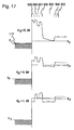
- Fig. 17 illustrates a conduction band profile in the X3-Y3 direction in Fig. 16 when various voltages "Vg" of +0.3V, +0.8V and +1.3V are applied to the gate electrode 112. If a gate bias voltage "Vg” is not greater than 0.3V, a potential barrier formed near to the gate effectively functions, and if the gate bias voltage "Vg” is increased to exceed 0.3V, the height of the potential barrier formed near to the gate becomes low, but a potential barrier formed just above the channel does not lower, with the result that the potential barrier formed just above the channel effectively functions
- Fig. 18 illustrates a gate voltage dependency of the gate forward direction current.
- this embodiment of the heterojunction FET has a threshold voltage of +0.3V, and the gate forward direction rising voltage is +1.2V.
- the gate current is reduced over a wide gate voltage range.
- the gate forward direction rising voltage is higher than that in the first embodiment shown in Fig. 1 by 0.1V and also is higher than that in the prior art heterojunction FET by 0.5V.
- the heterojunction FET has the double doped structure having the electron supplying layers formed above and under the channel layer, respectively, the maximum drain current is as large as 340mA/mm.
- 16 can be formed by epitaxially growing in the named order, on the semi-insulative GaAs substrate 501, by means of a molecular beam epitaxy or an organometallic vapor phase epitaxy, an undoped Al 0.2 Ga 0.8 As buffer layer 502 having a film thickness of 500nm, an Al 0.2 Ga 0.8 As electron supplying layer 503 doped with Si at an impurity concentration of 4 ⁇ 10 18 cm -3 and having a film thickness of 4nm, an undoped Al 0.2 Ga 0.8 As layer 504 having a film thickness of 2nm, an undoped In 0.2 Ga 0.8 As channel layer 505 having a film thickness of 15nm, an undoped Al 0.5 Ga 0.5 As barrier layer 506 having a film thickness of 4nm, an Al 0.2 Ga 0.8 As electron supplying layer 507 doped with Si at an impurity concentration of 4 ⁇ 10 18 cm -3 and having a film thickness of 8nm, an undoped Al 0.5 Ga 0.5 As barrier layer 508 having
- the Al 0.5 Ga 0.5 As barrier layers 506 and 508 having the film thickness of 4nm are provided as the barrier layer. If each of the Al 0.5 Ga 0.5 As barrier layers 506 and 508 has the film thickness of not less than 3nm but not greater than lOnm and if the aluminum composition ratio is not less than 0.4, it is possible to elevate the gate forward direction rising voltage without deteriorating the maximum drain current and the on-resistance.
- Fig. 19 is a diagrammatic sectional view of a modification of the second embodiment of the FET in accordance with the present invention.
- This modification of the second embodiment is characterized in that the Al 0.5 Ga 0.5 As barrier layers 506 and 508 having the film thickness of 4nm, shown in Fig. 16, are replaced with undoped (Al 0.3 Ga 0.7 ) 0.5 In 0.5 P barrier layers 506a and 508a having a film thickness of 4nm, respectively.
- This modification of the second embodiment has the threshold voltage of +0.3V.
- the gate forward direction rising voltage is +1.3V, and the maximum drain current is as large as 340mA/mm.
- 19 can be formed by epitaxially growing in the named order, on the semi-insulative GaAs substrate 501, by means of a molecular beam epitaxy or an organometallic vapor phase epitaxy, an undoped Al 0.2 Ga 0.8 As buffer layer 502 having a film thickness of 500nm, an Al 0.2 Ga 0.8 As electron supplying layer 503 doped with Si at an impurity concentration of 4 ⁇ 10 18 cm -3 and having a film thickness of 4nm, an undoped Al 0.2 Ga 0.8 As layer 504 having a film thickness of 2nm, an undoped In 0.2 Ga 0.8 As channel layer 505 having a film thickness of 15nm, an undoped (Al 0.3 Ga 0.7 ) 0.5 In 0.5 P barrier layer 506a having a film thickness of 4nm, an Al 0.2 Ga 0.8 As electron supplying layer 507 doped with Si at an impurity concentration of 4 ⁇ 10 18 cm -3 and having a film thickness of 8nm, an undoped (A
- the barrier layers are constituted of an (Al X Ga 1- X ) 0.5 In 0.5 P layer where 0.2 ⁇ X ⁇ 0.3, since the problem of the DX center does not occur, it is possible to dope impurity into the barrier layer, so that the sheet carrier concentration in the channel layer can be elevated.
- Fig. 20 is a diagrammatic sectional view of another modification of the second embodiment of the FET in accordance with the present invention.
- This modification of the second embodiment is characterized in that the undoped Al 0.5 Ga 0.5 As barrier layers 506 and 508 having the film thickness of 4nm, shown in Fig. 16, are replaced with undoped (Al 0.3 Ga 0.7 ) 0.7 In 0.3 P barrier layers 506b and 508b having a film thickness of 4nm, respectively.
- This modification of the second embodiment has the threshold voltage of +0.3V.
- the gate forward direction rising voltage is +1.3V, and the maximum drain current is as large as 340mA/mm.
- the 20 can be formed by epitaxially growing in the named order, on the semi-insulative GaAs substrate 501, by means of a molecular beam epitaxy or an organometallic vapor phase epitaxy, an undoped Al 0.2 Ga 0.8 As buffer layer 502 having a film thickness of 500nm, an Al 0.2 Ga 0.8 As electron supplying layer 503 doped with Si at an impurity concentration of 4 ⁇ 10 18 cm -3 and having a film thickness of 4nm, an undoped Al 0.2 Ga 0.8 As layer 504 having a film thickness of 2nm, an undoped In 0.2 Ga 0.8 As channel layer 505 having a film thickness of 15nm, an undoped (Al 0.3 Ga 0.7 ) 0.7 In 0.3 P barrier layer 506b having a film thickness of 4nm, an Al 0.2 Ga 0.8 As electron supplying layer 507 doped with Si at an impurity concentration of 4 ⁇ 10 18 cm -3 and having a film thickness of 8nm, an undoped (
- the barrier layers are constituted of an (Al X Ga 1- X ) Y In 1-Y P layer where 0.2 ⁇ X ⁇ 0.3 and 0.6 ⁇ Y ⁇ 0.8, since the problem of the DX center does not occur, it is possible to dope impurity into the barrier layer, so that the sheet carrier concentration in the channel layer can be elevated.
- Fig. 21 is a diagrammatic sectional view of still another modification of the second embodiment of the FET in accordance with the present invention.
- This modification of the heterojunction FET is characterized in that the substrate is constituted of an InP substrate, and an undoped Al 0.7 In 0.3 As barrier layer 606 having a film thickness of 4nm is formed between an undoped In 0.53 Ga 0.47 As channel layer 605 and an Al 0.48 In 0.52 As upper electron supplying layer 607, and an undoped Al 0.7 In 0.3 As barrier layer 608 having a film thickness of 4nm is formed between the Al 0.48 In 0.52 As upper electron supplying layer 607 and an Al 0.48 In 0.52 As gate contact layer 609.
- This modification of the second embodiment has the threshold voltage of +0.3V.
- the gate forward direction rising voltage is +1.3V, and the maximum drain current is as large as 440mA/mm.
- 21 can be formed by epitaxially growing in the named order, on the semi-insulative InP substrate 601, by means of a molecular beam epitaxy or an organometallic vapor phase epitaxy, an undoped Al 0.48 In 0.52 As buffer layer 602 having a film thickness of 500nm, an Al 0.48 In 0.52 As electron supplying layer 603 doped with Si at an impurity concentration of 4 ⁇ 10 18 cm -3 and having a film thickness of 2nm, an undoped Al 0.48 In 0.52 As layer 604 having a film thickness of 2nm, an undoped In 0.53 Ga 0.47 As channel layer 605 having a film thickness of 15nm, an undoped Al 0.7 In 0.3 As barrier layer 606 having a film thickness of 4nm, an Al 0.48 In 0.52 As electron supplying layer 607 doped with Si at an impurity concentration of 4 ⁇ 10 18 cm -3 and having a film thickness of 7nm, an undoped Al 0.7 In 0.3 As barrier layer 608 having a
- the film thickness is not less than 3nm but not greater than the critical film thickness and if the condition of 0.4 ⁇ X ⁇ 1 and 0.6 ⁇ Y ⁇ 1 is satisfied, it is possible to elevate the gate forward direction rising voltage without deteriorating the maximum drain current and the on-resistance.
- the semiconductor barrier layer is formed of an (Al X Ga 1-X ) Y In 1-Y As layer where 0.4 ⁇ X ⁇ 1 and 0.6 ⁇ Y ⁇ 0.7, since the problem of the DX center does not occur, it is possible to dope impurity into the barrier layer, so that the sheet carrier concentration in the channel layer can be elevated.
- an AlInAs/InGaAs multilayer structure are epitaxially grown on the InP substrate.
- the gate forward direction rising voltage can be elevated by providing the barrier layer in a heterojunction FET including an AlGaInAs/InGaAs multilayer structure epitaxially grown on an InP substrate, and a heterojunction FET including an AlInAs/InGaAs multilayer structure epitaxially grown on a buffer layer which is formed on a GaAs substrate for relaxing a lattice mismatching.
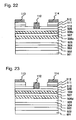
- Fig. 22 is a diagrammatic sectional view of a further modification of the second embodiment of the FET in accordance with the present invention.
- This modification of the second embodiment is characterized in that the undoped Al 0.5 Ga 0.5 As barrier layer 506 having the film thickness of 4nm and the undoped Al 0.5 Ga 0.5 As barrier layer 508 having the film thickness of 4nm shown in Fig. 16, are replaced with an undoped Al 0.8 Ga 0.2 As barrier layer 506c having a film thickness of 5nm and an undoped Al 0.4 Ga 0.6 As barrier layer 508c having a film thickness of 4nm, respectively.
- the barrier layers in the double barrier structure are asymmetrical in the film thickness and in the composition
- This modification of the second embodiment has the threshold voltage of +0.3V.
- the gate forward direction rising voltage is +1.4V, and the maximum drain current is as large as 340mA/mm.
- the barrier layer near to the channel layer has the aluminum composition ratio higher than that in the barrier layer remote from the channel layer.
- Fig. 23 is a diagrammatic sectional view of a still further modification of the second embodiment of the FET in accordance with the present invention.
- This modification of the second embodiment is characterized in that the undoped Al 0.5 Ga 0.5 As barrier layer 506 having the film thickness of 4nm shown in Fig. 16, is replaced with an (Al 0.3 Ga 0.7 ) 0.5 In 0.5 P barrier layer 506d doped with Si at an impurity concentration of 4 ⁇ 10 18 cm -3 and having a film thickness of 4nm.
- the barrier layers in the double barrier structure become asymmetrical by doping the impurity into one of the barrier layers in the double barrier structure.
- This modification of the second embodiment has the threshold voltage of +0.3V.
- the gate forward direction rising voltage is +1.4V, and the maximum drain current is as large as 340mA/mm.
- the impurity is doped into the barrier layer near to the channel layer. This is equivalent to the fact that the distance between the channel layer and the n-type impurity doped layer becomes short. Therefore, the amount of carriers accumulated in the channel layer increases, so that the maximum drain current increases.
- the two semiconductor barrier layers can be formed of different materials.
- the field effect transistor in accordance with the present invention can have a large maximum drain current, even if an ion implantation is not carried out for lowering the contact resistance.
- a contact ion implantation can be carried out in the field effect transistor in accordance with the present invention. In this case, of course, a further large drain current can be obtained.
- Fig. 24 is a diagrammatic sectional view of a further modification of the first embodiment of the FET in accordance with the present invention in which a contact ion implantation can be carried out.
- elements corresponding to those shown in Fig. 1 are given the same reference numbers, and explanation will be omitted.
- the reference number 117 designates a contact ion implanted region.
- This modification of the first embodiment has the threshold voltage of +0.3V.
- the gate forward direction rising voltage is +1.1V, and the maximum drain current is as large as 380mA/mm, which becomes larger than that in the heterojunction FET shown in Fig. 1 by about 10%.
- the contact ion implanted region 117 can be formed by forming a mask having an opening corresponding to each of the source electrode and the drain electrode, by ion implanting Si ions at an acceleration energy of 150keV and a dose of 2 ⁇ 10 13 cm -2 and by carrying out an activating heat-treatment at a temperature of 800°C for a time of five seconds.
- Fig. 25 is a diagrammatic sectional view of a further modification of the second embodiment of the FET in accordance with the present invention in which a contact ion implantation can be carried out.
- elements corresponding to those shown in Fig. 16 are given the same reference numbers, and explanation will be omitted.
- the reference number 117 designates a contact ion implanted region.
- This modification of the second embodiment has the threshold voltage of +0.3V.
- the gate forward direction rising voltage is +1.2V, and the maximum drain current is as large as 370mA/mm, which becomes larger than that in the heterojunction FET shown in Fig. 1 by about 10%.
- Fig. 26 is a diagrammatic sectional view of a still further modification of the first embodiment of the FET in accordance with the present invention, in which a GaAs layer 118 doped with an n-type impurity at an impurity concentration of 4 ⁇ 10 18 cm -3 is epitaxially grown in a pair of ohmic contact regions in the heterojunction FET of the first embodiment of the present invention, and the source electrode 113 and the drain electrode 114 are formed on the GaAs layer 118.
- This modification of the first embodiment has the threshold voltage of +0.3V.
- the gate forward direction rising voltage is +1.1V, and the maximum drain current is as large as 380mA/mm, which becomes larger than that in the heterojunction FET shown in Fig. 1 by about 10%.
- the contact resistance between the channel layer and each of the source electrode and the drain electrode is reduced by removing the barrier layers directly under the ohmic electrodes and by epitaxially growing a semiconductor layer doped with an n-type impurity at a high impurity concentration. As a result, a further large drain current can be obtained.
- a potential barrier formed by a semiconductor barrier layer inserted between the channel layer and the upper electron supplying layer effectively functions as a barrier when a forward direction gate bias is applied, so that a gate leak current is reduced in the forward direction gate biasing condition and a gate forward direction rising voltage can be elevated.
- a semiconductor barrier layer inserted between the channel layer and the upper electron supplying layer but also another semiconductor barrier layer inserted between the upper electron supplying layer and the gate electrode.
- the film thickness of the semiconductor barrier layer is not less than 3nm but not greater than 10nm, or alternatively, not less than 3nm but not greater than the critical film thickness when the critical film thickness is less than 10nm.
- a channel layer side portion of the semiconductor barrier layer is in an undoped condition, but a gate electrode side portion of the semiconductor barrier layer is doped with an n-type impurity, so that a portion of the semiconductor barrier layer functions as an electron supplying layer. Accordingly, since the distance between the upper electron supplying layer and the channel layer becomes further short, a very large number of electrons are accumulated in the channel layer, so that a maximum drain current can be further increased.
- a portion or all of the semiconductor barrier layer near to a channel layer is doped with an n-type impurity.
- the distance between the upper electron supplying layer and the channel layer becomes further short, a very large number of electrons are accumulated in the channel layer, so that a maximum drain current can be further increased.
- the electron supplying layers can be located under and above the channel layer and near to the channel layer, a large number of electrons can be accumulated in the channel layer, so that a maximum drain current can be further increased.
Landscapes
- Junction Field-Effect Transistors (AREA)
Applications Claiming Priority (2)
| Application Number | Priority Date | Filing Date | Title |
|---|---|---|---|
| JP36105799A JP2001177089A (ja) | 1999-12-20 | 1999-12-20 | 電界効果トランジスタ |
| JP36105799 | 1999-12-20 |
Publications (1)
| Publication Number | Publication Date |
|---|---|
| EP1134810A2 true EP1134810A2 (de) | 2001-09-19 |
Family
ID=18472018
Family Applications (1)
| Application Number | Title | Priority Date | Filing Date |
|---|---|---|---|
| EP00127979A Withdrawn EP1134810A2 (de) | 1999-12-20 | 2000-12-20 | Feldeffekttransistor |
Country Status (5)
| Country | Link |
|---|---|
| US (1) | US20010005016A1 (de) |
| EP (1) | EP1134810A2 (de) |
| JP (1) | JP2001177089A (de) |
| KR (1) | KR20010067474A (de) |
| CN (1) | CN1306311A (de) |
Cited By (4)
| Publication number | Priority date | Publication date | Assignee | Title |
|---|---|---|---|---|
| WO2003071607A1 (en) * | 2002-02-21 | 2003-08-28 | The Furukawa Electric Co., Ltd. | GaN FIELD-EFFECT TRANSISTOR |
| US9543424B2 (en) | 2011-07-18 | 2017-01-10 | Epigan Nv | Method for growing III-V epitaxial layers and semiconductor structure |
| US10192986B1 (en) | 2012-05-23 | 2019-01-29 | Hrl Laboratories, Llc | HEMT GaN device with a non-uniform lateral two dimensional electron gas profile and method of manufacturing the same |
| US10700201B2 (en) | 2012-05-23 | 2020-06-30 | Hrl Laboratories, Llc | HEMT GaN device with a non-uniform lateral two dimensional electron gas profile and method of manufacturing the same |
Families Citing this family (11)
| Publication number | Priority date | Publication date | Assignee | Title |
|---|---|---|---|---|
| JP2004179318A (ja) * | 2002-11-26 | 2004-06-24 | Nec Compound Semiconductor Devices Ltd | 接合型電界効果トランジスタ及びその製造方法 |
| JP4610858B2 (ja) | 2003-02-12 | 2011-01-12 | 住友化学株式会社 | 化合物半導体エピタキシャル基板 |
| JP2005340417A (ja) * | 2004-05-26 | 2005-12-08 | Mitsubishi Electric Corp | ヘテロ接合電界効果型半導体装置 |
| CN100508212C (zh) * | 2004-06-24 | 2009-07-01 | 日本电气株式会社 | 半导体器件 |
| JP2007103425A (ja) * | 2005-09-30 | 2007-04-19 | Oki Electric Ind Co Ltd | 化合物半導体からなる電界効果トランジスタ |
| JP2009081177A (ja) * | 2007-09-25 | 2009-04-16 | Nec Electronics Corp | 電界効果トランジスタ、半導体チップ及び半導体装置 |
| CN101877360A (zh) * | 2009-04-30 | 2010-11-03 | 台湾积体电路制造股份有限公司 | 集成电路结构 |
| US8258543B2 (en) * | 2009-12-07 | 2012-09-04 | Intel Corporation | Quantum-well-based semiconductor devices |
| WO2014147706A1 (ja) | 2013-03-18 | 2014-09-25 | 富士通株式会社 | 半導体装置 |
| JP6905197B2 (ja) * | 2017-12-20 | 2021-07-21 | 富士通株式会社 | 化合物半導体装置及びその製造方法 |
| CN120152333B (zh) * | 2025-05-14 | 2025-09-12 | 中科(深圳)无线半导体有限公司 | 一种phemt器件外延结构及其制备方法 |
-
1999
- 1999-12-20 JP JP36105799A patent/JP2001177089A/ja active Pending
-
2000
- 2000-12-20 EP EP00127979A patent/EP1134810A2/de not_active Withdrawn
- 2000-12-20 US US09/739,696 patent/US20010005016A1/en not_active Abandoned
- 2000-12-20 KR KR1020000078951A patent/KR20010067474A/ko not_active Ceased
- 2000-12-20 CN CN00136104A patent/CN1306311A/zh active Pending
Cited By (5)
| Publication number | Priority date | Publication date | Assignee | Title |
|---|---|---|---|---|
| WO2003071607A1 (en) * | 2002-02-21 | 2003-08-28 | The Furukawa Electric Co., Ltd. | GaN FIELD-EFFECT TRANSISTOR |
| US7038253B2 (en) | 2002-02-21 | 2006-05-02 | The Furukawa Electric Co., Ltd. | GaN-based field effect transistor of a normally-off type |
| US9543424B2 (en) | 2011-07-18 | 2017-01-10 | Epigan Nv | Method for growing III-V epitaxial layers and semiconductor structure |
| US10192986B1 (en) | 2012-05-23 | 2019-01-29 | Hrl Laboratories, Llc | HEMT GaN device with a non-uniform lateral two dimensional electron gas profile and method of manufacturing the same |
| US10700201B2 (en) | 2012-05-23 | 2020-06-30 | Hrl Laboratories, Llc | HEMT GaN device with a non-uniform lateral two dimensional electron gas profile and method of manufacturing the same |
Also Published As
| Publication number | Publication date |
|---|---|
| US20010005016A1 (en) | 2001-06-28 |
| JP2001177089A (ja) | 2001-06-29 |
| CN1306311A (zh) | 2001-08-01 |
| KR20010067474A (ko) | 2001-07-12 |
Similar Documents
| Publication | Publication Date | Title |
|---|---|---|
| US5060031A (en) | Complementary heterojunction field effect transistor with an anisotype N+ ga-channel devices | |
| EP1134810A2 (de) | Feldeffekttransistor | |
| US7071499B2 (en) | Heterojunction field effect type semiconductor device having high gate turn-on voltage and low on-resistance and its manufacturing method | |
| US20160293746A1 (en) | Semiconductor device | |
| US20030157776A1 (en) | Methods of fabricating aluminum gallium nitride/gallium nitride high electron mobility transistors having a gate contact on a gallium nitride based cap segment | |
| US20010013604A1 (en) | Compound semiconductor device and process for fabricating the same | |
| EP0477515A1 (de) | Heteroübergangsfeldeffekttransistor mit einer atomaren Schicht im Kanalbereich | |
| US20210066488A1 (en) | Silcon carbide field-effect transistors | |
| US5596211A (en) | Field effect transistor having a graded bandgap InGaAsP channel formed of a two-dimensional electron gas | |
| US5907164A (en) | InAlAs/InGaAs heterojunction field effect type semiconductor device | |
| EP0482726B1 (de) | Heteroübergangsfeldeffekttransistor | |
| US6291842B1 (en) | Field effect transistor | |
| EP0613189A2 (de) | Feldeffekttransistor-Kanalstruktur und Verfahren zur Herstellung | |
| US4866491A (en) | Heterojunction field effect transistor having gate threshold voltage capability | |
| KR950003946B1 (ko) | 전계효과트랜지스터 | |
| US11894454B2 (en) | Silicon carbide field-effect transistors | |
| JP2661556B2 (ja) | 電界効果型半導体装置 | |
| US5206528A (en) | Compound semiconductor field effect transistor having a gate insulator formed of insulative superlattice layer | |
| US5945693A (en) | Field-effect transistor | |
| KR102543619B1 (ko) | 금속 산화물 반도체 소자 및 그 제조방법 | |
| CN115692491B (zh) | Iii族氮化物增强型hemt器件及其制作方法 | |
| JPH08139105A (ja) | 電界効果型半導体装置 | |
| JP3054216B2 (ja) | 半導体装置 | |
| JP2500459B2 (ja) | ヘテロ接合電界効果トランジスタ | |
| EP0718890A1 (de) | Feldeffekt-Transistor |
Legal Events
| Date | Code | Title | Description |
|---|---|---|---|
| PUAI | Public reference made under article 153(3) epc to a published international application that has entered the european phase |
Free format text: ORIGINAL CODE: 0009012 |
|
| AK | Designated contracting states |
Kind code of ref document: A2 Designated state(s): AT BE CH CY DE DK ES FI FR GB GR IE IT LI LU MC NL PT SE TR |
|
| AX | Request for extension of the european patent |
Free format text: AL;LT;LV;MK;RO;SI |
|
| STAA | Information on the status of an ep patent application or granted ep patent |
Free format text: STATUS: THE APPLICATION HAS BEEN WITHDRAWN |
|
| 18W | Application withdrawn |
Effective date: 20030605 |