EP1132967A2 - Image-pickup apparatus, fabrication method thereof, and camera system - Google Patents
Image-pickup apparatus, fabrication method thereof, and camera system Download PDFInfo
- Publication number
- EP1132967A2 EP1132967A2 EP01101750A EP01101750A EP1132967A2 EP 1132967 A2 EP1132967 A2 EP 1132967A2 EP 01101750 A EP01101750 A EP 01101750A EP 01101750 A EP01101750 A EP 01101750A EP 1132967 A2 EP1132967 A2 EP 1132967A2
- Authority
- EP
- European Patent Office
- Prior art keywords
- image
- pickup device
- pickup
- retaining member
- optical system
- Prior art date
- Legal status (The legal status is an assumption and is not a legal conclusion. Google has not performed a legal analysis and makes no representation as to the accuracy of the status listed.)
- Granted
Links
Images




Classifications
-
- H—ELECTRICITY
- H10—SEMICONDUCTOR DEVICES; ELECTRIC SOLID-STATE DEVICES NOT OTHERWISE PROVIDED FOR
- H10F—INORGANIC SEMICONDUCTOR DEVICES SENSITIVE TO INFRARED RADIATION, LIGHT, ELECTROMAGNETIC RADIATION OF SHORTER WAVELENGTH OR CORPUSCULAR RADIATION
- H10F39/00—Integrated devices, or assemblies of multiple devices, comprising at least one element covered by group H10F30/00, e.g. radiation detectors comprising photodiode arrays
- H10F39/011—Manufacture or treatment of image sensors covered by group H10F39/12
-
- H—ELECTRICITY
- H04—ELECTRIC COMMUNICATION TECHNIQUE
- H04N—PICTORIAL COMMUNICATION, e.g. TELEVISION
- H04N23/00—Cameras or camera modules comprising electronic image sensors; Control thereof
- H04N23/50—Constructional details
- H04N23/54—Mounting of pick-up tubes, electronic image sensors, deviation or focusing coils
-
- H—ELECTRICITY
- H04—ELECTRIC COMMUNICATION TECHNIQUE
- H04N—PICTORIAL COMMUNICATION, e.g. TELEVISION
- H04N23/00—Cameras or camera modules comprising electronic image sensors; Control thereof
- H04N23/80—Camera processing pipelines; Components thereof
- H04N23/81—Camera processing pipelines; Components thereof for suppressing or minimising disturbance in the image signal generation
-
- H—ELECTRICITY
- H04—ELECTRIC COMMUNICATION TECHNIQUE
- H04N—PICTORIAL COMMUNICATION, e.g. TELEVISION
- H04N25/00—Circuitry of solid-state image sensors [SSIS]; Control thereof
- H04N25/60—Noise processing, e.g. detecting, correcting, reducing or removing noise
- H04N25/61—Noise processing, e.g. detecting, correcting, reducing or removing noise the noise originating only from the lens unit, e.g. flare, shading, vignetting or "cos4"
-
- H—ELECTRICITY
- H10—SEMICONDUCTOR DEVICES; ELECTRIC SOLID-STATE DEVICES NOT OTHERWISE PROVIDED FOR
- H10F—INORGANIC SEMICONDUCTOR DEVICES SENSITIVE TO INFRARED RADIATION, LIGHT, ELECTROMAGNETIC RADIATION OF SHORTER WAVELENGTH OR CORPUSCULAR RADIATION
- H10F39/00—Integrated devices, or assemblies of multiple devices, comprising at least one element covered by group H10F30/00, e.g. radiation detectors comprising photodiode arrays
- H10F39/80—Constructional details of image sensors
-
- H—ELECTRICITY
- H10—SEMICONDUCTOR DEVICES; ELECTRIC SOLID-STATE DEVICES NOT OTHERWISE PROVIDED FOR
- H10F—INORGANIC SEMICONDUCTOR DEVICES SENSITIVE TO INFRARED RADIATION, LIGHT, ELECTROMAGNETIC RADIATION OF SHORTER WAVELENGTH OR CORPUSCULAR RADIATION
- H10F39/00—Integrated devices, or assemblies of multiple devices, comprising at least one element covered by group H10F30/00, e.g. radiation detectors comprising photodiode arrays
- H10F39/80—Constructional details of image sensors
- H10F39/806—Optical elements or arrangements associated with the image sensors
Definitions
- the present invention relates to an image-pickup apparatus including an image-pickup device, a method of fabricating the image-pickup apparatus, and a camera system using the image-pickup apparatus.
- image-pickup devices used for image-pickup apparatuses are fabricated by forming image-pickup elements on a semiconductor wafer by semiconductor fabrication processes, and cut the semiconductor wafer into chips.
- the image-pickup device thus obtained has a flat-plate shape having a large thickness as a whole, and thereby it exhibits a rigid, non-deformable shape characteristic.
- an image-pickup plane formed on a principal plane of the image-pickup device is planar along the principal plane.
- an object is imaged on an image-pickup plane of an image-pickup device through imaging lenses built in an imaging optical system.
- FIG. 17 is a schematic side view showing a state in which an image-pickup device is arranged in combination with an imaging optical system.
- a diaphragm portion 51A is integrally formed at the leading end of a lens barrel 51, and two imaging lenses 52A and 52B and an intermediate diaphragm 51B are built in the lens barrel 51.
- An image-pickup device 53 is arranged relative to the imaging optical system having the above configuration, with the central portion of the image-pickup device 53 aligned to the optical axis (optical center) of the imaging optical system.
- curvature of field In the case of imaging an object through imaging lenses, there generally occurs a lens aberration called "curvature of field". As shown in FIG. 18, if a focal point is adjusted to P1 at a central portion of the image-pickup device 53, the focal point becomes P2 at a peripheral portion of the image-pickup device 53 by the effect of the above-described curvature of field, to cause a deviation in focal point between the central portion and the peripheral portion of the image-pickup device 53. As a result, there occurs degradation of image-pickup characteristics such as unevenness in image quality between the central portion and the peripheral portion of the image-pickup device 53.
- the correction of a lens aberration by an imaging optical system puts a large load on the design of the imaging optical system including lenses, and since the load on the design of the imaging optical system becomes larger with an increase in corrected amount of a lens aberration, the production tolerance of each lens becomes correspondingly stricter. Further, if the amount to be corrected of a lens aberration becomes larger to some extent, there is a possibility that the lens aberration cannot be sufficiently corrected, to thereby cause degradation of image quality.
- An object of the present invention is to provide an image-pickup apparatus allowed to suitably cope with a lens aberration occurring in an imaging optical system, a method of fabricating the image-pickup apparatus, and a camera system using the image-pickup apparatus.
- an image-pickup apparatus including: an image-pickup device having a flexible shape characteristic; and a retaining member for retaining the image-pickup device in a specific shape.
- a camera system using an image-pickup apparatus including: an image-pickup device having a flexible shape characteristic; and a retaining member for retaining the image-pickup device in a specific shape.
- a method of fabricating an image-pickup apparatus including an image-pickup device having a flexible shape characteristic and a retaining member for retaining the image-pickup device in a specific shape, the method including the step of: making the retaining member retain the image-pickup device in a specific shape by disposing the image-pickup device on the retaining member, and in such a state, blowing air to the image-pickup device from an image-pickup plane side of the image-pickup device or sucking air from the opposed side to the image-pickup plane through the retaining member.
- the image-pickup device having a flexible shape characteristic is retained by the retaining member, when the image-pickup device is used in combination with an imaging optical system, a lens aberration occurring in the imaging optical system can be suitably corrected by making the retaining member retain the image-pickup device in a state in which the image-pickup device is curved in the thickness direction.
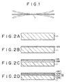
- FIG. 1 is a view illustrating a structure of an image-pickup device used for an image-pickup apparatus according to the present invention.
- an image-pickup device 1 is formed in a very thin film structure by a production method to be described later, and has a flexible shape characteristic or freely deformable characteristic as a whole.
- the image-pickup device 1 has a thickness (which is a thickness of a semiconductor device) in a range of 100 ⁇ m or less, preferably, 50 ⁇ m or less, more preferably, 20 ⁇ m or less.
- the thickness of the image-pickup device 1 is the thickness of only a device portion, and therefore, if a flexible resin sheet or the like is stuck on the back surface of the device, the entire thickness becomes the total of the thickness of the semiconductor device and the thickness of the resin sheet or the like.
- the image-pickup device 1 can be obtained in accordance with one of known thin film semiconductor fabrication methods proposed by the present applicant, for example, disclosed in Japanese Patent Laid-open Nos. Hei 9-255487, Hei 10-135500, Hei 10-270670, Hei 10-256362, and Hei 11-68133.
- One example of the production method will be described below.
- a semiconductor substrate 11 made from Si, GaAs, GaP, GaN, SiGe, or the like is prepared.
- a wafer shaped substrate made from single crystal Si heavily doped with boron B and having a resistivity of 0.01 to 0.02 ⁇ cm is preferably used as the semiconductor substrate 11.
- the front surface of the semiconductor substrate 11 is subjected to anodic conversion treatment, to form a porous layer including a separation layer on the front surface of the semiconductor substrate 11.
- the anodic conversion treatment for the semiconductor substrate 11 is performed in an electrolytic solution containing hydrogen fluoride and ethanol, or containing hydrogen fluoride and methanol.
- the anodic conversion treatment can be performed by a known method, for example, disclosed in Ito, et al., Anodic Conversion treatment for Porous Si, Surface Technology, Vol. 46, No. 5, pp. 8-13, 1995.
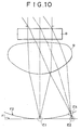
- the anodic conversion treatment can be performed, for example, by a double cell method using double cells schematically shown in FIG. 3. Referring to FIG. 3, there is shown an electrolytic solution cell 21 of a double cell structure having a first cell 21A and a second cell 21B.
- a semiconductor substrate 11 on which a porous layer is to be formed is disposed between both the cells 21A and 21B, and a pair of platinum electrodes 23A and 23B to which a direct voltage source 22 is connected are put in both the cells 21A and 21B, respectively.
- Each of the first and second cells 21A and 21B of the electrolytic solution cell 21 is filled with an electrolytic solution 24 containing hydrogen fluoride HF and ethanol C 2 H 5 OH or containing hydrogen fluoride HF and methanol CH 3 OH.
- the semiconductor substrate 11 is disposed between the first and second cells 21A and 21B with both surfaces of the substrate 11 being in contact with the electrolytic solutions 24 in the first and second cells 21A and 21B, and both the electrodes 23A and 23B are dipped in the electrolytic solutions 24 in the first and second cells 21A and 21B, respectively.
- the electrode 23A dipped in the electrolytic solution 24 in the first cell 21A on the front surface side of the semiconductor substrate 11 on which a porous layer is to be formed is taken as a negative electrode, and a current is carried from the direct voltage source 22 between both the electrodes 23A and 23B.
- a the semiconductor substrate 11 is taken as an anode side and the electrode 23A is taken as a cathode side, with a result that the front surface, opposed to the electrode 23A side, of the semiconductor substrate 11 is eroded, whereby a porous layer is formed on the front surface of the semiconductor substrate 11.
- the double cell method is advantageous in eliminating the need of forming an ohmic electrode on the semiconductor substrate, thereby preventing entrapment of impurities from the ohmic electrode into the semiconductor substrate. It should be noted that the anodic conversion treatment is not necessarily carried out by the double cell method but may be carried out by a single cell method.
- the porous layer to be formed on the surface of the semiconductor substrate is configured to have a plurality of layers different in porosity by repeating the anodic conversion treatment in a plurality of steps, for example, by performing a first anodic conversion treatment at a low current density, a second anodic conversion treatment at a relatively high current density, and a third anodic conversion treatment at a high current density.
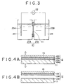
- a current is carried at a low current density of 1 mA/cm 2 for 8 min, to form a porous surface layer 12S on the front surface of the semiconductor substrate 11 as shown in FIG. 2B.
- the current-carrying is stopped once and then a current is carried at a relatively high current density of 7 mA/cm 2 for 8 min, to form an intermediate porosity layer 12M being higher in porosity and larger in pore diameter than the surface layer 12S as shown in FIG. 2C.
- the current-carrying is stopped once and then a current is carried at a high current density of 80 mA/cm 2 for 0.3 sec; the current-carrying is stopped for 1 min and then a current is carried again at the high current density of 80 mA/cm 2 ; and the current-carrying is stopped for 1 min and then a current is carried again at the high current density of 80 mA/cm 2 , to form a high porosity layer 12H which is higher in porosity than the intermediate porosity layer 12M and which is inserted in the intermediate porosity layer 12M, that is, held between the two-divided parts of the intermediate porosity layer 12M as shown in FIG. 2D.
- the high porosity layer 12H functions as a separation layer.
- the porous layer 12 composed of the stack of the surface layer 12S, the upper intermediate porosity layer 12M, the high porosity layer (separation layer) 12H, and the lower intermediate porosity layer 12M, is formed on the front surface of the semiconductor substrate 11.
- the formation of the porous layer 12 including a separation layer on the front surface of the semiconductor substrate 11 is not necessarily performed by the above-described anodic conversion treatment, but may be performed by an ion implantation method.
- a semiconductor film for forming the image-pickup device 1 is formed on the semiconductor substrate 11 on which the porous layer 12 has been formed as described above.
- the semiconductor substrate 11 on which the porous layer 12 has been formed is put in a normal pressure Si epitaxial growth system, and is annealed in an H 2 atmosphere. The annealing is performed by heating the semiconductor substrate 11 from room temperature to 1030°C for a temperature rising time of about 20 min and keeping the semiconductor substrate 11 at 1030°C for about 30 min.
- the front surface of the porous layer 12 is smoothened, and a portion, near the interface between the high porosity layer 12H and each of the intermediate porosity layers 12M, of the high porosity layer 12H becomes weaker, and thereby the high porosity layer 12H becomes a separation layer capable of certainly separating a semiconductor film to be described later from the semiconductor substrate 11.
- the temperature of the semiconductor substrate 11 is dropped from the annealing temperature of 1030°C to 1000°C, followed by supply of a SiH 4 gas and B 2 H 6 gas in the epitaxial growth system, and Si is epitaxially grown on the semiconductor substrate 11 by a CVD (Chemical Vapor Deposition) process, to form a semiconductor film 13 made from single crystal Si or polycrystalline Si on the surface layer 12S of the porous layer 12 as shown in FIG. 4A.
- a CVD Chemical Vapor Deposition
- an image-pickup device is formed on the semiconductor film 13 made from Si in accordance with a usual semiconductor fabrication process (for example, a CCD fabrication process).
- a resin sheet (not shown) is stuck on the semiconductor film 13, on which the image-pickup device has been formed, with an adhesive strength higher than a separation strength of the separation layer 12H of the porous film 12, and then external forces are applied in the directions shown by arrows in FIG. 4A for separating the resin sheet.
- the brittle separation layer that is, the high porosity layer 12H is broken, whereby the semiconductor film 13 is separated (or peeled) from the semiconductor substrate 11 as shown in FIG. 4B.
- the surface layer 12S and the intermediate porosity layer 12M of the porous layer 12, remaining on the semiconductor film 13, are removed by etching. In this way, the image-pickup device 1 being very thin and having a flexible shape characteristic, which is shown in FIG. 1, is obtained.
- the semiconductor substrate 11 is reused, with a result that it is possible to significantly reduce the material cost, save the resource, and reduce the fabrication cost in fabrication of the image-pickup device 1.
- FIG. 5 is a schematic side view showing a configuration of an image-pickup apparatus using the image-pickup device 1.
- the image-pickup device 1 is retained by a retaining member 2 with an image-pickup plane (not shown) directed upwardly.
- the retaining member 2 is a plate-shaped member having an outer dimension larger than that of the image-pickup device 1, which member is made from a metal material, a ceramic material, a resin material, or a composite material thereof.
- a plurality of projections 3 are integrally formed on the upper surface of the retaining member 2, or separately formed and joined to the upper surface of the retaining member 2. These projections 3 are provided on the image-pickup device 1 having a rectangular shape in a plan view in such a manner as to be located at four corners of the image-pickup device 1 or located along two opposed sides of the image-pickup device 1.
- the image-pickup device 1 is retained by the retaining member 2 in such a manner that the peripheral edge thereof is in contact with the projections 3 and the central portion thereof is in contact with the upper surface of the retaining member 2. In such a state, the image-pickup device 1 is retained in a state being curved in the thickness direction because of the flexible shape characteristic of the image-pickup device 1.
- the image-pickup device 1 thus retained is fixed to the retaining member 2 by bonding the image-pickup device 1 to the retaining member 2 at the contact portions such as the projections 3 by using an adhesive. Further, the image-pickup device 1 is retained in a state in which an image-pickup plane (not shown) is curved in a recessed shape.
- the image-pickup apparatus including these image-pickup device 1 and the retaining member 2 is suitably used for a camera system by combination with an imaging optical system to be described later and further with a signal processing system.
- the image-pickup device 1 is retained in a state being curved by providing the projections 3 on the upper surface of the retaining member 2; however, the retaining configuration of the image-pickup device 1 is not limited thereto.
- the image-pickup device 1 can be retained in a state being curved by integrally forming a stepped recess 4 in the upper surface of the retaining member 2, and placing the image-pickup device 1 on the retaining member 2 while bringing the image-pickup device 1 into contact with the bottom of the recess 4 and the upper surface of the retaining member 2.
- the image-pickup device 1 can be retained in a state being curved by forming a recessed plane portion 5, which is curved in a recessed shape, in the upper surface of the retaining member 2, and placing the image-pickup device 1 on the retaining member 2 while bringing the back surface (opposed to the front surface, that is, the image-pickup plane) of the image-pickup device 1 uniformly into face-contact with the recessed plane portion 5.
- the image-pickup device 1 is retained in such a manner as to be curved along the shape of the recessed plane portion 5 of the retaining member 2, the curved shape of the image-pickup device 1 in the retained state can be accurately set.
- FIG. 8 is a schematic side view showing a state in which the image-pickup device of the present invention is arranged in combination of an imaging optical system.
- a diaphragm portion 6A is integrally formed at the leading end of a lens barrel 6, and two imaging lenses 7A and 7B and an intermediate diaphragm portion 6B are built in the lens barrel 6.
- the image-pickup device 1 is arranged relative to the imaging optical system configured as described above, with the central portion thereof aligned to the optical axis (optical center) of the imaging optical system.
- the image-pickup plane (not shown) of the image-pickup device 1 is located in such a manner as to form a recessed plane to light rays made incident through the imaging lenses 7A and 7B, and the like.
- a lens aberration occurring in the imaging optical system can be suitably corrected by the image-pickup device 1.
- a focal point P1 (at the central portion of the image-pickup device 1) and a focal point P2 (at the peripheral portion of the image-pickup device 1) of light rays made incident through the intermediate diaphragm portion 6B, the imaging lens 7B, and the like of the imaging optical system are deviated from each other in the direction along the optical axis (vertical direction in FIG. 9) by the effect of the above-described lens aberration.
- the central portion of the image-pickup device 1 can be set to the focal point P1 and the peripheral portion of the image-pickup device 1 can be set to the focal point P2.
- focal points of light rays made incident from the imaging optical system can be located overall on the image pickup-plane (not shown) of the image-pickup device 1, it is possible to eliminate the unevenness of image quality due to a deviation in focal point.
- a lens aberration occurring in the imaging optical system can be corrected by both the imaging optical system and the image-pickup apparatus, loads on the design and manufacture of the imaging optical system can be significantly reduced as compared with the conventional correction of a lens aberration only by the imaging optical system.
- a lens aberration cannot be sufficiently corrected only by the imaging optical system, it can be sufficiently corrected by combination with the image-pickup apparatus, with a result that it is possible to certainly prevent degradation of image quality due to a lens aberration.
- the incident angle of light rays at the peripheral portion of the image-pickup device 1 can be made small as compared with a related art image-pickup device. Accordingly, it is possible to make small a reduction in incident light quantity at the peripheral portion of the image-pickup device 1, and to equalize the incident angle of light over the image-pickup device 1 and hence to correct the shading.
- the shape of the image-pickup device 1 in the retained state can be freely set in correspondence with an amount to be corrected of a lens aberration occurring in the imaging optical system, and it can be also set in correspondence with an average amount to be corrected of a plurality of lens aberrations in consideration of a variation therebetween. Further, the imaging optical system (including imaging lenses) can be designed in matching with the shape of the image-pickup device 1 in the retained state.
- the image-pickup device 1 can be most desirably arranged relative to the imaging optical system by obtaining shape data capable of suitably correcting a lens aberration through simulation based on lens design data, and forming the recessed plane portion 4 shown in FIG. 7 in the upper surface of the retaining member 2 on the basis of the shape data.
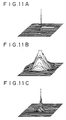
- FIG. 10 is a comparative view showing a state in which the image-pickup device of the present invention and a related art image-pickup device are.arranged in combination with an imaging optical system.
- an optical filter 8 and an imaging lens 9 form an imaging optical system.
- the related art image-pickup device is arranged in a flat plane F1 and the image-pickup device of the present invention is arranged in a curved plane F2.
- FIGS. 12A and 12B show data on the resolving power of the related art image-pickup device
- FIG. 12B shows data on the resolving power of the image-pickup device of the present invention.
- a solid line shows the resolving power at the central portion of the device (optical center axis);
- a broken line shows the resolving power in the radial direction at the peripheral portion of the device;
- a dash line shows the resolving power in the direction perpendicular to the radial direction at the peripheral portion of the device.
- the resolving power is high.
- the resolving power is sharply dropped at a relatively low frequency, while at the peripheral portion of the image-pickup device of the present invention, the resolving power is very gently dropped.
- the image pickup device 1 is retained in such a manner as to be curved in a recessed plane with respect to light rays made incident through an imaging optical system; however, the retaining configuration of the image-pickup device 1 of the present invention is not limited thereto. For example, as shown in FIG.
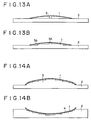
- the image-pickup device 1 can be retained by the retaining member 2 in such a manner as to be curved in a projecting plane with respect to the above-described incident light rays by providing projections 3 on the upper surface of the retaining member 2 and placing the image-pickup device 1 on the retaining member 2 in such a manner that the central portion of the image-pickup device 1 is in contact with the projections 3 and the peripheral portion of the image-pickup device 1 is in contact with the upper surface of the retaining member 2.
- the image-pickup device 1 can be similarly retained by the retaining member 2 in such a manner as to be curved in a projecting plane by providing a first projection 3A and a second projection 3B on the upper surface of the retaining member 2 and placing the image-pickup device 1 on the retaining member 2 in such a manner that the central portion and intermediate portion of the image-pickup device 1 are in contact with the projections 3A and 3B respectively and the peripheral portion of the image-pickup device 1 is in contact with the upper surface of the retaining member 2.
- the image-pickup device 1 can be similarly retained by the retaining member 2 in such a manner as to be curved in a projecting plane by providing a stepped projection 3 having a plurality of steps on the upper surface of the retaining member 2 and placing the image-pickup device 1 on the retaining member 2 in such a manner that the image-pickup device 1 is in contact with the steps of the stepped projection 3. Further, as shown in FIG. 14A, the image-pickup device 1 can be similarly retained by the retaining member 2 in such a manner as to be curved in a projecting plane by providing a stepped projection 3 having a plurality of steps on the upper surface of the retaining member 2 and placing the image-pickup device 1 on the retaining member 2 in such a manner that the image-pickup device 1 is in contact with the steps of the stepped projection 3. Further, as shown in FIG.
- the image-pickup device 1 can be retained by the retaining member 2 in such a manner as to be curved in a recessed plane by providing a stepped recess 4 having a plurality of steps in the upper surface of the retaining member 2 and placing the image-pickup device 1 on the retaining member 2 in such a manner that the image-pickup device 1 is in contact with the steps of the stepped recess 4.
- each of the steps of the projection 3 and the recess 4 formed on and in the retaining member 2 is formed by a plane parallel to the thickness direction of the retaining member 2 and a plane perpendicular thereto, with a result that the stepped projection 3 or the stepped recess 4 can be easily formed on or in the retaining member 2 by machining and further the image-pickup device 1 can be retained in a projecting or recessed plane closer to the ideal projecting or recessed plane.
- the recessed plane portion is formed in the upper surface of the retaining member 2; however, a projecting plane portion (not shown), curved in a projecting shape, may be formed on the upper surface of the retaining member 2.
- the image-pickup device 1 can be retained in such a manner as to be curved along the projecting plane of the retaining member 2.
- the shape of the image-pickup device 1 retained by the retaining member 2 is not limited to a curved shape (for example, recessed or projecting shape), but may be variously changed depending on the application of the image-pickup device 1. For example, by forming two independent image-pickup planes on the principal plane of the image-pickup device 1 and retaining the image-pickup device 1 in an approximately V-shape or an approximately inverse V-shape so as to tilt each image-pickup plane at a specific angle, objects in the different directions can be simultaneously imaged by the same image-pickup device 1.
- the front surface of the image-pickup device 1 may be damaged by the contact with the jig.
- the function of the image-pickup device 1 may be impaired.
- the peripheral portion, around the image-pickup plane, of the image-pickup device is pressed by using pins or the like, since a local pressure is applied to the image-pickup device 1, a wiring portion of the precise image-pickup device 1 may be damaged.
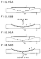
- the image-pickup device 1 is retained on the retaining member by using the following assembling method.
- the image-pickup device 1 is placed over the retaining member 2 in such a manner as to face to the stepped recess 4 and in such a state, as shown in FIG. 15B, air is blown in the direction shown by an arrow, that is, in the direction from the image-pickup plane (upper surface of the device) side to the image-pickup device 1.
- air may be blown only to the central portion of the image-pickup device 1, or may be blown to both the central portion and the peripheral portion of the image-pickup device 1.
- the blow of air causes an air pressure applied to the image-pickup device 1, so that the image-pickup device 1 is deformed in a state in which the back surface of the device 1 is in contact with the steps of the stepped recess 4.
- air present on the back surface (lower surface) of the image-pickup device 1 can be escaped to the outside through the communication hole 2A, with a result that the air pressure by blow of air can be effectively applied to the image-pickup device 1.
- the image-pickup device 1 can be retained on the retaining member 2 in such a manner as to be curved in a recessed shape without pressing the principal plane of the image-pickup device 1 with a jig, and further the image-pickup device 1 can be accurately retained on the retaining member 2 because the image-pickup device 1 can be desirably fitted to the stepped recess 4 formed in the retaining member 2.
- the assembling method using an air pressure by blow of air can be also applied to the methods of fabricating the image-pickup devices shown in FIGS. 5 to 7, FIGS. 13A and 13B, and FIG. 14A. Additionally, in the case where the image-pickup device 1 is retained on the retaining member 2 in such a manner as to be curved in a projecting shape as shown in each of FIGS. 13A and 13B, and FIG. 14A, air must be blown to the peripheral portion of the image-pickup device 1, or to both the central portion and the peripheral portion of the image-pickup device 1.
- FIGS. 16A and 16B Another assembling method using an air pressure by suction of air will be described below.
- a communication hole 2A is provided in the bottom surface of the recess 4 of the retaining member 2, wherein the image-pickup device 1 is placed over the retaining member 2, and in such a state, air is sucked from the communication hole 2A.
- the atmospheric pressure on the back surface side (opposed to the image-pickup plane) of the image-pickup device 1 is reduced by suction of air through the communication hole 2A.
- the image-pickup device 1 is deformed with a suction force caused by the reduction in atmospheric pressure.
- the image-pickup device 1 can be retained on the retaining member 2 in such a manner as to be curved in a recessed shape without pressing the principal plane of the image-pickup device 1 with a jig, and further the image-pickup device 1 can be accurately retained on the retaining member 2 because the image-pickup device 1 can be desirably fitted to the stepped recess 4 formed in the retaining member 2.
- the assembling method using an air pressure by suction of air can be also applied to the methods of fabricating the image-pickup devices shown in FIGS. 5 to 7.
- the image-pickup device having a flexible shape characteristic is retained by the retaining member in a specific shape curved in the thickness direction, when the image-pickup apparatus is used in combination with an imaging optical system, a lens aberration occurring in the imaging optical system can be suitably corrected by the image-pickup apparatus, with a result that it is possible to significantly reduce loads on the design and manufacture of the imaging optical system (particularly, imaging lenses), and to certainly prevent degradation of image quality due to a lens aberration.
Landscapes
- Engineering & Computer Science (AREA)
- Multimedia (AREA)
- Signal Processing (AREA)
- Solid State Image Pick-Up Elements (AREA)
- Studio Devices (AREA)
- Transforming Light Signals Into Electric Signals (AREA)
- Lenses (AREA)
Abstract
Description
Claims (5)
- An image-pickup apparatus comprising:an image-pickup device having a flexible shape characteristic; anda retaining member for retaining said image-pickup device in a specific shape.
- An image-pickup apparatus according to claim 1, wherein said retaining member retains said image-pickup device in a state in which said image-pickup device is curved in the thickness direction.
- An image-pickup apparatus according to claim 2, wherein said image-pickup device is retained on said retaining member in a state in which an image-pickup plane of said image-pickup device is curved in a recessed shape.
- A camera system using an image-pickup apparatus, said image-pickup apparatus comprising:an image-pickup device having a flexible shape characteristic; anda retaining member for retaining said image-pickup device in a specific shape.
- A method of fabricating an image-pickup apparatus including an image-pickup device having a flexible shape characteristic and a retaining member for retaining the image-pickup device in a specific shape, said method comprising the step of:
making the retaining member retain the image-pickup device in a specific shape by disposing the image-pickup device on the retaining member, and in such a state, blowing air to the image-pickup device from an image-pickup plane side of the image-pickup device or sucking air from the opposed side to the image-pickup plane through the retaining member.
Priority Applications (1)
| Application Number | Priority Date | Filing Date | Title |
|---|---|---|---|
| EP10009710A EP2256809A3 (en) | 2000-01-27 | 2001-01-25 | Image-pickup apparatus, fabrication method thereof, and camera system |
Applications Claiming Priority (4)
| Application Number | Priority Date | Filing Date | Title |
|---|---|---|---|
| JP2000018246 | 2000-01-27 | ||
| JP2000018246 | 2000-01-27 | ||
| JP2000096965 | 2000-03-31 | ||
| JP2000096965A JP4604307B2 (en) | 2000-01-27 | 2000-03-31 | Imaging apparatus, method for manufacturing the same, and camera system |
Related Child Applications (1)
| Application Number | Title | Priority Date | Filing Date |
|---|---|---|---|
| EP10009710.4 Division-Into | 2010-09-16 |
Publications (3)
| Publication Number | Publication Date |
|---|---|
| EP1132967A2 true EP1132967A2 (en) | 2001-09-12 |
| EP1132967A3 EP1132967A3 (en) | 2004-04-28 |
| EP1132967B1 EP1132967B1 (en) | 2012-10-31 |
Family
ID=26584258
Family Applications (2)
| Application Number | Title | Priority Date | Filing Date |
|---|---|---|---|
| EP10009710A Withdrawn EP2256809A3 (en) | 2000-01-27 | 2001-01-25 | Image-pickup apparatus, fabrication method thereof, and camera system |
| EP01101750A Expired - Lifetime EP1132967B1 (en) | 2000-01-27 | 2001-01-25 | Method of fabrication a curved image-pickup apparatus |
Family Applications Before (1)
| Application Number | Title | Priority Date | Filing Date |
|---|---|---|---|
| EP10009710A Withdrawn EP2256809A3 (en) | 2000-01-27 | 2001-01-25 | Image-pickup apparatus, fabrication method thereof, and camera system |
Country Status (3)
| Country | Link |
|---|---|
| US (1) | US6486917B2 (en) |
| EP (2) | EP2256809A3 (en) |
| JP (1) | JP4604307B2 (en) |
Cited By (10)
| Publication number | Priority date | Publication date | Assignee | Title |
|---|---|---|---|---|
| EP1202327A1 (en) * | 2000-10-31 | 2002-05-02 | Disco Corporation | Semiconductor device |
| FR2966936A1 (en) * | 2010-11-02 | 2012-05-04 | Commissariat Energie Atomique | OPTICAL IMAGING SYSTEM FOR A CONCAVE SPHERICAL SURFACE |
| EP2437298A4 (en) * | 2009-05-29 | 2013-01-09 | Nec Toshiba Space Sys Ltd | IMAGE READING DEVICE AND METHOD FOR CONFIGURING IMAGE READING ELEMENT |
| WO2013161216A1 (en) * | 2012-04-26 | 2013-10-31 | Sony Corporation | Imaging apparatus and electronic system |
| WO2016161222A1 (en) * | 2015-04-02 | 2016-10-06 | Microsoft Technology Licensing, Llc | Bending semiconductor chip in molds having radially varying curvature |
| WO2016161223A1 (en) * | 2015-04-02 | 2016-10-06 | Microsoft Technology Licensing, Llc | Free-edge semiconductor chip bending |
| US9859314B2 (en) | 2014-09-19 | 2018-01-02 | Microsoft Technology Licensing, Llc | Image sensor bending by induced substrate swelling |
| US10062727B2 (en) | 2016-09-09 | 2018-08-28 | Microsoft Technology Licensing, Llc | Strain relieving die for curved image sensors |
| US10361235B2 (en) | 2016-11-23 | 2019-07-23 | Industrial Technology Research Institute | Image sensor |
| US10373995B2 (en) | 2014-09-19 | 2019-08-06 | Microsoft Technology Licensing, Llc | Image sensor bending using tension |
Families Citing this family (33)
| Publication number | Priority date | Publication date | Assignee | Title |
|---|---|---|---|---|
| US6618093B1 (en) * | 1998-01-15 | 2003-09-09 | Chauncey F. Levy | Distortion-free imaging device having curved photosensor |
| DE10004891C2 (en) * | 2000-02-04 | 2002-10-31 | Astrium Gmbh | Focal area and detector for optoelectronic image recording systems, manufacturing process and optoelectronic image recording system |
| JP2002300480A (en) * | 2001-03-29 | 2002-10-11 | Fuji Photo Optical Co Ltd | Electronic camera |
| US6759277B1 (en) * | 2003-02-27 | 2004-07-06 | Sharp Laboratories Of America, Inc. | Crystalline silicon die array and method for assembling crystalline silicon sheets onto substrates |
| JP2005278133A (en) * | 2003-07-03 | 2005-10-06 | Fuji Photo Film Co Ltd | Solid-state imaging device and optical apparatus |
| US7786421B2 (en) * | 2003-09-12 | 2010-08-31 | California Institute Of Technology | Solid-state curved focal plane arrays |
| DE102005047149A1 (en) * | 2005-09-30 | 2007-04-12 | Osram Opto Semiconductors Gmbh | Epitaxial substrate, component manufactured therewith and corresponding manufacturing methods |
| JP2007109848A (en) * | 2005-10-13 | 2007-04-26 | Fujifilm Corp | Solid-state imaging device, manufacturing method thereof, and manufacturing device thereof |
| US9041851B2 (en) * | 2005-11-15 | 2015-05-26 | The Trustees Of Princeton University | Organic electronic detectors and methods of fabrication |
| JP2008092532A (en) * | 2006-10-05 | 2008-04-17 | Matsushita Electric Ind Co Ltd | IMAGING DEVICE, MANUFACTURING METHOD THEREOF, AND MOBILE TELEPHONE DEVICE |
| DE102010019805A1 (en) * | 2010-05-06 | 2011-11-10 | Z/I Imaging Ltd. | Camera, in particular for taking aerial photographs from airplanes |
| JP2013084880A (en) * | 2011-09-27 | 2013-05-09 | Toshiba Corp | Solid state imaging device, solid state imaging element, and method for manufacturing solid state imaging element |
| JP5705140B2 (en) * | 2011-09-27 | 2015-04-22 | 株式会社東芝 | Solid-state imaging device and method for manufacturing solid-state imaging device |
| CN104272715A (en) | 2012-05-01 | 2015-01-07 | 中央工程株式会社 | Stereo camera and stereo camera system |
| JP6135109B2 (en) * | 2012-12-07 | 2017-05-31 | ソニー株式会社 | Solid-state imaging device, manufacturing method of solid-state imaging device, and electronic apparatus |
| JP2015026946A (en) * | 2013-07-25 | 2015-02-05 | 株式会社東芝 | The camera module |
| EP3084824A4 (en) | 2013-12-19 | 2017-08-16 | Intel Corporation | Flexibly-wrapped integrated circuit die |
| RU2623697C2 (en) | 2014-09-26 | 2017-06-28 | Интел Корпорейшн | Architecture of creating flexible bodies |
| JP6230124B2 (en) | 2014-12-05 | 2017-11-15 | 太陽誘電株式会社 | Imaging device built-in substrate, manufacturing method thereof, and imaging device |
| JP2016134857A (en) | 2015-01-21 | 2016-07-25 | キヤノン株式会社 | Imaging device and control method therefor, program, storage medium |
| JP6463159B2 (en) | 2015-02-05 | 2019-01-30 | キヤノン株式会社 | IMAGING DEVICE, ITS CONTROL METHOD, PROGRAM, AND STORAGE MEDIUM |
| US10139619B2 (en) | 2015-02-12 | 2018-11-27 | Optiz, Inc. | Back side illumination image sensor with non-planar optical interface |
| US10032870B2 (en) * | 2015-03-12 | 2018-07-24 | Globalfoundries Inc. | Low defect III-V semiconductor template on porous silicon |
| JP6525687B2 (en) * | 2015-04-03 | 2019-06-05 | キヤノン株式会社 | Imaging device and imaging device |
| WO2016166890A1 (en) * | 2015-04-17 | 2016-10-20 | オリンパス株式会社 | Imaging device |
| FR3073322B1 (en) * | 2017-11-07 | 2021-12-03 | Commissariat Energie Atomique | PROCESS FOR MAKING AT LEAST ONE CURVED ELECTRONIC CIRCUIT |
| CN110944099B (en) * | 2018-09-21 | 2021-08-10 | 南昌欧菲光电技术有限公司 | Photosensitive assembly manufacturing method, photosensitive assembly, camera module and intelligent terminal |
| CN112311974B (en) * | 2019-08-01 | 2025-06-10 | 宁波舜宇光电信息有限公司 | Photosensitive assembly, camera module and manufacturing method thereof |
| EP3998768B1 (en) * | 2019-08-01 | 2025-04-30 | Ningbo Sunny Opotech Co., Ltd. | CAMERA MODULE AND LIGHT-SENSITIVE ARRANGEMENT AND MANUFACTURING METHOD THEREFOR |
| CN112311973B (en) * | 2019-08-01 | 2025-04-08 | 宁波舜宇光电信息有限公司 | Photosensitive component and camera module and manufacturing method thereof |
| JP2021108427A (en) * | 2019-12-27 | 2021-07-29 | ソニーセミコンダクタソリューションズ株式会社 | Imaging device and manufacturing method of imaging device |
| US12514003B2 (en) * | 2020-04-02 | 2025-12-30 | Hrl Laboratories, Llc | Curved imaging sensor package with petal patterned substrate |
| CN116959997A (en) * | 2022-04-18 | 2023-10-27 | 浙江清华柔性电子技术研究院 | A chip module and its manufacturing method |
Family Cites Families (27)
| Publication number | Priority date | Publication date | Assignee | Title |
|---|---|---|---|---|
| JPS5396720A (en) * | 1977-02-04 | 1978-08-24 | Hitachi Ltd | Solid image pickup element |
| JPS5829274A (en) * | 1981-08-14 | 1983-02-21 | Olympus Optical Co Ltd | Image pickup device |
| JPS60235103A (en) * | 1984-05-09 | 1985-11-21 | Mitsui Toatsu Chem Inc | Focus control method |
| JPH0741323B2 (en) * | 1985-12-11 | 1995-05-10 | 株式会社日立製作所 | Manufacturing method of metal spherical shell parts |
| JPH0683405B2 (en) * | 1987-12-17 | 1994-10-19 | 日本電気株式会社 | Wide area high resolution imaging method |
| JPH01202989A (en) * | 1988-02-09 | 1989-08-15 | Nec Corp | Solid-state image pickup device |
| US5400072A (en) * | 1988-12-23 | 1995-03-21 | Hitachi, Ltd. | Video camera unit having an airtight mounting arrangement for an image sensor chip |
| US5184176A (en) * | 1990-10-08 | 1993-02-02 | Canon Kabushiki Kaisha | Projection exposure apparatus with an aberration compensation device of a projection lens |
| EP0510267A1 (en) * | 1991-04-24 | 1992-10-28 | Gec-Marconi Limited | Imaging array devices and staring array imaging systems |
| EP0546797B1 (en) * | 1991-12-09 | 1997-08-06 | Sharp Kabushiki Kaisha | Liquid crystal light valve and information processor having liquid crystal light valve |
| US5416344A (en) * | 1992-07-29 | 1995-05-16 | Nikon Corporation | Solid state imaging device and method for producing the same |
| JPH06133229A (en) * | 1992-10-16 | 1994-05-13 | Fuji Photo Optical Co Ltd | Solid-state image pickup element having micro lens |
| JP2699841B2 (en) * | 1993-12-10 | 1998-01-19 | 日本電気株式会社 | Solid-state imaging device |
| US6122009A (en) * | 1995-05-31 | 2000-09-19 | Sony Corporation | Image pickup apparatus fabrication method thereof image pickup adaptor apparatus signal processing apparatus signal processing method thereof information processing apparatus and information processing method |
| DE19532119A1 (en) * | 1995-08-31 | 1997-03-06 | Burghard Schmachtenberg | Photographic or similar apparatus |
| DE19605984C1 (en) * | 1996-02-17 | 1997-09-11 | Karlsruhe Forschzent | Variable optical lens for microsystem |
| JPH10135500A (en) | 1996-03-18 | 1998-05-22 | Sony Corp | Method for manufacturing thin film semiconductor, solar cell and light emitting element |
| JPH09255487A (en) | 1996-03-18 | 1997-09-30 | Sony Corp | Manufacturing method of thin film semiconductor |
| US5880777A (en) * | 1996-04-15 | 1999-03-09 | Massachusetts Institute Of Technology | Low-light-level imaging and image processing |
| US6208468B1 (en) * | 1996-06-11 | 2001-03-27 | Olympus Optical Co., Ltd. | Image-forming optical system and apparatus using the same |
| US6078359A (en) * | 1996-07-15 | 2000-06-20 | The Regents Of The University Of California | Vacuum compatible miniature CCD camera head |
| JP2809215B2 (en) * | 1996-09-26 | 1998-10-08 | 日本電気株式会社 | Solid-state imaging camera |
| JP3951340B2 (en) | 1997-03-17 | 2007-08-01 | ソニー株式会社 | Semiconductor substrate and method of manufacturing semiconductor substrate and thin film semiconductor |
| JP3963030B2 (en) | 1997-03-26 | 2007-08-22 | ソニー株式会社 | Thin film semiconductor manufacturing method |
| US6072204A (en) * | 1997-06-23 | 2000-06-06 | Scientific Imaging Technologies, Inc. | Thinned CCD |
| JPH1168133A (en) | 1997-08-21 | 1999-03-09 | Sony Corp | Thin film element module and method of manufacturing the same |
| JP4156154B2 (en) * | 1999-11-26 | 2008-09-24 | 富士フイルム株式会社 | Solid-state imaging device |
-
2000
- 2000-03-31 JP JP2000096965A patent/JP4604307B2/en not_active Expired - Lifetime
-
2001
- 2001-01-23 US US09/767,977 patent/US6486917B2/en not_active Expired - Lifetime
- 2001-01-25 EP EP10009710A patent/EP2256809A3/en not_active Withdrawn
- 2001-01-25 EP EP01101750A patent/EP1132967B1/en not_active Expired - Lifetime
Cited By (15)
| Publication number | Priority date | Publication date | Assignee | Title |
|---|---|---|---|---|
| EP1202327A1 (en) * | 2000-10-31 | 2002-05-02 | Disco Corporation | Semiconductor device |
| EP2437298A4 (en) * | 2009-05-29 | 2013-01-09 | Nec Toshiba Space Sys Ltd | IMAGE READING DEVICE AND METHOD FOR CONFIGURING IMAGE READING ELEMENT |
| FR2966936A1 (en) * | 2010-11-02 | 2012-05-04 | Commissariat Energie Atomique | OPTICAL IMAGING SYSTEM FOR A CONCAVE SPHERICAL SURFACE |
| WO2012059676A3 (en) * | 2010-11-02 | 2012-08-30 | Commissariat A L'energie Atomique Et Aux Energies Alternatives | Optical system for forming an image on a concave spherical surface |
| US9146384B2 (en) | 2010-11-02 | 2015-09-29 | Commissariat à l'énergie atomique et aux énergies alternatives | Optical system for forming an image on a concave spherical surface |
| US9496301B2 (en) | 2012-04-26 | 2016-11-15 | Sony Corporation | Imaging apparatus and electronic system |
| WO2013161216A1 (en) * | 2012-04-26 | 2013-10-31 | Sony Corporation | Imaging apparatus and electronic system |
| US9859314B2 (en) | 2014-09-19 | 2018-01-02 | Microsoft Technology Licensing, Llc | Image sensor bending by induced substrate swelling |
| US10373995B2 (en) | 2014-09-19 | 2019-08-06 | Microsoft Technology Licensing, Llc | Image sensor bending using tension |
| WO2016161223A1 (en) * | 2015-04-02 | 2016-10-06 | Microsoft Technology Licensing, Llc | Free-edge semiconductor chip bending |
| WO2016161222A1 (en) * | 2015-04-02 | 2016-10-06 | Microsoft Technology Licensing, Llc | Bending semiconductor chip in molds having radially varying curvature |
| US9870927B2 (en) | 2015-04-02 | 2018-01-16 | Microsoft Technology Licensing, Llc | Free-edge semiconductor chip bending |
| US10304900B2 (en) | 2015-04-02 | 2019-05-28 | Microsoft Technology Licensing, Llc | Bending semiconductor chip in molds having radially varying curvature |
| US10062727B2 (en) | 2016-09-09 | 2018-08-28 | Microsoft Technology Licensing, Llc | Strain relieving die for curved image sensors |
| US10361235B2 (en) | 2016-11-23 | 2019-07-23 | Industrial Technology Research Institute | Image sensor |
Also Published As
| Publication number | Publication date |
|---|---|
| JP4604307B2 (en) | 2011-01-05 |
| EP1132967A3 (en) | 2004-04-28 |
| EP2256809A2 (en) | 2010-12-01 |
| EP1132967B1 (en) | 2012-10-31 |
| JP2001284564A (en) | 2001-10-12 |
| US20010040639A1 (en) | 2001-11-15 |
| EP2256809A3 (en) | 2012-08-29 |
| US6486917B2 (en) | 2002-11-26 |
Similar Documents
| Publication | Publication Date | Title |
|---|---|---|
| US6486917B2 (en) | Image-pickup apparatus, fabrication method thereof, and camera system | |
| US7022585B2 (en) | Method for making thin film devices intended for solar cells or silicon-on-insulator (SOI) applications | |
| JP7821862B2 (en) | Semiconductor device manufacturing method | |
| US6791072B1 (en) | Method and apparatus for forming curved image sensor module | |
| JP6570009B2 (en) | Integration of epitaxial lift-off solar cells with a small parabolic concentrator by printing method | |
| US6881650B2 (en) | Method for forming SOI substrate | |
| US9217206B2 (en) | Enhanced porosification | |
| CN105870141B (en) | Curved surface image sensor system and its manufacturing method | |
| EP2403003B1 (en) | Method for manufacturing thin film compound solar cell | |
| CN101512768A (en) | Camera system and associated methods | |
| CN101432888B (en) | Ultra lightweight photovoltaic device and method for its manufacture | |
| KR101700728B1 (en) | Manufacture of multijunction solar cell devices | |
| JP5146056B2 (en) | Semiconductor device manufacturing method and semiconductor device support device | |
| CN111081531B (en) | Epitaxial layer stripping method | |
| JP5980540B2 (en) | Method for producing thin film compound solar cell with interconnector, method for producing thin film compound solar cell string, and method for producing thin film compound solar cell array | |
| JP2000299489A (en) | Photoelectric conversion element and light receiver | |
| CN104205364B (en) | The manufacture of multijunction solar cell device | |
| US20130240030A1 (en) | Method for fabricating thin photovoltaic cells | |
| KR20240071043A (en) | Press Method of Electrode Assembly for Lithium Secondary Battery and Apparatus thereof | |
| CN112216767B (en) | Fabrication of semiconductor photosensitive device | |
| EP1385200A2 (en) | Method for making thin film devices intended for solar cells or SOI applications | |
| JP6769013B2 (en) | Processed circuit board with embedded mirror | |
| CN114725132B (en) | Image sensor and method of forming the same | |
| JPH10270670A (en) | Method of manufacturing thin film semiconductor | |
| CN104247048B (en) | Fabrication of multi-junction solar cell devices |
Legal Events
| Date | Code | Title | Description |
|---|---|---|---|
| PUAI | Public reference made under article 153(3) epc to a published international application that has entered the european phase |
Free format text: ORIGINAL CODE: 0009012 |
|
| AK | Designated contracting states |
Kind code of ref document: A2 Designated state(s): AT BE CH CY DE DK ES FI FR GB GR IE IT LI LU MC NL PT SE TR |
|
| AX | Request for extension of the european patent |
Free format text: AL;LT;LV;MK;RO;SI |
|
| PUAL | Search report despatched |
Free format text: ORIGINAL CODE: 0009013 |
|
| AK | Designated contracting states |
Kind code of ref document: A3 Designated state(s): AT BE CH CY DE DK ES FI FR GB GR IE IT LI LU MC NL PT SE TR |
|
| AX | Request for extension of the european patent |
Extension state: AL LT LV MK RO SI |
|
| 17P | Request for examination filed |
Effective date: 20041001 |
|
| AKX | Designation fees paid |
Designated state(s): DE FR GB |
|
| RIC1 | Information provided on ipc code assigned before grant |
Ipc: H01L 27/146 20060101AFI20120320BHEP |
|
| RTI1 | Title (correction) |
Free format text: METHOD OF FABRICATION A CURVED IMAGE-PICKUP APPARATUS |
|
| GRAP | Despatch of communication of intention to grant a patent |
Free format text: ORIGINAL CODE: EPIDOSNIGR1 |
|
| GRAS | Grant fee paid |
Free format text: ORIGINAL CODE: EPIDOSNIGR3 |
|
| GRAA | (expected) grant |
Free format text: ORIGINAL CODE: 0009210 |
|
| AK | Designated contracting states |
Kind code of ref document: B1 Designated state(s): DE FR GB |
|
| RAP1 | Party data changed (applicant data changed or rights of an application transferred) |
Owner name: SONY CORPORATION |
|
| REG | Reference to a national code |
Ref country code: GB Ref legal event code: FG4D Ref country code: DE Ref legal event code: R081 Ref document number: 60147293 Country of ref document: DE Owner name: SONY SEMICONDUCTOR SOLUTIONS CORP., ATSUGI-SHI, JP Free format text: FORMER OWNER: SONY CORPORATION, TOKIO/TOKYO, JP |
|
| RIN1 | Information on inventor provided before grant (corrected) |
Inventor name: IWASAKI, MASANORI, C/O SONY CORPORATION |
|
| REG | Reference to a national code |
Ref country code: DE Ref legal event code: R096 Ref document number: 60147293 Country of ref document: DE Effective date: 20121227 |
|
| PLBE | No opposition filed within time limit |
Free format text: ORIGINAL CODE: 0009261 |
|
| STAA | Information on the status of an ep patent application or granted ep patent |
Free format text: STATUS: NO OPPOSITION FILED WITHIN TIME LIMIT |
|
| 26N | No opposition filed |
Effective date: 20130801 |
|
| REG | Reference to a national code |
Ref country code: DE Ref legal event code: R097 Ref document number: 60147293 Country of ref document: DE Effective date: 20130801 |
|
| PGFP | Annual fee paid to national office [announced via postgrant information from national office to epo] |
Ref country code: FR Payment date: 20140123 Year of fee payment: 14 |
|
| PGFP | Annual fee paid to national office [announced via postgrant information from national office to epo] |
Ref country code: GB Payment date: 20140121 Year of fee payment: 14 |
|
| GBPC | Gb: european patent ceased through non-payment of renewal fee |
Effective date: 20150125 |
|
| PG25 | Lapsed in a contracting state [announced via postgrant information from national office to epo] |
Ref country code: GB Free format text: LAPSE BECAUSE OF NON-PAYMENT OF DUE FEES Effective date: 20150125 |
|
| REG | Reference to a national code |
Ref country code: FR Ref legal event code: ST Effective date: 20150930 |
|
| PG25 | Lapsed in a contracting state [announced via postgrant information from national office to epo] |
Ref country code: FR Free format text: LAPSE BECAUSE OF NON-PAYMENT OF DUE FEES Effective date: 20150202 |
|
| REG | Reference to a national code |
Ref country code: DE Ref legal event code: R082 Ref document number: 60147293 Country of ref document: DE Representative=s name: MUELLER HOFFMANN & PARTNER PATENTANWAELTE MBB, DE Ref country code: DE Ref legal event code: R081 Ref document number: 60147293 Country of ref document: DE Owner name: SONY SEMICONDUCTOR SOLUTIONS CORP., ATSUGI-SHI, JP Free format text: FORMER OWNER: SONY CORPORATION, TOKIO/TOKYO, JP |
|
| PGFP | Annual fee paid to national office [announced via postgrant information from national office to epo] |
Ref country code: DE Payment date: 20200121 Year of fee payment: 20 |
|
| REG | Reference to a national code |
Ref country code: DE Ref legal event code: R071 Ref document number: 60147293 Country of ref document: DE |