EP1132793A1 - Bias-Schaltung - Google Patents
Bias-Schaltung Download PDFInfo
- Publication number
- EP1132793A1 EP1132793A1 EP01105553A EP01105553A EP1132793A1 EP 1132793 A1 EP1132793 A1 EP 1132793A1 EP 01105553 A EP01105553 A EP 01105553A EP 01105553 A EP01105553 A EP 01105553A EP 1132793 A1 EP1132793 A1 EP 1132793A1
- Authority
- EP
- European Patent Office
- Prior art keywords
- voltage
- circuit arrangement
- vcc
- supply voltage
- transistor
- Prior art date
- Legal status (The legal status is an assumption and is not a legal conclusion. Google has not performed a legal analysis and makes no representation as to the accuracy of the status listed.)
- Granted
Links
- 238000010586 diagram Methods 0.000 description 6
- 238000010276 construction Methods 0.000 description 2
- 239000000463 material Substances 0.000 description 2
- 239000004065 semiconductor Substances 0.000 description 2
- 229910052710 silicon Inorganic materials 0.000 description 2
- 239000010703 silicon Substances 0.000 description 2
- 230000006978 adaptation Effects 0.000 description 1
- 230000015556 catabolic process Effects 0.000 description 1
- 230000001419 dependent effect Effects 0.000 description 1
- 238000005516 engineering process Methods 0.000 description 1
- 230000001105 regulatory effect Effects 0.000 description 1
- 238000004088 simulation Methods 0.000 description 1
Images

Classifications
-
- G—PHYSICS
- G05—CONTROLLING; REGULATING
- G05F—SYSTEMS FOR REGULATING ELECTRIC OR MAGNETIC VARIABLES
- G05F3/00—Non-retroactive systems for regulating electric variables by using an uncontrolled element, or an uncontrolled combination of elements, such element or such combination having self-regulating properties
- G05F3/02—Regulating voltage or current
- G05F3/08—Regulating voltage or current wherein the variable is DC
- G05F3/10—Regulating voltage or current wherein the variable is DC using uncontrolled devices with non-linear characteristics
- G05F3/16—Regulating voltage or current wherein the variable is DC using uncontrolled devices with non-linear characteristics being semiconductor devices
- G05F3/20—Regulating voltage or current wherein the variable is DC using uncontrolled devices with non-linear characteristics being semiconductor devices using diode- transistor combinations
- G05F3/22—Regulating voltage or current wherein the variable is DC using uncontrolled devices with non-linear characteristics being semiconductor devices using diode- transistor combinations wherein the transistors are of the bipolar type only
- G05F3/222—Regulating voltage or current wherein the variable is DC using uncontrolled devices with non-linear characteristics being semiconductor devices using diode- transistor combinations wherein the transistors are of the bipolar type only with compensation for device parameters, e.g. Early effect, gain, manufacturing process, or external variations, e.g. temperature, loading, supply voltage
Definitions
- the present invention relates to a circuit arrangement, in particular a bias circuit for generating a useful voltage (VO).
- VO useful voltage
- Circuit arrangements of the type mentioned are usually used to generate a certain, defined useful voltage, which are then made available to other useful circuit circuits becomes. It is often desirable that the generated Useful voltage as independent of external conditions as possible, such as for example the temperature, various technology parameters and also of the value of the circuit arrangement available set supply voltage.
- a circuit arrangement for generating a useful voltage (V0), the regardless of the actual value of the supply voltage (VCC) is provided with an apparatus for generating a Reference voltage and with one or more collector current source (s), which are / are each formed from a transistor, the base of the transistor being connected to the output of the device is connected to generate a reference voltage, the emitter of the transistor is connected to ground and the collector of Transistor with a voltage source for the supply voltage (VCC) v is connected.
- V0 useful voltage
- VCC supply voltage
- the circuit arrangement according to the invention makes it possible that the full useful voltage (V0) is always provided can be.
- the useful voltage (V0) generated in this way can be, for example, 3 volts.
- the invention is not to a certain level of the generated useful voltage (V0) limited so that useful voltages due to the circuit arrangement (V0) can be generated with any other values.
- circuit arrangement according to the invention requires no pnp transistors, resulting in those described above Disadvantages can be avoided.
- the circuit arrangement initially has one Device for generating a reference voltage. Examples suitable devices will be described later in the description explained in more detail.
- one or more collector power source (s) is connected to the is / are each formed from a transistor.
- the connection of the at least one transistor with the output of the device to generate the reference voltage is done on its basis.
- the emitter of the at least one transistor is connected Ground connected.
- the supply voltage can advantageously be used as ground (VEE) can be used.
- the collector of at least one The transistor has a voltage source for the Supply voltage (VCC) connected.
- This connection of the collector to the voltage source for the Supply voltage (VCC) can be done in different ways.
- the collector directly, for example as an emitter follower, with the voltage source for the supply voltage (VCC) is connected.
- VCC supply voltage
- the Circuit arrangement can be designed in a very simple manner, since the supply voltage is below the breakdown voltage (VCC) no longer have a significant influence on the function of the circuit arrangement.
- the at least one, the collector current source forming transistor, through a resistor is connected. This can be done between the collector of at least a transistor and the voltage source for the supply voltage (VCC) a resistor must be connected.
- This resistance can, for example, as a load resistor, voltage divider or the like.
- Such from the transistor forming the collector current source and the resistance of the circuit part formed behaves like a voltage source independent of the supply voltage (VCC) to generate the useful voltage (V0), which has a corresponding R has internal resistance.
- the resistors used can have a different size. For this you need different collector power sources, each with one corresponding adaptation of the emitter areas of the respective transistor can be realized.
- Transistors may be provided.
- Each collector can each of the transistors its own resistor with the voltage source for the supply voltage (VCC) connected.
- VCC supply voltage
- collector current sources forming transistors are controlled together.
- the device for generating a reference voltage can different ways are formed.
- the device for generating a reference voltage has an operational amplifier.
- the device for generating a reference voltage can be advantageous also have a so-called bandgap circuit.
- a such circuit makes it possible to have a temperature independent Generate useful voltage (V0).
- Bandgap circuits are based on the basic principle that a voltage with negative temperature coefficient to a voltage with a positive temperature coefficient is added such that the temperature coefficient Becomes zero. With integrated bandgap circuits This creates, for example, a tension that corresponds to the band gap distance (Band gap) of the semiconductor material corresponds.
- the Bandgap voltage for silicon is around 1.2 volts.
- a advantageous embodiment for such a bandgap circuit is, for example, in that of the applicant patent application (GR 00 P 8030 DE), the disclosure content in this regard in the description of the present Invention is included.
- VCC supply voltage
- the circuit arrangement according to the invention can preferably be integrated Be designed bipolar circuit.
- V0 useful voltage
- VCC supply voltage
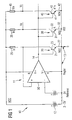
- the circuit arrangement 10 initially has a device 11 for generating a reference voltage, which in the present Example is designed as an operational amplifier 50. That in Operational amplifier 50 generated voltage signal is via a Output 14 of the device 11 for generating the reference voltage passed on to further components of the circuit arrangement 10.
- VCC supply voltage
- the circuit arrangement 10 includes a or multiple collector power sources are provided, each consisting of a transistor is / are formed.
- a total of three collector current sources are shown according to FIG. 1, each formed from a transistor 20, 30, 40 are.
- the number of collector power sources can vary vary according to the application.
- the base 21, 31, 41 of each transistor 20, 30, 40 is with the Output 14 of the device 11 for generating the reference voltage connected.
- the emitter 22, 32, 42 of each transistor 20, 30, 40 is connected to Ground 13, which in the present embodiment is the supply voltage (VEE).
- Collectors 23, 33, 43 of transistors 20, 30, 40 are each with a voltage source 12 connected for the supply voltage (VCC).
- the voltage parts formed from the respective transistors 20, 30, 40 and the resistors 25, 35, 45 behave like a voltage source for the useful voltage (V0) which is independent of the supply voltage (VCC) and has an internal resistance of the value R.
- V0 useful voltage
- VCC supply voltage
- R internal resistance of the value R.
- differently dimensioned voltage sources are required. This can be done by adapting the transistors 20, 30, 40 via their respective emitter areas A. As shown with regard to the transistor 40 and the resistor 45, as the emitter areas A * x increase, the required values of the resistors R / x become ever smaller.
- the individual transistors designed as collector current sources 20, 30, 40 are advantageously controlled together.
- At the resistor 25 can be a so-called "dummy resistor” act that serves to regulate.
- FIG 2 is another embodiment of the circuit arrangement 10 shown, in which the individual elements for simulation purposes have concrete values.
- the resistor 65 has a size of 2 k ⁇ , the resistor 66 a size of 1 k ⁇ , the resistor 67 a size of 10 k ⁇ and the resistor 68 a size of 3 k ⁇ .
- the voltage source 12 provides a supply voltage (VCC) in 3 - 5 volts are available.
- VCC supply voltage
- the emitter base path serves in the present exemplary embodiment of the transistor (T1) 63 and the voltage source (V2) with a value of 2.13 volts, which together is a reference voltage of 3 volts.
- the resistor 25 has in the exemplary embodiment according to FIG. 2 has a value of 2 k ⁇ , while the resistor 35 has a value of 1,120 ⁇ and the resistor 45 has a value of 2k ⁇ .
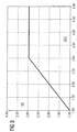
- V0 the generated useful voltage
- VCC supply voltage
- V0 the generated useful voltage
- VCC supply voltage
- V0 stable useful voltage
- the circuit arrangement 10 is thus suitable for a stable and full useful voltage (V0) for a large supply voltage range, the required range of CMOS circuits corresponds to provide.
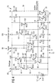
- a circuit arrangement 10 is shown in FIG the reference voltage is generated by a bandgap voltage source 80 becomes.
- Bandgap circuit 80 has a number of transistors 81, 82, 83, 84, 85 and a number of resistors 86, 87, 88.
- the resistor 86 has a value of 2 k ⁇
- resistor 87 has a value of 1,400 ⁇
- the resistor 88 has a value of 2 k ⁇ .
- Via the bandgap circuit 80 becomes a temperature independent reference voltage UB generated when using silicon as a semiconductor material for example, has a value of about 1.2 volts.
- the bandgap voltage UB generated in this way is in one Controller 90, which consists of a transistor 91, 92 and resistors 93, 94, 95 is formed, readjusted as necessary.
- Resistor 93 has a value of 2 k ⁇ , the resistance 94 a value of 240 ⁇ and the resistor 95 a value from 5 k ⁇ .
- Both the controller 90 and the bandgap circuit 80 are part of it the device 11 for generating a reference voltage.
- a multiplier 100 provided for the band gap voltage UB, which consists of a number of transistors 101, 102, 103, 104 and various resistors 105, 106, 107 is constructed.
- Resistor 105 has one Value of 2 k ⁇
- resistor 106 has a value of 2 k ⁇
- the resistor 107 has a value of 5 k ⁇ .
- the Multiplier 100 occurs that generated in bandgap circuit 80 Bandgap voltage UB again, whereby it is about the Factor (1 + R12 / R14) is increased, the resistance R12 around resistor 105 and at resistor R14 is resistor 106. In this way, a total reference voltage reached, for example, 3 volts.
- the reference voltage generated in this way is the Output 14 of the device 11 for generating the reference voltage to the transistors 20, 30 forming the collector current sources forwarded.
- the embodiment shown in Figure 4 are only two transistors 20, 30 shown in their basic structure however correspond to the transistors described in FIGS. 1 and 2, so that with regard to their structure and how they work refer to the explanations for Figures 1 and 2 becomes.
- the collectors of the two transistors 20, 30 are corresponding Resistors 25, 35 with the voltage source 12 for the supply voltage (VCC) connected.
- the two resistors 25, 35 each have a value of 2 k ⁇ .
- the circuit arrangement 10 illustrates that the number of the transistors forming the collector current sources depending on The need and application can be varied.
- the invention is not on a certain number of such transistors, respectively Power sources limited.
- V0 Useful voltage
- VCC supply voltage
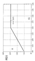
- the voltage curve diagram shown in FIG. 5 shows the value of the useful voltage (V0) both depending on the Supply voltage (VCC) as well as depending on different Temperatures, in the present case 0 ° C, 50 ° C as well 100 ° C.
- VCC Supply voltage
- V0 full useful voltage
Landscapes
- Engineering & Computer Science (AREA)
- Microelectronics & Electronic Packaging (AREA)
- Physics & Mathematics (AREA)
- Nonlinear Science (AREA)
- Electromagnetism (AREA)
- General Physics & Mathematics (AREA)
- Radar, Positioning & Navigation (AREA)
- Automation & Control Theory (AREA)
- Control Of Electrical Variables (AREA)
- Amplifiers (AREA)
Abstract
Description
Claims (9)
- Schaltungsanordnung, insbesondere Bias-Schaltung (10), zum Erzeugen einer Nutzspannung (V0), die unabhängig vom tatsächlichen Wert der Versorgungsspannung (VCC) ist, mit einer Vorrichtung (11) zum Erzeugen einer Referenzspannung und mit einer oder mehreren Kollektor-Stromquelle(n), die jeweils aus einem Transistor (20;30;40) gebildet ist/sind, wobei die Basis (21; 31; 41) des Transistors (20; 30; 40) mit dem Ausgang (14) der Vorrichtung (11) zum Erzeugen einer Referenzspannung verbunden ist, der Emitter (22; 32; 42) des Transistors (20; 30; 40) mit Ground (13) verbunden ist und der Kollektor (23; 33; 43) des Transistors (20; 30; 40) mit einer Spannungsquelle (12) für die Versorgungsspannung (VCC) verbunden ist.
- Schaltungsanordnung nach Anspruch 1, dadurch gekennzeichnet, daß zwischen dem Kollektor (23; 33; 43) des wenigstens einen Transistors (20; 30; 40) und der Spannungsquelle (12) für die Versorgungsspannung (VCC) ein Widerstand (25; 35; 45) geschaltet ist.
- Schaltungsanordnung nach Anspruch 1 oder 2, dadurch gekennzeichnet, daß zwei oder mehr Kollektor-Stromquellen bildende Transistoren (20; 30; 40) vorgesehen sind.
- Schaltungsanordnung nach Anspruch 3, dadurch gekennzeichnet, daß jeder Kollektor (23, 33, 43) jedes der Transistoren (20; 30; 40) über jeweils einen Widerstand (25, 35, 45) mit der Spannungsquelle (12) für Versorgungsspannung (VCC) verbunden ist.
- Schaltungsanordnung nach einem der Ansprüche 1 bis 4, dadurch gekennzeichnet, daß die die Kollektor-Stromquellen bildenden Transistoren (20, 30, 40) gemeinsam gesteuert werden.
- Schaltungsanordnung nach einem der Ansprüche 1 bis 5, dadurch gekennzeichnet, daß die Vorrichtung (11) zum Erzeugen einer Referenzspannung einen Operationsverstärker (50) aufweist.
- Schaltungsanordnung nach einem der Ansprüche 1 bis 6, dadurch gekennzeichnet, daß die Vorrichtung (11) zum Erzeugen einer Referenzspannung eine Bandgap-Schaltung (80) aufweist.
- Schaltungsanordnung nach einem der Ansprüche 1 bis 7, dadurch gekennzeichnet, daß der Wert der Versorgungsspannung (VCC) in einem Bereich zwischen 3 Volt und 5,5 Volt liegt.
- Schaltungsanordnung nach einem der Ansprüche 1 bis 8, dadurch gekennzeichnet, daß diese als integrierte Bipolarschaltung ausgebildet ist.
Applications Claiming Priority (2)
| Application Number | Priority Date | Filing Date | Title |
|---|---|---|---|
| DE10011670A DE10011670A1 (de) | 2000-03-10 | 2000-03-10 | Schaltungsanordnung, insbesondere Bias-Schaltung |
| DE10011670 | 2000-03-10 |
Publications (2)
| Publication Number | Publication Date |
|---|---|
| EP1132793A1 true EP1132793A1 (de) | 2001-09-12 |
| EP1132793B1 EP1132793B1 (de) | 2009-12-23 |
Family
ID=7634208
Family Applications (1)
| Application Number | Title | Priority Date | Filing Date |
|---|---|---|---|
| EP01105553A Expired - Lifetime EP1132793B1 (de) | 2000-03-10 | 2001-03-06 | Bias-Schaltung |
Country Status (3)
| Country | Link |
|---|---|
| EP (1) | EP1132793B1 (de) |
| AT (1) | ATE453144T1 (de) |
| DE (2) | DE10011670A1 (de) |
Citations (5)
| Publication number | Priority date | Publication date | Assignee | Title |
|---|---|---|---|---|
| US3743850A (en) * | 1972-06-12 | 1973-07-03 | Motorola Inc | Integrated current supply circuit |
| EP0524498A2 (de) * | 1991-07-26 | 1993-01-27 | Nec Corporation | Konstantstromquelle |
| EP0745921A1 (de) * | 1995-05-31 | 1996-12-04 | STMicroelectronics S.r.l. | Transistorstromgeneratorstufe für integrierte Analogschaltungen |
| EP0929021A1 (de) * | 1998-01-09 | 1999-07-14 | Nippon Precision Circuits Inc. | Stromversorgungs- und Vorspannungsschaltung |
| US5963082A (en) * | 1996-03-13 | 1999-10-05 | U.S. Philips Corporation | Circuit arrangement for producing a D.C. current |
Family Cites Families (4)
| Publication number | Priority date | Publication date | Assignee | Title |
|---|---|---|---|---|
| JPS59111514A (ja) * | 1982-12-17 | 1984-06-27 | Hitachi Ltd | 半導体集積回路 |
| US5604467A (en) * | 1993-02-11 | 1997-02-18 | Benchmarg Microelectronics | Temperature compensated current source operable to drive a current controlled oscillator |
| US5880624A (en) * | 1994-07-08 | 1999-03-09 | Kabushiki Kaisha Toshiba | Constant potential generating circuit and semiconductor device using same |
| DE19535807C1 (de) * | 1995-09-26 | 1996-10-24 | Siemens Ag | Schaltungsanordnung zur Erzeugung eines Biaspotentials |
-
2000
- 2000-03-10 DE DE10011670A patent/DE10011670A1/de not_active Withdrawn
-
2001
- 2001-03-06 EP EP01105553A patent/EP1132793B1/de not_active Expired - Lifetime
- 2001-03-06 AT AT01105553T patent/ATE453144T1/de not_active IP Right Cessation
- 2001-03-06 DE DE50115269T patent/DE50115269D1/de not_active Expired - Lifetime
Patent Citations (5)
| Publication number | Priority date | Publication date | Assignee | Title |
|---|---|---|---|---|
| US3743850A (en) * | 1972-06-12 | 1973-07-03 | Motorola Inc | Integrated current supply circuit |
| EP0524498A2 (de) * | 1991-07-26 | 1993-01-27 | Nec Corporation | Konstantstromquelle |
| EP0745921A1 (de) * | 1995-05-31 | 1996-12-04 | STMicroelectronics S.r.l. | Transistorstromgeneratorstufe für integrierte Analogschaltungen |
| US5963082A (en) * | 1996-03-13 | 1999-10-05 | U.S. Philips Corporation | Circuit arrangement for producing a D.C. current |
| EP0929021A1 (de) * | 1998-01-09 | 1999-07-14 | Nippon Precision Circuits Inc. | Stromversorgungs- und Vorspannungsschaltung |
Also Published As
| Publication number | Publication date |
|---|---|
| ATE453144T1 (de) | 2010-01-15 |
| EP1132793B1 (de) | 2009-12-23 |
| DE10011670A1 (de) | 2001-09-20 |
| DE50115269D1 (de) | 2010-02-04 |
Similar Documents
| Publication | Publication Date | Title |
|---|---|---|
| DE19530472B4 (de) | Konstantstromschaltung | |
| DE69722530T2 (de) | Stromkreisvorrichtung zum liefern eines gleichstromes | |
| DE1487340B2 (de) | Als inverter wirkender transistorverstaerker mit von temperatur und versorgungsspannungsschwankungen weitgehend unabhaengigem verstaerkungsgrad | |
| DE3420068C2 (de) | ||
| DE102017125831A1 (de) | Temperaturkompensierte Referenzspannungsschaltung | |
| EP0169388B1 (de) | Integrierte Konstantstromquelle | |
| DE69221999T2 (de) | Bezugsstromschleife | |
| WO2003091818A1 (de) | Schaltungsanordnung zur spannungsregelung mittels eines spannungsteilers | |
| DE112021005632T5 (de) | Low-dropout-regler mit begrenzung des einschaltstroms | |
| DE69421083T2 (de) | Schutzschaltung und Verfahren für Leistungstransistor sowie diese verwendender Spannungsregler | |
| DE3433817C2 (de) | ||
| DE3545392C2 (de) | ||
| DE3102398C2 (de) | ||
| DE3043951A1 (de) | Komplementaer-symmetrischer verstaerker | |
| EP0162266A1 (de) | Schaltungsanordnung zur Erzeugung einer temperatur- und versorgungsspannungsunabhängigen Referenzspannung | |
| DE3603799A1 (de) | Stromspiegelschaltung | |
| EP1132793B1 (de) | Bias-Schaltung | |
| DE3243706C1 (de) | ECL-TTL-Signalpegelwandler | |
| EP0961403B1 (de) | Integrierte, temperaturkompensierte Verstärkerschaltung | |
| DE3032675C2 (de) | Tonfrequenz-Leistungsverstärker-Schaltung. | |
| DE2803099C3 (de) | Digital-Analog-Umsetzer in integrierter Schaltungstechnik | |
| DE3118617A1 (de) | Stromspiegelschaltung mit hoher ausgangsimpedanz und niedrigem spannungsverlust | |
| DE2708022C3 (de) | Schaltungsanordnung in integrierter MOS-Technik zur Abgabe einer Konstantspannung | |
| EP1132795B1 (de) | Schaltungsanordnung zum Erzeugen einer Gleichspannung | |
| DE2911171C2 (de) | Schaltung für die Ansteuerung eines Stromquelletransistors |
Legal Events
| Date | Code | Title | Description |
|---|---|---|---|
| PUAI | Public reference made under article 153(3) epc to a published international application that has entered the european phase |
Free format text: ORIGINAL CODE: 0009012 |
|
| AK | Designated contracting states |
Kind code of ref document: A1 Designated state(s): AT BE CH CY DE DK ES FI FR GB GR IE IT LI LU MC NL PT SE TR |
|
| AX | Request for extension of the european patent |
Free format text: AL;LT;LV;MK;RO;SI |
|
| 17P | Request for examination filed |
Effective date: 20020215 |
|
| AKX | Designation fees paid |
Free format text: AT BE CH CY DE DK ES FI FR GB GR IE IT LI LU MC NL PT SE TR |
|
| 17Q | First examination report despatched |
Effective date: 20020508 |
|
| GRAP | Despatch of communication of intention to grant a patent |
Free format text: ORIGINAL CODE: EPIDOSNIGR1 |
|
| GRAS | Grant fee paid |
Free format text: ORIGINAL CODE: EPIDOSNIGR3 |
|
| GRAA | (expected) grant |
Free format text: ORIGINAL CODE: 0009210 |
|
| AK | Designated contracting states |
Kind code of ref document: B1 Designated state(s): AT BE CH CY DE DK ES FI FR GB GR IE IT LI LU MC NL PT SE TR |
|
| REG | Reference to a national code |
Ref country code: GB Ref legal event code: FG4D Free format text: NOT ENGLISH |
|
| REG | Reference to a national code |
Ref country code: CH Ref legal event code: EP |
|
| REG | Reference to a national code |
Ref country code: IE Ref legal event code: FG4D |
|
| REF | Corresponds to: |
Ref document number: 50115269 Country of ref document: DE Date of ref document: 20100204 Kind code of ref document: P |
|
| REG | Reference to a national code |
Ref country code: NL Ref legal event code: VDEP Effective date: 20091223 |
|
| PG25 | Lapsed in a contracting state [announced via postgrant information from national office to epo] |
Ref country code: SE Free format text: LAPSE BECAUSE OF FAILURE TO SUBMIT A TRANSLATION OF THE DESCRIPTION OR TO PAY THE FEE WITHIN THE PRESCRIBED TIME-LIMIT Effective date: 20091223 Ref country code: FI Free format text: LAPSE BECAUSE OF FAILURE TO SUBMIT A TRANSLATION OF THE DESCRIPTION OR TO PAY THE FEE WITHIN THE PRESCRIBED TIME-LIMIT Effective date: 20091223 |
|
| RAP2 | Party data changed (patent owner data changed or rights of a patent transferred) |
Owner name: INFINEON TECHNOLOGIES AG |
|
| REG | Reference to a national code |
Ref country code: IE Ref legal event code: FD4D |
|
| PG25 | Lapsed in a contracting state [announced via postgrant information from national office to epo] |
Ref country code: PT Free format text: LAPSE BECAUSE OF FAILURE TO SUBMIT A TRANSLATION OF THE DESCRIPTION OR TO PAY THE FEE WITHIN THE PRESCRIBED TIME-LIMIT Effective date: 20100423 Ref country code: NL Free format text: LAPSE BECAUSE OF FAILURE TO SUBMIT A TRANSLATION OF THE DESCRIPTION OR TO PAY THE FEE WITHIN THE PRESCRIBED TIME-LIMIT Effective date: 20091223 Ref country code: ES Free format text: LAPSE BECAUSE OF FAILURE TO SUBMIT A TRANSLATION OF THE DESCRIPTION OR TO PAY THE FEE WITHIN THE PRESCRIBED TIME-LIMIT Effective date: 20100403 |
|
| BERE | Be: lapsed |
Owner name: INFINEON TECHNOLOGIES A.G. Effective date: 20100331 |
|
| PG25 | Lapsed in a contracting state [announced via postgrant information from national office to epo] |
Ref country code: MC Free format text: LAPSE BECAUSE OF NON-PAYMENT OF DUE FEES Effective date: 20100331 Ref country code: IE Free format text: LAPSE BECAUSE OF FAILURE TO SUBMIT A TRANSLATION OF THE DESCRIPTION OR TO PAY THE FEE WITHIN THE PRESCRIBED TIME-LIMIT Effective date: 20091223 Ref country code: GR Free format text: LAPSE BECAUSE OF FAILURE TO SUBMIT A TRANSLATION OF THE DESCRIPTION OR TO PAY THE FEE WITHIN THE PRESCRIBED TIME-LIMIT Effective date: 20100324 Ref country code: CY Free format text: LAPSE BECAUSE OF FAILURE TO SUBMIT A TRANSLATION OF THE DESCRIPTION OR TO PAY THE FEE WITHIN THE PRESCRIBED TIME-LIMIT Effective date: 20091223 |
|
| PLBE | No opposition filed within time limit |
Free format text: ORIGINAL CODE: 0009261 |
|
| REG | Reference to a national code |
Ref country code: CH Ref legal event code: PL |
|
| STAA | Information on the status of an ep patent application or granted ep patent |
Free format text: STATUS: NO OPPOSITION FILED WITHIN TIME LIMIT |
|
| GBPC | Gb: european patent ceased through non-payment of renewal fee |
Effective date: 20100323 |
|
| 26N | No opposition filed |
Effective date: 20100924 |
|
| REG | Reference to a national code |
Ref country code: FR Ref legal event code: ST Effective date: 20101130 |
|
| PG25 | Lapsed in a contracting state [announced via postgrant information from national office to epo] |
Ref country code: DK Free format text: LAPSE BECAUSE OF FAILURE TO SUBMIT A TRANSLATION OF THE DESCRIPTION OR TO PAY THE FEE WITHIN THE PRESCRIBED TIME-LIMIT Effective date: 20091223 Ref country code: FR Free format text: LAPSE BECAUSE OF NON-PAYMENT OF DUE FEES Effective date: 20100331 |
|
| PG25 | Lapsed in a contracting state [announced via postgrant information from national office to epo] |
Ref country code: LI Free format text: LAPSE BECAUSE OF NON-PAYMENT OF DUE FEES Effective date: 20100331 Ref country code: CH Free format text: LAPSE BECAUSE OF NON-PAYMENT OF DUE FEES Effective date: 20100331 Ref country code: BE Free format text: LAPSE BECAUSE OF NON-PAYMENT OF DUE FEES Effective date: 20100331 |
|
| PG25 | Lapsed in a contracting state [announced via postgrant information from national office to epo] |
Ref country code: IT Free format text: LAPSE BECAUSE OF FAILURE TO SUBMIT A TRANSLATION OF THE DESCRIPTION OR TO PAY THE FEE WITHIN THE PRESCRIBED TIME-LIMIT Effective date: 20091223 Ref country code: GB Free format text: LAPSE BECAUSE OF NON-PAYMENT OF DUE FEES Effective date: 20100323 |
|
| PG25 | Lapsed in a contracting state [announced via postgrant information from national office to epo] |
Ref country code: AT Free format text: LAPSE BECAUSE OF NON-PAYMENT OF DUE FEES Effective date: 20100306 |
|
| PG25 | Lapsed in a contracting state [announced via postgrant information from national office to epo] |
Ref country code: LU Free format text: LAPSE BECAUSE OF NON-PAYMENT OF DUE FEES Effective date: 20100306 |
|
| PG25 | Lapsed in a contracting state [announced via postgrant information from national office to epo] |
Ref country code: TR Free format text: LAPSE BECAUSE OF FAILURE TO SUBMIT A TRANSLATION OF THE DESCRIPTION OR TO PAY THE FEE WITHIN THE PRESCRIBED TIME-LIMIT Effective date: 20091223 |
|
| PGFP | Annual fee paid to national office [announced via postgrant information from national office to epo] |
Ref country code: DE Payment date: 20170516 Year of fee payment: 17 |
|
| REG | Reference to a national code |
Ref country code: DE Ref legal event code: R119 Ref document number: 50115269 Country of ref document: DE |
|
| PG25 | Lapsed in a contracting state [announced via postgrant information from national office to epo] |
Ref country code: DE Free format text: LAPSE BECAUSE OF NON-PAYMENT OF DUE FEES Effective date: 20181002 |