EP1128446A2 - InAIGaN emitting light in ultraviolet short-wavelenght region and process for preparing the same as well as ultraviolet light-emitting device using the same - Google Patents
InAIGaN emitting light in ultraviolet short-wavelenght region and process for preparing the same as well as ultraviolet light-emitting device using the same Download PDFInfo
- Publication number
- EP1128446A2 EP1128446A2 EP01301628A EP01301628A EP1128446A2 EP 1128446 A2 EP1128446 A2 EP 1128446A2 EP 01301628 A EP01301628 A EP 01301628A EP 01301628 A EP01301628 A EP 01301628A EP 1128446 A2 EP1128446 A2 EP 1128446A2
- Authority
- EP
- European Patent Office
- Prior art keywords
- inalgan
- composition
- ultraviolet
- emitting
- light
- Prior art date
- Legal status (The legal status is an assumption and is not a legal conclusion. Google has not performed a legal analysis and makes no representation as to the accuracy of the status listed.)
- Ceased
Links
Images




Classifications
-
- C—CHEMISTRY; METALLURGY
- C09—DYES; PAINTS; POLISHES; NATURAL RESINS; ADHESIVES; COMPOSITIONS NOT OTHERWISE PROVIDED FOR; APPLICATIONS OF MATERIALS NOT OTHERWISE PROVIDED FOR
- C09K—MATERIALS FOR MISCELLANEOUS APPLICATIONS, NOT PROVIDED FOR ELSEWHERE
- C09K11/00—Luminescent materials, e.g. electroluminescent or chemiluminescent
- C09K11/08—Luminescent materials, e.g. electroluminescent or chemiluminescent containing inorganic luminescent materials
- C09K11/62—Luminescent materials, e.g. electroluminescent or chemiluminescent containing inorganic luminescent materials containing gallium, indium or thallium
-
- H—ELECTRICITY
- H10—SEMICONDUCTOR DEVICES; ELECTRIC SOLID-STATE DEVICES NOT OTHERWISE PROVIDED FOR
- H10H—INORGANIC LIGHT-EMITTING SEMICONDUCTOR DEVICES HAVING POTENTIAL BARRIERS
- H10H20/00—Individual inorganic light-emitting semiconductor devices having potential barriers, e.g. light-emitting diodes [LED]
- H10H20/80—Constructional details
- H10H20/81—Bodies
- H10H20/822—Materials of the light-emitting regions
- H10H20/824—Materials of the light-emitting regions comprising only Group III-V materials, e.g. GaP
- H10H20/825—Materials of the light-emitting regions comprising only Group III-V materials, e.g. GaP containing nitrogen, e.g. GaN
-
- H—ELECTRICITY
- H10—SEMICONDUCTOR DEVICES; ELECTRIC SOLID-STATE DEVICES NOT OTHERWISE PROVIDED FOR
- H10H—INORGANIC LIGHT-EMITTING SEMICONDUCTOR DEVICES HAVING POTENTIAL BARRIERS
- H10H20/00—Individual inorganic light-emitting semiconductor devices having potential barriers, e.g. light-emitting diodes [LED]
- H10H20/01—Manufacture or treatment
- H10H20/011—Manufacture or treatment of bodies, e.g. forming semiconductor layers
- H10H20/013—Manufacture or treatment of bodies, e.g. forming semiconductor layers having light-emitting regions comprising only Group III-V materials
- H10H20/0133—Manufacture or treatment of bodies, e.g. forming semiconductor layers having light-emitting regions comprising only Group III-V materials with a substrate not being Group III-V materials
- H10H20/01335—Manufacture or treatment of bodies, e.g. forming semiconductor layers having light-emitting regions comprising only Group III-V materials with a substrate not being Group III-V materials the light-emitting regions comprising nitride materials
-
- H—ELECTRICITY
- H10—SEMICONDUCTOR DEVICES; ELECTRIC SOLID-STATE DEVICES NOT OTHERWISE PROVIDED FOR
- H10H—INORGANIC LIGHT-EMITTING SEMICONDUCTOR DEVICES HAVING POTENTIAL BARRIERS
- H10H20/00—Individual inorganic light-emitting semiconductor devices having potential barriers, e.g. light-emitting diodes [LED]
- H10H20/01—Manufacture or treatment
- H10H20/011—Manufacture or treatment of bodies, e.g. forming semiconductor layers
- H10H20/013—Manufacture or treatment of bodies, e.g. forming semiconductor layers having light-emitting regions comprising only Group III-V materials
- H10H20/0137—Manufacture or treatment of bodies, e.g. forming semiconductor layers having light-emitting regions comprising only Group III-V materials the light-emitting regions comprising nitride materials
Definitions
- the present invention relates to InAlGaN (indium aluminum gallium nitride) emitting light in an ultraviolet short-wavelength region, and a process for preparing the same as well as to an ultraviolet light-emitting device using the InAlGaN emitting light in an ultraviolet short-wavelength region, and more particularly to InAlGaN emitting light in an ultraviolet short-wavelength region at room temperature with high efficiency, and a process for preparing the same as well as to an ultraviolet light-emitting device using the InAlGaN emitting light in an ultraviolet short-wavelength region at room temperature with high efficiency.
- InAlGaN indium aluminum gallium nitride
- Nitride semiconductors such as GaN (gallium nitride) , InGaN (indium gallium nitride), and AlGaN (aluminum gallium nitride) which have been heretofore utilized as an ultraviolet light-emitting device for emitting light in an ultraviolet short-wavelength region having a wavelength of 360 nm or shorter.
- GaN gallium nitride
- InGaN indium gallium nitride
- AlGaN aluminum gallium nitride
- a wavelength of up to 370 nm can be merely realized with respect to light-emitting diode as a light-emitting device wherein a nitride semiconductor is used in a short-wavelength, while only a wavelength of up to 390 nm can be realized with respect to laser diode until now.
- the present invention has been made in view of the needs which have been heretofore demanded strongly as described above, and an object of the invention is to provide InAlGaN exhibiting highly efficient light emission at room temperature in an ultraviolet short-wavelength region of a wavelength of 360 nm or shorter, and a process for preparing the same as well as an ultraviolet light-emitting device wherein the InAlGaN emitting light at room temperature with high efficiency in an ultraviolet short-wavelength region is used.
- InAlGaN comprises a ratio of composition of In being 2% to 20%, a ratio of composition of Al being 10% to 90%, and a total of ratios of composition of In, Al, and Ga being 100%.
- a ratio of composition of the In may be 6% or more in the above described InAlGaN.
- a process for preparing InAlGaN according to the present invention comprises the InAlGaN being subjected to crystal growth at a growth temperature of 830°C to 950°C in accordance with metalorganic vapor phase epitaxy wherein ammonia, trimethylgallium, a trimethylindium adduct, and trimethylaluminum are used as material gases.
- a flow rate of the ammonia is 2 L/min
- a flow rate of the trimethylgallium is 2 ⁇ mol/min to 5 ⁇ mol/min
- a flow rate of the trimethylindium adduct is 5 ⁇ mol/min to 60 ⁇ mol/min
- a flow rate of the trimethylaluminum is 0.5 ⁇ mol/min to 10 ⁇ mol/min in the above described process for preparing InAlGaN according to the invention.
- an ultraviolet light-emitting device using the InAlGaN according to the invention comprises a first InAlGaN layer wherein a ratio of composition of In is 2% to 20%, a ratio of composition of A1 is 10% to 90%, and a total of ratios of composition in In, Al, and Ga is 100%, and a second InAlGaN layer ratios of composition of which differ from that of the first layer wherein a ratio of composition of In is 2% to 20%, a ratio of composition of Al is 10% to 90%, and a total of ratios of composition in In, Al, and Ga is 100%; and the InAlGaN involves a quantum well structure formed by laminating alternately a plurality of layers of the first InAlGaN layer, and the second InAlGaN layer.
- a ratio of composition of the In in the first InAlGaN layer is 6% or more in the above described ultraviolet light-emitting device using the InAlGaN according to the present invention.
- InAlGaN emitting light in an ultraviolet short-wavelength region may be prepared on a substrate as a semiconductor wafer as a crystal thin film by crystal growth equipment in accordance with, for example, metalorganic vapor phase epitaxy.
- crystal growth equipment in accordance with, for example, metalorganic vapor phase epitaxy.
- FIG. 1 an example of such crystal growth equipment is illustrated.
- FIG. 1 is an explanatory diagram illustrating a conceptual construction of crystal growth equipment for preparing ultraviolet light-emitting InAlGaN wherein the crystal growth equipment 10 is provided with a crystal growth reactor 14 around which is surrounded by an RF heating coil 12 wherein a susceptor 18 on the upper surface of which is placed a semiconductor wafer 16 as a substrate for growing the ultraviolet light-emitting InAlGaN, and the susceptor that functions to heat the semiconductor wafer 16.
- an RF power source 20 is connected to the RF heating coil 12, and in addition, an RF controller 22 composed of a microcomputer is connected to the RF power source.
- the RF controller 22 controls an output of the RF power source 20. Namely, power supply from the RF power source 20 to the RF heating coil 12 is controlled by the RF controller 22, and the susceptor 18 is heated by the RF heating coil 12 in response to the power supply from the RF power supply source 20.
- the susceptor 18 is heated by eddy-current induction heating due to power supply from the RF power source 20 to the RF heating coil 12 in the crystal growth equipment 10.
- the susceptor 18 is made of, for example, carbon and the like.
- a gas introducing hole 14a for introducing a variety of gases such as material gases of materials of ultraviolet light-emitting InAlGaN to be formed on the semiconductor wafer 16 and carrier gases as well as a gas exhausting hole 14b for exhausting a variety of gases which have been introduced in the crystal growth reactor 14.
- material gases of materials required for forming a crystal thin film of ultraviolet light-emitting InAlGaN are introduced in the crystal growth reactor 14, which has been depressurized to 76 Torr, together with carrier gases through the gas introducing hole 14a in order to form the crystal thin film of the ultraviolet light-emitting InAlGaN on the semiconductor wafer 16 placed on the susceptor 18.
- the susceptor 18 has been heated by the RF heating coil 12 in response to power supply from the RF power source 20 that is controlled by the RF controller 22 based on a monitor of a thermocouple (not shown) , which had been embedded in the susceptor 18, so that the semiconductor wafer 16 is also heated by means of heat conduction derived from the susceptor 18 heated at a growth temperature optimum for forming the crystal thin film of the ultraviolet light-emitting InAlGaN in accordance with crystal growth.
- the material gases introduced in the crystal growth reactor 14 are decomposed and reacted by heat, whereby the crystal thin film of the ultraviolet light-emitting InAlGaN is formed on the semiconductor wafer 16 in accordance with crystal growth.
- the material gases required for forming a crystal thin film of ultraviolet light-emitting InAlGaN are ammonia, trimethylgallium, a trimethylindium adduct, and trimethylaluminum.
- the carrier gases are hydrogen and nitrogen.
- a flow rate of these material gases is, for example, 2 L/min in case of ammonia, 2 ⁇ mol/min to 5 ⁇ mol/min in case of trimethylgallium, 5 ⁇ mol/min to 60 ⁇ mol/min in case of trimethylindium adduct, and 0.5 ⁇ mol/min to 10 ⁇ mol/min in case of trimethylaluminum, respectively.
- a flow rate of the carrier gases is 100 cc/min in case of hydrogen, and 2 L/min in case of nitrogen, respectively.
- the semiconductor wafer 16 Since a growth temperature of crystal growth of ultraviolet light-emitting InAlGaN is 830°C to 950°C, the semiconductor wafer 16 is set in such that it is heated at a temperature of 830°C to 950°C.
- a growth rate of the crystal thin film of ultraviolet light-emitting InAlGaN is set at 120 nm/hour.
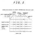
- FIG. 2 is a correlated diagram of growth temperatures and gas flows.
- the material gases are fed into the crystal growth reactor 14 at timings and growth temperatures as shown in FIG. 2.
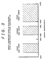
- a growth temperature in crystal growth of InGaN is within a range of from 650°C to 750°C as shown in FIG. 3, while a growth temperature in crystal growth of AlGaN is within a range of from 1000°C to 1200°C as shown in FIGS. 2 and 3.
- InGaN differs remarkably from AlGaN in their growth temperatures in crystal growth. Therefore, it has been heretofore considered that preparation of high quality crystal of InAlGaN is impossible.
- In is 2% to 20%, and A1 is 10% to 90% (It is to be noted that total in ratios of composition of In, Al, and Ga is 100%). In this case, it is preferred that a ratio of composition of In is 6% or higher.
- ultraviolet light-emitting InAlGaN is possible to emit light at room temperature with high efficiency in a short-wavelength region in a deep ultraviolet region of a wavelength of 280 nm to 360 nm. Accordingly, when such ultraviolet light-emitting InAlGaN as described above is used, an ultraviolet light-emitting device emitting light in a wavelength region of a wavelength of 280 nm to 360 nm can be prepared.
- FIGS. 4 through 6 experimental results of ultraviolet light-emitting InAlGaN at room temperature will be described by referring to FIGS. 4 through 6 wherein the ultraviolet light-emitting InAlGaN was prepared at 830°C growth temperature and at 120 nm/hour growth rate in the case where a flow rate of ammonia is 2 L/min, that of trimethylgallium is 3 ⁇ mol/min, that of a trimethylindium adduct is 60 ⁇ mol/min, and that of trimethylaluminum is 0.5 ⁇ mol/min with respect to material gases, besides a flow rate of hydrogen is 100 cc/min, and that of nitrogen is 2 L/min with respect to carrier gases.
- FIG. 4 indicates an effect of introduction of Al into InGaN.
- In is introduced inductively into a crystal as a result of introduction of Al into InGaN.
- the most intensive light emission is achieved in the case when In is 6%, and Al is 16% in a ratio of composition of InGaN.
- FIG. 5 indicates an effect of introduction of In into AlGaN. Light-emitting intensity increases remarkably with increase of a ratio of introduction of In into AlGaN as shown in FIG. 5.
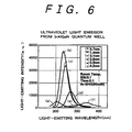
- FIG. 6 indicates results of ultraviolet light emission in the case where an InAlGaN layer having a different ratio of composition is laminated on SiC through an AlGaN buffer layer to form a quantum well structure as shown in FIG. 7, and it is irradiated with laser beam of 257 nm wavelength.
- an ultraviolet light-emitting device such as light-emitting diode, and laser diode provided with a quantum well structure that is prepared by laminating InAlGaN layers having different ratios of composition from one another can be constructed.
- a quantum well structure may be constructed by such a manner that InAlGaN layers formed on SiC through a buffer layer of AlGaN are doped in the form of p-type or n-type, and they are laminated on one another to form the quantum well structure as shown in FIG. 7, thereafter it is provided with electrodes.
- the present invention is constructed as described above, so that it exhibits such an excellent advantage to provide InAlGaN emitting light at room temperature with high efficiency in an ultraviolet short-wavelength region of a wavelength of 360 nm or shorter, and a process for preparing the same as well as an ultraviolet light-emitting device using the InAlGaN emitting light in an ultraviolet short-wavelength region.
Landscapes
- Chemical & Material Sciences (AREA)
- Inorganic Chemistry (AREA)
- Engineering & Computer Science (AREA)
- Materials Engineering (AREA)
- Organic Chemistry (AREA)
- Led Devices (AREA)
- Chemical Vapour Deposition (AREA)
- Luminescent Compositions (AREA)
Abstract
Description
Claims (6)
- InAlGaN emitting light in an ultraviolet short-wavelength region, comprising:
a ratio of composition of In being 2% to 20%, a ratio of composition of Al being 10% to 90%, and a total of ratios of composition of In, Al, and Ga being 100%. - The InAlGaN emitting light in an ultraviolet short-wavelength region as claimed in claim 1 wherein a ratio of composition of In is 6% or more.
- A process for preparing InAlGaN emitting light in an ultraviolet short-wavelength region, comprising:
the InAlGaN being subjected to crystal growth at a growth temperature of 830°C to 950°C in accordance with metalorganic vapor phase epitaxy wherein ammonia, trimethylgallium, a trimethylindium adduct, and trimethylaluminum are used as material gases. - The process for preparing InAlGaN emitting light in an ultraviolet short-wavelength region as claimed in claim 3 wherein a flow rate of the ammonia is 2 L/min, a flow rate of the trimethylgallium is 2 µmol/min to 5 µmol/min, a flow rate of the trimethylindium adduct is 5 µmol/min to 60 µmol/min, and a flow rate of the trimethylaluminum is 0.5 µmol/min to 10 µmol/min.
- An ultraviolet light-emitting device using InAlGaN emitting light in an ultraviolet short-wavelength region, comprising:a first InAlGaN layer wherein a ratio of composition of In is 2% to 20%, a ratio of composition of Al is 10% to 90%, and a total of ratios of composition in In, Al, and Ga is 100%;a second InAlGaN layer ratios of composition of which differ from that of said first layer wherein a ratio of composition of In is 2% to 20%, a ratio of composition of Al is 10% to 90%, and a total of ratios of composition in In, Al, and Ga is 100%; andinvolving a quantum well structure formed by laminating alternately a plurality of layers of said first InAlGaN layer, and said second InAlGaN layer.
- The ultraviolet light-emitting device using InAlGaN emitting light in an ultraviolet short-wavelength region as claimed in claim 5 wherein a ratio of composition of the In in said first InAlGaN layer is 6% or more.
Applications Claiming Priority (2)
| Application Number | Priority Date | Filing Date | Title |
|---|---|---|---|
| JP2000045318A JP3726252B2 (en) | 2000-02-23 | 2000-02-23 | Ultraviolet light emitting device and method for producing InAlGaN light emitting layer |
| JP2000045318 | 2000-02-23 |
Publications (2)
| Publication Number | Publication Date |
|---|---|
| EP1128446A2 true EP1128446A2 (en) | 2001-08-29 |
| EP1128446A3 EP1128446A3 (en) | 2006-06-28 |
Family
ID=18567923
Family Applications (1)
| Application Number | Title | Priority Date | Filing Date |
|---|---|---|---|
| EP01301628A Ceased EP1128446A3 (en) | 2000-02-23 | 2001-02-22 | InAIGaN emitting light in ultraviolet short-wavelenght region and process for preparing the same as well as ultraviolet light-emitting device using the same |
Country Status (5)
| Country | Link |
|---|---|
| US (1) | US7675069B2 (en) |
| EP (1) | EP1128446A3 (en) |
| JP (1) | JP3726252B2 (en) |
| KR (1) | KR100751551B1 (en) |
| CN (2) | CN1264948C (en) |
Cited By (3)
| Publication number | Priority date | Publication date | Assignee | Title |
|---|---|---|---|---|
| EP1551063A4 (en) * | 2002-06-04 | 2006-11-02 | Nitride Semiconductors Co Ltd | GALLIUM NITRIDE SEMICONDUCTOR DEVICE AND METHOD FOR MANUFACTURING THE SAME |
| EP1814164A3 (en) * | 2006-01-26 | 2008-11-05 | Sumitomo Electric Industries, Ltd. | Nitride semiconductor light generating device |
| EP1555697A3 (en) * | 2004-01-14 | 2011-03-09 | Sumitomo Electric Industries, Ltd. | Semiconductor light generating device |
Families Citing this family (13)
| Publication number | Priority date | Publication date | Assignee | Title |
|---|---|---|---|---|
| JP2004356522A (en) * | 2003-05-30 | 2004-12-16 | Sumitomo Chem Co Ltd | Group 3-5 compound semiconductor, its production method and its use |
| JP4110222B2 (en) | 2003-08-20 | 2008-07-02 | 住友電気工業株式会社 | Light emitting diode |
| CN100369198C (en) * | 2004-06-15 | 2008-02-13 | 中国科学院半导体研究所 | Method for preparing crack-free silicon-based III-nitride thin films with self-adaptive flexible layer |
| JP4206086B2 (en) * | 2004-08-03 | 2009-01-07 | 住友電気工業株式会社 | Nitride semiconductor light emitting device and method for manufacturing nitride semiconductor light emitting device |
| US20060267043A1 (en) * | 2005-05-27 | 2006-11-30 | Emerson David T | Deep ultraviolet light emitting devices and methods of fabricating deep ultraviolet light emitting devices |
| CN100437910C (en) * | 2006-07-27 | 2008-11-26 | 中国科学院半导体研究所 | Method of epitaxial InAlGaN single crystal thin film by MBE |
| JP5316210B2 (en) | 2009-05-11 | 2013-10-16 | 住友電気工業株式会社 | Nitride semiconductor light emitting device |
| KR101303031B1 (en) | 2010-05-04 | 2013-09-03 | 조병구 | Method for the formation of multi component thin films and quantum well structure containing multi component by sub-lattice structure controlling technique through Plasma-enhanced atomic layer deposition |
| WO2011152331A1 (en) * | 2010-06-03 | 2011-12-08 | 国立大学法人京都大学 | Ultraviolet irradiation device |
| KR102142714B1 (en) * | 2014-02-18 | 2020-08-07 | 엘지이노텍 주식회사 | Ultraviolet light emitting device and ultraviolet light emitting device package having the same |
| JP6242238B2 (en) * | 2014-02-26 | 2017-12-06 | 学校法人 名城大学 | Method for producing nitride semiconductor multi-element mixed crystal |
| KR102562513B1 (en) * | 2021-03-30 | 2023-08-02 | (주)제니컴 | Graphene nano-structure gas sensor and its fabrication method |
| JP7820180B2 (en) * | 2022-02-14 | 2026-02-25 | ヌヴォトンテクノロジージャパン株式会社 | Nitride-based semiconductor light-emitting device |
Family Cites Families (30)
| Publication number | Priority date | Publication date | Assignee | Title |
|---|---|---|---|---|
| EP0259026B1 (en) * | 1986-08-08 | 1994-04-27 | Kabushiki Kaisha Toshiba | Double-heterostructure semiconductor laser with mesa stripe waveguide |
| JPH0614564B2 (en) * | 1987-07-13 | 1994-02-23 | 日本電信電話株式会社 | Semiconductor light emitting element |
| JPH06101587B2 (en) * | 1989-03-01 | 1994-12-12 | 日本電信電話株式会社 | Semiconductor light emitting element |
| JP3193981B2 (en) | 1990-02-28 | 2001-07-30 | 豊田合成株式会社 | Gallium nitride based compound semiconductor light emitting device |
| JP3026102B2 (en) | 1990-10-27 | 2000-03-27 | 豊田合成株式会社 | Gallium nitride based compound semiconductor light emitting device |
| JP2965709B2 (en) * | 1990-12-07 | 1999-10-18 | 日本電信電話株式会社 | Method for manufacturing semiconductor light emitting device |
| JPH0831419B2 (en) * | 1990-12-25 | 1996-03-27 | 名古屋大学長 | Method for producing compound semiconductor single crystal on single crystal silicon substrate |
| JP3160914B2 (en) * | 1990-12-26 | 2001-04-25 | 豊田合成株式会社 | Gallium nitride based compound semiconductor laser diode |
| JPH0529653A (en) * | 1991-07-19 | 1993-02-05 | Toshiba Corp | Semiconductor element |
| JP3251046B2 (en) * | 1992-03-03 | 2002-01-28 | シャープ株式会社 | Method for growing compound semiconductor, compound semiconductor light emitting device and method for manufacturing the same |
| JP3243768B2 (en) * | 1992-07-06 | 2002-01-07 | 日本電信電話株式会社 | Semiconductor light emitting device |
| JP2681733B2 (en) * | 1992-10-29 | 1997-11-26 | 豊田合成株式会社 | Nitrogen-3 group element compound semiconductor light emitting device |
| JPH06164055A (en) * | 1992-11-25 | 1994-06-10 | Asahi Chem Ind Co Ltd | Quantum well semiconductor laser |
| JP2932467B2 (en) * | 1993-03-12 | 1999-08-09 | 日亜化学工業株式会社 | Gallium nitride based compound semiconductor light emitting device |
| JP2778405B2 (en) * | 1993-03-12 | 1998-07-23 | 日亜化学工業株式会社 | Gallium nitride based compound semiconductor light emitting device |
| JP3243111B2 (en) * | 1993-03-15 | 2002-01-07 | 株式会社東芝 | Compound semiconductor device |
| JP3329573B2 (en) * | 1994-04-18 | 2002-09-30 | 日亜化学工業株式会社 | LED display |
| JPH0818159A (en) * | 1994-04-25 | 1996-01-19 | Hitachi Ltd | Semiconductor laser device and manufacturing method thereof |
| JP3064891B2 (en) * | 1995-02-03 | 2000-07-12 | 住友化学工業株式会社 | Group 3-5 compound semiconductor, method of manufacturing the same, and light emitting device |
| EP0732754B1 (en) * | 1995-03-17 | 2007-10-31 | Toyoda Gosei Co., Ltd. | Light-emitting semiconductor device using group III nitride compound |
| EP0742622A3 (en) * | 1995-03-27 | 1997-02-19 | Mitsubishi Cable Ind Ltd | Laser diode |
| WO1997013303A1 (en) | 1995-09-29 | 1997-04-10 | Matsushita Electric Industrial Co., Ltd. | Semiconductor laser and optical disk device using the laser |
| JPH09153645A (en) | 1995-11-30 | 1997-06-10 | Toyoda Gosei Co Ltd | Group III nitride semiconductor light emitting device |
| US5828684A (en) * | 1995-12-29 | 1998-10-27 | Xerox Corporation | Dual polarization quantum well laser in the 200 to 600 nanometers range |
| JP2927279B2 (en) * | 1996-07-29 | 1999-07-28 | 日亜化学工業株式会社 | Light emitting diode |
| US6020602A (en) | 1996-09-10 | 2000-02-01 | Kabushiki Kaisha Toshba | GaN based optoelectronic device and method for manufacturing the same |
| JP3957359B2 (en) | 1997-05-21 | 2007-08-15 | シャープ株式会社 | Gallium nitride compound semiconductor light emitting device and method for manufacturing the same |
| JPH11340580A (en) | 1997-07-30 | 1999-12-10 | Fujitsu Ltd | Semiconductor laser, semiconductor light emitting device, and method of manufacturing the same |
| JPH11261105A (en) * | 1998-03-11 | 1999-09-24 | Toshiba Corp | Semiconductor light emitting device |
| US6521917B1 (en) * | 1999-03-26 | 2003-02-18 | Matsushita Electric Industrial Co., Ltd. | Semiconductor structures using a group III-nitride quaternary material system with reduced phase separation |
-
2000
- 2000-02-23 JP JP2000045318A patent/JP3726252B2/en not_active Expired - Fee Related
-
2001
- 2001-02-21 KR KR1020010008761A patent/KR100751551B1/en not_active Expired - Fee Related
- 2001-02-22 EP EP01301628A patent/EP1128446A3/en not_active Ceased
- 2001-02-23 CN CNB01112377XA patent/CN1264948C/en not_active Expired - Fee Related
- 2001-02-23 CN CN2005100525886A patent/CN1660962A/en active Pending
- 2001-02-23 US US09/790,660 patent/US7675069B2/en not_active Expired - Fee Related
Cited By (5)
| Publication number | Priority date | Publication date | Assignee | Title |
|---|---|---|---|---|
| EP1551063A4 (en) * | 2002-06-04 | 2006-11-02 | Nitride Semiconductors Co Ltd | GALLIUM NITRIDE SEMICONDUCTOR DEVICE AND METHOD FOR MANUFACTURING THE SAME |
| US7372066B2 (en) | 2002-06-04 | 2008-05-13 | Nitride Semiconductors Co., Ltd. | Gallium nitride compound semiconductor device and manufacturing method |
| EP1555697A3 (en) * | 2004-01-14 | 2011-03-09 | Sumitomo Electric Industries, Ltd. | Semiconductor light generating device |
| EP1814164A3 (en) * | 2006-01-26 | 2008-11-05 | Sumitomo Electric Industries, Ltd. | Nitride semiconductor light generating device |
| US7576351B2 (en) | 2006-01-26 | 2009-08-18 | Sumitomo Electric Industries, Ltd. | Nitride semiconductor light generating device |
Also Published As
| Publication number | Publication date |
|---|---|
| KR100751551B1 (en) | 2007-08-23 |
| US20010028064A1 (en) | 2001-10-11 |
| JP2001237455A (en) | 2001-08-31 |
| KR20010085447A (en) | 2001-09-07 |
| JP3726252B2 (en) | 2005-12-14 |
| CN1264948C (en) | 2006-07-19 |
| US7675069B2 (en) | 2010-03-09 |
| EP1128446A3 (en) | 2006-06-28 |
| CN1311284A (en) | 2001-09-05 |
| CN1660962A (en) | 2005-08-31 |
Similar Documents
| Publication | Publication Date | Title |
|---|---|---|
| US8420426B2 (en) | Method of manufacturing a light-emitting device | |
| US7675069B2 (en) | InAlGaN emitting light in ultraviolet short-wavelength region and process for preparing the same as well as ultraviolet light-emitting device using the same | |
| KR100884288B1 (en) | Nitride semiconductors, light emitting devices using nitride semiconductors, light emitting diodes, laser devices and lamps, and manufacturing methods thereof | |
| JP2007073630A (en) | Semiconductor light emitting device and lighting device using the same | |
| JP2017139252A (en) | Ultraviolet light emitting element | |
| US6445009B1 (en) | Stacking of GaN or GaInN quantum dots on a silicon substrate, their preparation procedure electroluminescent device and lighting device comprising these stackings | |
| TW200832758A (en) | GaN semiconductor light emitting element | |
| JP2012204540A (en) | Semiconductor device and method of manufacturing the same | |
| JP4856666B2 (en) | Light emitting diode element and method for manufacturing the same | |
| JP3605907B2 (en) | Semiconductor device having contact resistance reduction layer | |
| CN111029448A (en) | A kind of near-ultraviolet LED using MOCVD technology and preparation method thereof | |
| JP2006066641A (en) | Semiconductor device and manufacturing method thereof | |
| JPH09186403A (en) | Semiconductor light emitting device and method of manufacturing the same | |
| JP3344189B2 (en) | Semiconductor device having distributed Bragg reflection mirror multilayer film | |
| JP4757976B2 (en) | GaN compound semiconductor manufacturing method | |
| JP3858042B2 (en) | Ultraviolet light emitting device and method for producing InAlGaN light emitting layer | |
| CN104241458A (en) | Method for preparing gallium-nitride-based LED epitaxial wafer with variable barrier width | |
| KR100312019B1 (en) | Fabrication Method for White Light Emitting Diode Using InGaN Phase Separation | |
| JP2001015808A (en) | Nitrogen compound semiconductor light emitting device and method of manufacturing the same | |
| JP2004111865A (en) | Semiconductor substrate and method of manufacturing the same | |
| JPH03252178A (en) | Light emitting element of gallium nitride compound semiconductor | |
| JP2006310886A (en) | Group 3-5 compound semiconductor light emitting device | |
| JP2004048047A (en) | Group 3-5 compound semiconductor light emitting device | |
| Yamabi et al. | Investigation of the Optimum Growth Conditions of Wide-Bandgap Quaternary InAlGaN for UV-LEDs | |
| JP2003179257A (en) | Method for producing gallium nitride-based compound semiconductor containing indium |
Legal Events
| Date | Code | Title | Description |
|---|---|---|---|
| PUAI | Public reference made under article 153(3) epc to a published international application that has entered the european phase |
Free format text: ORIGINAL CODE: 0009012 |
|
| AK | Designated contracting states |
Kind code of ref document: A2 Designated state(s): AT BE CH CY DE DK ES FI FR GB GR IE IT LI LU MC NL PT SE TR |
|
| AX | Request for extension of the european patent |
Free format text: AL;LT;LV;MK;RO;SI |
|
| PUAL | Search report despatched |
Free format text: ORIGINAL CODE: 0009013 |
|
| AK | Designated contracting states |
Kind code of ref document: A3 Designated state(s): AT BE CH CY DE DK ES FI FR GB GR IE IT LI LU MC NL PT SE TR |
|
| AX | Request for extension of the european patent |
Extension state: AL LT LV MK RO SI |
|
| 17P | Request for examination filed |
Effective date: 20061102 |
|
| AKX | Designation fees paid |
Designated state(s): DE FR GB |
|
| 17Q | First examination report despatched |
Effective date: 20070327 |
|
| APBK | Appeal reference recorded |
Free format text: ORIGINAL CODE: EPIDOSNREFNE |
|
| APBN | Date of receipt of notice of appeal recorded |
Free format text: ORIGINAL CODE: EPIDOSNNOA2E |
|
| APBR | Date of receipt of statement of grounds of appeal recorded |
Free format text: ORIGINAL CODE: EPIDOSNNOA3E |
|
| APAV | Appeal reference deleted |
Free format text: ORIGINAL CODE: EPIDOSDREFNE |
|
| APBT | Appeal procedure closed |
Free format text: ORIGINAL CODE: EPIDOSNNOA9E |
|
| STAA | Information on the status of an ep patent application or granted ep patent |
Free format text: STATUS: THE APPLICATION HAS BEEN REFUSED |
|
| 18R | Application refused |
Effective date: 20141205 |