EP1126507A2 - Apparatus for positioning a thin plate - Google Patents
Apparatus for positioning a thin plate Download PDFInfo
- Publication number
- EP1126507A2 EP1126507A2 EP01301033A EP01301033A EP1126507A2 EP 1126507 A2 EP1126507 A2 EP 1126507A2 EP 01301033 A EP01301033 A EP 01301033A EP 01301033 A EP01301033 A EP 01301033A EP 1126507 A2 EP1126507 A2 EP 1126507A2
- Authority
- EP
- European Patent Office
- Prior art keywords
- thin plate
- placement surface
- stage
- semiconductor element
- flat
- Prior art date
- Legal status (The legal status is an assumption and is not a legal conclusion. Google has not performed a legal analysis and makes no representation as to the accuracy of the status listed.)
- Granted
Links
Images


Classifications
-
- H—ELECTRICITY
- H10—SEMICONDUCTOR DEVICES; ELECTRIC SOLID-STATE DEVICES NOT OTHERWISE PROVIDED FOR
- H10P—GENERIC PROCESSES OR APPARATUS FOR THE MANUFACTURE OR TREATMENT OF DEVICES COVERED BY CLASS H10
- H10P72/00—Handling or holding of wafers, substrates or devices during manufacture or treatment thereof
- H10P72/50—Handling or holding of wafers, substrates or devices during manufacture or treatment thereof for positioning, orientation or alignment
- H10P72/53—Handling or holding of wafers, substrates or devices during manufacture or treatment thereof for positioning, orientation or alignment using optical controlling means
-
- H—ELECTRICITY
- H10—SEMICONDUCTOR DEVICES; ELECTRIC SOLID-STATE DEVICES NOT OTHERWISE PROVIDED FOR
- H10W—GENERIC PACKAGES, INTERCONNECTIONS, CONNECTORS OR OTHER CONSTRUCTIONAL DETAILS OF DEVICES COVERED BY CLASS H10
- H10W72/00—Interconnections or connectors in packages
- H10W72/071—Connecting or disconnecting
- H10W72/0711—Apparatus therefor
-
- H—ELECTRICITY
- H10—SEMICONDUCTOR DEVICES; ELECTRIC SOLID-STATE DEVICES NOT OTHERWISE PROVIDED FOR
- H10W—GENERIC PACKAGES, INTERCONNECTIONS, CONNECTORS OR OTHER CONSTRUCTIONAL DETAILS OF DEVICES COVERED BY CLASS H10
- H10W72/00—Interconnections or connectors in packages
- H10W72/071—Connecting or disconnecting
- H10W72/0711—Apparatus therefor
- H10W72/07178—Means for aligning
-
- H—ELECTRICITY
- H10—SEMICONDUCTOR DEVICES; ELECTRIC SOLID-STATE DEVICES NOT OTHERWISE PROVIDED FOR
- H10W—GENERIC PACKAGES, INTERCONNECTIONS, CONNECTORS OR OTHER CONSTRUCTIONAL DETAILS OF DEVICES COVERED BY CLASS H10
- H10W72/00—Interconnections or connectors in packages
- H10W72/071—Connecting or disconnecting
- H10W72/075—Connecting or disconnecting of bond wires
-
- H—ELECTRICITY
- H10—SEMICONDUCTOR DEVICES; ELECTRIC SOLID-STATE DEVICES NOT OTHERWISE PROVIDED FOR
- H10W—GENERIC PACKAGES, INTERCONNECTIONS, CONNECTORS OR OTHER CONSTRUCTIONAL DETAILS OF DEVICES COVERED BY CLASS H10
- H10W72/00—Interconnections or connectors in packages
- H10W72/50—Bond wires
- H10W72/551—Materials of bond wires
- H10W72/552—Materials of bond wires comprising metals or metalloids, e.g. silver
- H10W72/5522—Materials of bond wires comprising metals or metalloids, e.g. silver comprising gold [Au]
-
- H—ELECTRICITY
- H10—SEMICONDUCTOR DEVICES; ELECTRIC SOLID-STATE DEVICES NOT OTHERWISE PROVIDED FOR
- H10W—GENERIC PACKAGES, INTERCONNECTIONS, CONNECTORS OR OTHER CONSTRUCTIONAL DETAILS OF DEVICES COVERED BY CLASS H10
- H10W72/00—Interconnections or connectors in packages
- H10W72/90—Bond pads, in general
- H10W72/951—Materials of bond pads
Definitions
- the present invention relates to an apparatus for positioning a thin plate and, more specifically, to an apparatus for detecting a mark provided at a predetermined position on a thin plate placed on a stage and positioning the thin plate in place.
- a flip-chip system can be adopted wherein electrode terminals of a semiconductor element are directly placed on a circuit board for forming a semiconductor device package.
- Fig. 5 One method for forming such bumps is illustrated in Fig. 5.
- a semiconductor element 10 has been placed on a table 200 adapted to be movable in the horizontal direction so that electrode terminals 12 thereof are directed upward (see Fig. 5(a))
- a gold bump 14 having a pointed distal end is formed on the respective electrode terminal 12, 12, ⁇ (see Fig. 5(b)).
- This gold bump 14 is formed on the electrode terminal 12 by using a bonding device 40 shown in Fig. 6.
- a tip end of a gold wire 44 wound on a wire spool 42 is heated, after passing through a clamper 46 and a capillary 48, to form a ball-like end 49. Thereafter, the capillary 48 descends to pressingly bond the ball-like end 49 onto the electrode terminal 12. Then, the gold wire 44 is stretchingly severed by means of the clamper 46 to form the gold bump 14 having a pointed tip end.
- Such gold bumps 14, 14, ⁇ having the pointed ends are then subjected to a flattening treatment to be converted into bumps 16, 16, ⁇ having flat ends (see Fig. 5(c)).
- the semiconductor element 10 placed on the table 200 is initially detected and located (fixed) at a predetermined position since it is necessary to form the ball-like ends 49 of the gold wire 44 exactly above the electrode terminals 12, 12, ⁇ of the semiconductor element 10.
- the electrode terminals 12, 12, ⁇ of the semiconductor element 10 detected and located on the table 200 are formed at predetermined positions on one surface of the semiconductor element 10.
- the semiconductor element 10 is movable by, for example, a controller (not shown) for controlling a drive means such as a servo-motor (not shown) for moving the table 200 in the horizontal direction so that a selected electrode terminal 12 on which the gold bump 14 is to be formed is positioned exactly beneath the ball-like end 49 of the gold wire 44.
- the detection and positioning of the semiconductor element 10 placed on the table 200 are carried out by a positioning device shown in Fig. 7.
- the positioning device shown in Fig. 7 includes the table 200 movable in the horizontal direction and having a suction hole 204 formed in a central region of the table 200 and fluidly connected to a vacuum generating means 202 such as a vacuum pump, four pusher members 100 provided so that a front end face of each thereof abuts to the respective side of the rectangular semiconductor element 10 and is movable to be away from and closer to the semiconductor element 10 to slide the semiconductor element 10 in the predetermined direction, a camera 50 such as a CCD for detecting marks provided at a selected position on the surface of the semiconductor element 10 placed on the table 200, and an optical detection means having a controller 52 for controlling a drive means (not shown) such as a servo-motor for moving the camera 50 leftward and rightward.
- a vacuum generating means 202 such as a vacuum pump
- four pusher members 100 provided so that a front end face of each thereof abuts to the respective side of the rectangular semiconductor element 10 and is movable to be away from and closer to the semiconductor element
- the camera 50 has a high magnification to accurately detect the marks formed on one surface of the semiconductor element 10, which means that the camera 50 has a smaller field of view 54. Accordingly, as shown in Fig. 7, it is impossible to cover all of one surface of the semiconductor element 10 by the field of view 54 of the camera 50 but only part of the semiconductor element 10 can be covered.
- the respective pusher members 100 move to cause the front end faces thereof to abut to the four sides of the rectangular semiconductor element 10, respectively, in four directions, to slide the semiconductor element 10 on the table 200 so that the mark 18 of the semiconductor element 10 is within the field of view 54 of the camera 50 located at a fixed position, as shown in Fig. 8(b).
- the position of the semiconductor element 10 is easily detectable.
- the vacuum generating means 202 such as a vacuum pump is driven to secure the semiconductor element 10 thus detected on the table 200 through the suction hole 204, after which the table moves to the subsequent process.
- the front end faces of the pusher members 100 abut to sides of the semiconductor element 10, respectively, to slide the latter, as shown in Figs. 7 and 8(b). Therefore, a pushing force applied to the semiconductor element 10 by the two pusher members 100 opposite to each other is liable to bend the semiconductor element 10.
- the semiconductor element 10 has been made thinner; for example, in an extreme case, a thickness is less than 150 ⁇ m.
- a thickness is less than 150 ⁇ m.
- Such a thin semiconductor element 10 may be bent due to a pushing force applied thereto while gripping the same between the front end faces of pusher members 100 disposed opposite to each other. In the semiconductor element 10 thus bent, even though the mark 18 is caught within the field of view of the camera 50, the position of the mark cannot be correctly detected.
- stopper portions are provided at opposite corners of a positioning stage, and position-restricting surfaces corresponding to outer sides of leads of a workpiece and contact surfaces to abut to the stopper portions are provided in pusher members, wherein the positional relationship between the position-restricting surfaces, the stopper portions and the contact surfaces is so selected that a sum of gaps between the position-restricting surfaces and the outer sides of the leads of the workpiece is equal to a predetermined value when the pusher members reach their foremost positions.
- a die-bonding device wherein a semiconductor chip is located on a positioning stage by a positioning member, then moves to a bonding position on a body to be bonded by means of a bonding head and is bonded onto the body.
- a protrusion is formed in a central region of the positioning stage, having a size smaller than the semiconductor chip. According to this device, any debris generated from the semiconductor chip during the positioning operation is not left on the stage surface on which the positioning of the semiconductor is carried out, whereby the positioning member can assuredly be brought into contact with the semiconductor chip every time to accurately locate the latter at a predetermined position.
- an object of the present invention is to provide an apparatus for positioning a thin plate placed on a table, by slide means such as pusher members, which is free from a risk of bending the thin plate due to a pushing force applied thereto by the slide means while gripping the thin plate between front end faces of the slide means.
- the inventors have studied to solve the above-mentioned problem in the prior art and found that it is possible to adjust a position of a thin plate without applying a large pushing force which can bend the thin plate by a slide means, by forming a stage on a table for placing the thin plate such as a semiconductor element.
- the stage has a flat placement surface for placing the thin plate thereon having such an area that when the thin plate is placed on the placement surface without projecting out therefrom, a mark formed on one surface of the thin plate is always caught within a field of view of a camera.
- the slide means is adapted to sliding the thin sheet placed on the placement surface of the stage to move the projected part of the thin plate into the area of the placement surface, so that a front end face of the slide means abuts to a lateral side of the stage.
- an apparatus for positioning a thin plate comprising: a stage having a flat placement surface on which said thin plate is mounted, said placement surface having a flat region which is slightly larger than, and completely covers, said thin plate, said placement surface also having at least one lateral side edge; optical detecting means arranged above said stage for detecting a mark provided on said thin plate, said optical detecting means having such a view that said mark can be caught by said view if said thin plate placed on said placement surface is within said flat region of the placement surface, but said mark cannot be caught by said view if said thin plate placed on said placement surface protrudes by a part thereof from said flat region of the placement surface; and adjusting means having a movable part which pushes said thin plate until it comes into contact with said lateral edge to move said thin plate so that said thin plate is brought within said flat region of the placement surface.
- the flat placement surface is an upwardly protruded portion from a lower flat surface of a table and said movable part of the adjusting means is a pusher member which slidingly moves on said lower flat surface.
- the thin plate slide means includes a pusher member having a front end face movable to be in contact with or move away from the lateral side of the stage on the table, the slide means becomes simple in structure.
- the means for fixing the thin plate at a predetermined position has a plurality of suction holes opened on the placement surface, the thin plate can be sucked by a plurality of positions whereby the deformation thereof is avoidable.
- the present invention is suitably applicable to a semiconductor element 150 ⁇ m thick or less.
- the apparatus for positioning the thin plate of the present invention since the placement surface of the stage is flat and larger than the thin plate, there is no risk in that the thin plate is fixed between the front end faces of the slide means when the projected part of the thin plate placed on the placement surface of the stage formed on one side of the table slides into the area of the placement surface, whereby the bending of the thin plate due to the pushing force is avoidable.
- the placement surface has such an area that when the thin plate is placed on the placement surface without projecting outside thereof, the mark on the thin plate is always caught in the field of view of the camera.
- the mark is also within the field of view of the camera, whereby the position of the thin plate is easily detectable.
- the thin plate thus position-detected is fixed on the stage by the fixing means to complete the positioning operation.
- An apparatus for positioning a thin plate such as a semiconductor element shown in Figs. 1 and 2, includes a table 20 movable in the horizontal direction.
- a stage 22 having a rectangular placement surface 22a is formed in a protruded state for placing a semiconductor element 10 thereon.
- the flat placement surface 22a is higher by a dimension "t" from the upper surface 20a of the table 20.
- a plurality of suction holes 24 are open on the placement surface of the stage 22 and coupled to a vacuum generating means 26 such as a vacuum pump.
- Pusher members 30 are provided at the respective lateral sides of the stage 22 so that front end faces thereof are slidingly moved on the upper surface 20a of the table 20 to be in contact with and away from the lateral sides of the stage 22, respectively.
- An upper portion of the front end face of the pusher member 30 is formed to be higher by a dimension "a" than the placement surface of the stage 22 so that it abuts to a projected part of the semiconductor element 10 to slide the semiconductor element 10 along and into the placement surface 22a.
- a camera 50 such as a CCD camera, for detecting marks formed at predetermined positions on an upper side of the semiconductor element 10 placed on the placement surface 22a, which constitutes an optical detection means in association with a controller 52 for controlling means (not shown) for driving the camera 50 to move leftward and rightward.
- the placement surface 22a of the stage 22 shown in Fig. 1 is flat and formed to be slightly broader than the semiconductor element 10 placed thereon, and completely covers the flat region of the semiconductor element 10.
- the placement surface 22a has such an area that the marks formed on the one side of the semiconductor element 10 are always present within the field of view of the camera 50 when the semiconductor element 10 is placed on the placement surface 22a without being projected outside thereof.
- the mark formed on the one side of the semiconductor element 10 can be positioned within the field of view 54 of the camera 50.
- the width of the front end face of the respective pusher member 30 is substantially the same or a little smaller than the length of the corresponding lateral side of the stage 22.
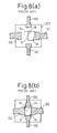
- Figs. 3(a) and 3(b) The operation will be illustrated, in Figs. 3(a) and 3(b), for sliding the semiconductor element 10 by the pusher members 30 to move the projected part of the semiconductor element toward the stage 22 to be correctly placed thereon.
- Fig. 3(a) if the semiconductor element 10 is placed on the stage 22 with part thereof projected from the placement surface, the marks 18 of the semiconductor element 10 are out of the field of view 54 of the camera 50.
- the four pusher members 30 arranged to encircle the stage 22 are driven to slidingly move on the upper surface 20a of the table 20 toward the stage 22, whereby the projected part of the semiconductor element 10 moves onto the placement surface 22a by the contact of the front end face of the pusher member 30 in contact therewith.
- the slide motion of the semiconductor element 10 has completed, and the semiconductor element 10 is placed on the placement surface of the stage 22 without being projected out thereof as shown in Fig. 3(b).
- one of the marks 18 formed on the semiconductor element 10 is within the field of view 54 of the camera 50.
- the area of the placement surface 22a of the stage 22 is formed slightly broader than that of the semiconductor element 10 so that one of the marks 18 formed on one side of the semiconductor element is always within the field of view 54 of the camera 50.
- the placement surface 22a of the semiconductor element 10 is formed broader than the semiconductor element 10, no force is applied from the pusher member 30 to the semiconductor element 10 correctly placed on the placement surface 22a of the stage 22 without being projected out thereof.
- the semiconductor element 10 Since the semiconductor element 10 is placed on the placement surface of the stage 22 protruded upward from the table 20, there is no risk in that the semiconductor element 10 enters into a gap 28 (see Fig. 1) between the table 20 and the pusher member 30 even if the semiconductor element 10 is as thin as 150 ⁇ m or less or, particularly, 100 ⁇ m or less.
- the position of the semiconductor element 10 is determined by detecting the positions of the marks 18. Since the positions of the marks 18 are preliminarily known, if one of them is detected, the other is easily detectable.
- the vacuum generating means 26 such as a vacuum pump is driven to evacuate the plurality of suction holes 24 so that the semiconductor element 10 is fixed to the placement surface 22a of the stage 22.
- the semiconductor element 10 suckingly fixed to the placement surface of the stage 22 is moved together with the table 20 while fixed to the stage 22 to a subsequent process such as that for the formation of bumps by a bonding device 40 shown in Fig. 6.
- a pair of L-shaped pusher members 32 may be provided to be in contact with and away from the respective sides of the stage 22 as shown in Fig. 4.
- the apparatus for positioning a thin plate it is possible to position the thin plate while preventing it from entering a gap between a table and a slide means or from bending by the operation of the slide means, so that the position of the thin plate is easily detectable by an optical detection device.
- the thin plate fixed onto the table by the fixing means is quickly movable to a subsequent process to be subjected to a desired treatment.
Landscapes
- Container, Conveyance, Adherence, Positioning, Of Wafer (AREA)
Abstract
Description
Claims (6)
- An apparatus for positioning a thin plate comprising:a stage having a flat placement surface on which said thin plate is mounted, said placement surface having a flat region which is slightly larger than and completely covers that of said thin plate, said placement surface also having at least one lateral side edge;optical detecting means arranged above said stage for detecting a mark provided on said thin plate, said optical detecting means having such a view that said mark can be caught by said view if said thin plate placed on said placement surface is within said flat region of the placement surface, but said mark cannot be caught by said view if said thin plate placed on said placement surface protrudes by a part thereof from said flat region of the placement surface; andadjusting means having a movable part which pushes said thin plate until it comes into contact with said lateral edge to move said thin plate so that said thin plate is brought within said flat region of the placement surface.
- An apparatus as set forth in claim 1, wherein said stage has said flat placement surface which is an upwardly protruded portion from a lower flat surface of a table, and said movable part of the adjusting means is a pusher member which slidingly moves on said lower flat surface.
- An apparatus as set forth in claim 2, wherein said placement surface of the stage has a rectangular shape and has four lateral side edges, and said adjusting means has four pusher members which slidingly move on said lower flat surface until they come into contact with said respective lateral sides of the stage to move said thin plate so that said thin plate is brought within said flat region of the placement surface.
- An apparatus as set forth in claim 3, wherein said pusher members comprises a pair of L-shaped pusher members which slidingly move on said lower flat surface until they come into contact with the adjacent lateral sides of the state.
- An apparatus as set forth in any preceding claim, further comprising a holding means for fixedly holding said thin plate at position on said placement surface, said holding means comprising a plurality of holes provided on said flat placement surface of the stage connected to vacuum suction means.
- An apparatus as set forth in any preceding claim, wherein said thin plate is a semiconductor element having a thickness of not more than 150 µm.
Applications Claiming Priority (2)
| Application Number | Priority Date | Filing Date | Title |
|---|---|---|---|
| JP2000034406 | 2000-02-14 | ||
| JP2000034406A JP3796089B2 (en) | 2000-02-14 | 2000-02-14 | Thin plate positioning device |
Publications (3)
| Publication Number | Publication Date |
|---|---|
| EP1126507A2 true EP1126507A2 (en) | 2001-08-22 |
| EP1126507A3 EP1126507A3 (en) | 2002-07-24 |
| EP1126507B1 EP1126507B1 (en) | 2006-04-19 |
Family
ID=18558759
Family Applications (1)
| Application Number | Title | Priority Date | Filing Date |
|---|---|---|---|
| EP01301033A Expired - Lifetime EP1126507B1 (en) | 2000-02-14 | 2001-02-06 | Apparatus for positioning a thin plate |
Country Status (4)
| Country | Link |
|---|---|
| US (1) | US6354480B2 (en) |
| EP (1) | EP1126507B1 (en) |
| JP (1) | JP3796089B2 (en) |
| DE (1) | DE60118819T2 (en) |
Cited By (2)
| Publication number | Priority date | Publication date | Assignee | Title |
|---|---|---|---|---|
| DE102008045257A1 (en) * | 2008-09-01 | 2010-03-04 | Rena Gmbh | Apparatus and method for handling substrates |
| WO2019057469A1 (en) * | 2017-09-21 | 2019-03-28 | Muehlbauer GmbH & Co. KG | Device for aligning and optically inspecting a semiconductor component |
Families Citing this family (18)
| Publication number | Priority date | Publication date | Assignee | Title |
|---|---|---|---|---|
| US6820792B2 (en) * | 1998-09-30 | 2004-11-23 | Samsung Electronics Co., Ltd. | Die bonding equipment |
| JP3796089B2 (en) * | 2000-02-14 | 2006-07-12 | 新光電気工業株式会社 | Thin plate positioning device |
| US7726540B2 (en) * | 2005-12-12 | 2010-06-01 | Asm Assembly Automation Ltd. | Apparatus and method for arranging devices for processing |
| ATE450359T1 (en) * | 2007-11-20 | 2009-12-15 | Leister Process Tech | METHOD AND AUTOMATIC WELDING MACHINES FOR CONNECTING MATERIAL LINES |
| US20140076956A1 (en) * | 2012-09-20 | 2014-03-20 | Tyco Electronics Corporation | Soldering machine and method of soldering |
| KR20140120641A (en) * | 2013-04-04 | 2014-10-14 | 삼성디스플레이 주식회사 | Film align device |
| US9227261B2 (en) * | 2013-08-06 | 2016-01-05 | Globalfoundries Inc. | Vacuum carriers for substrate bonding |
| WO2015068219A1 (en) * | 2013-11-06 | 2015-05-14 | 東芝三菱電機産業システム株式会社 | Electrode bonding device and electrode bonding method |
| US9510460B2 (en) * | 2014-09-17 | 2016-11-29 | Asm Technology Singapore Pte Ltd | Method for aligning electronic components |
| DE102015106265A1 (en) | 2015-02-06 | 2016-08-11 | Auto-Kabel Management Gmbh | Ultrasonic welding device and method for ultrasonic welding |
| CN106271299A (en) * | 2015-06-03 | 2017-01-04 | 中兴通讯股份有限公司 | The apparatus for welding and positioning of a kind of radio-frequency power amplifier and method |
| EP3373325A4 (en) * | 2015-11-05 | 2019-05-01 | Furukawa Electric Co. Ltd. | CHIP BONDING DEVICE AND CHIP BONDING METHOD |
| CN107378368A (en) * | 2017-08-10 | 2017-11-24 | 东莞市先行者智能设备科技有限公司 | A kind of parallel duplexing bit flipping displacement component and automatic soldering device |
| WO2021202211A1 (en) * | 2020-03-29 | 2021-10-07 | Kulicke And Soffa Industries, Inc. | Methods of optimizing clamping of a semiconductor element against a support structure on a wire bonding machine, and related methods |
| US11540399B1 (en) * | 2020-04-09 | 2022-12-27 | Hrl Laboratories, Llc | System and method for bonding a cable to a substrate using a die bonder |
| CN113539920B (en) * | 2021-07-19 | 2024-04-26 | 天航长鹰(江苏)科技有限公司 | A positioning device for semiconductor chip detection |
| CN116690089B (en) * | 2023-07-03 | 2026-04-17 | 苏州思萃声光微纳技术研究所有限公司 | A visual positioning system and method for bipolar plate welding |
| CN119927405A (en) * | 2023-11-06 | 2025-05-06 | 泰科电子(上海)有限公司 | Welding equipment |
Family Cites Families (17)
| Publication number | Priority date | Publication date | Assignee | Title |
|---|---|---|---|---|
| JPS57194530A (en) * | 1981-05-27 | 1982-11-30 | Oki Electric Ind Co Ltd | Positioning of photomask substrate |
| GB8406129D0 (en) * | 1984-03-08 | 1984-04-11 | Dyna Pert Precima Ltd | Orienting electrical components |
| JP2627296B2 (en) | 1987-03-02 | 1997-07-02 | 日本クラウンコルク株式会社 | Container lid with automatic opening and closing mechanism |
| JPH03206636A (en) * | 1990-01-08 | 1991-09-10 | Nec Corp | Bonding apparatus |
| JPH0474443A (en) | 1990-07-16 | 1992-03-09 | Mitsubishi Electric Corp | Die bonding apparatus and die bonding method using the same |
| JPH04350950A (en) * | 1991-05-28 | 1992-12-04 | Matsushita Electric Ind Co Ltd | Chip positioner |
| US5242103A (en) * | 1992-12-07 | 1993-09-07 | Motorola, Inc. | Pivotal wire bonding stage and method of use |
| US6246204B1 (en) * | 1994-06-27 | 2001-06-12 | Nikon Corporation | Electromagnetic alignment and scanning apparatus |
| JPH10107122A (en) * | 1996-10-01 | 1998-04-24 | Tokyo Electron Ltd | Loading device for substrate cassette to be processed |
| US6129259A (en) * | 1997-03-31 | 2000-10-10 | Micron Technology, Inc. | Bonding and inspection system |
| US5982132A (en) * | 1997-10-09 | 1999-11-09 | Electroglas, Inc. | Rotary wafer positioning system and method |
| JPH11204622A (en) * | 1998-01-07 | 1999-07-30 | Canon Inc | Positioning apparatus and method |
| JP3328190B2 (en) * | 1998-06-08 | 2002-09-24 | ノーゼルエンジニアリング株式会社 | Inspection object positioning apparatus and inspection object positioning method |
| US6213376B1 (en) * | 1998-06-17 | 2001-04-10 | International Business Machines Corp. | Stacked chip process carrier |
| US6085967A (en) * | 1998-12-28 | 2000-07-11 | Eastman Kodak Company | Method of registrably aligning fabricated wafers preceding bonding |
| US6275742B1 (en) * | 1999-04-16 | 2001-08-14 | Berkeley Process Control, Inc. | Wafer aligner system |
| JP3796089B2 (en) * | 2000-02-14 | 2006-07-12 | 新光電気工業株式会社 | Thin plate positioning device |
-
2000
- 2000-02-14 JP JP2000034406A patent/JP3796089B2/en not_active Expired - Fee Related
-
2001
- 2001-02-05 US US09/778,119 patent/US6354480B2/en not_active Expired - Fee Related
- 2001-02-06 DE DE60118819T patent/DE60118819T2/en not_active Expired - Lifetime
- 2001-02-06 EP EP01301033A patent/EP1126507B1/en not_active Expired - Lifetime
Cited By (3)
| Publication number | Priority date | Publication date | Assignee | Title |
|---|---|---|---|---|
| DE102008045257A1 (en) * | 2008-09-01 | 2010-03-04 | Rena Gmbh | Apparatus and method for handling substrates |
| WO2019057469A1 (en) * | 2017-09-21 | 2019-03-28 | Muehlbauer GmbH & Co. KG | Device for aligning and optically inspecting a semiconductor component |
| US11152243B2 (en) | 2017-09-21 | 2021-10-19 | Muehlbauer GmbH & Co. KG | Device for aligning and optically inspecting a semiconductor component |
Also Published As
| Publication number | Publication date |
|---|---|
| DE60118819T2 (en) | 2006-09-21 |
| DE60118819D1 (en) | 2006-05-24 |
| EP1126507B1 (en) | 2006-04-19 |
| US6354480B2 (en) | 2002-03-12 |
| EP1126507A3 (en) | 2002-07-24 |
| US20010013532A1 (en) | 2001-08-16 |
| JP3796089B2 (en) | 2006-07-12 |
| JP2001223255A (en) | 2001-08-17 |
Similar Documents
| Publication | Publication Date | Title |
|---|---|---|
| EP1126507B1 (en) | Apparatus for positioning a thin plate | |
| US20030046812A1 (en) | Chip-mounting device and method of alignment thereof | |
| JPH10261673A (en) | Semiconductor integrated circuit device manufacturing method and bonding device used therefor | |
| JP4831091B2 (en) | Die bonding apparatus and die bonding method | |
| JP2002198398A (en) | Bonding equipment | |
| CN114026677A (en) | Conveying device | |
| JPH05208390A (en) | Suction nozzle | |
| US20020125303A1 (en) | Bonding method and apparatus | |
| JP3617483B2 (en) | Electronic component mounting method | |
| KR20050045828A (en) | Apparatus for mounting semiconductor chips | |
| JPH104095A (en) | Bump bonding apparatus and method | |
| JP3102241B2 (en) | Electronic component bonding apparatus and bonding method | |
| KR0167457B1 (en) | Wire bonding apparatus | |
| JP2746989B2 (en) | Chip positioning method and device, inner lead bonding apparatus, and inner lead bonding method | |
| JP4316122B2 (en) | IC chip setting device | |
| JP4128321B2 (en) | Bump bonding equipment | |
| JP3622727B2 (en) | Ultrasonic bonding apparatus and ultrasonic bonding method | |
| TW202531832A (en) | Bonding systems, and methods of bonding a semiconductor element to a substrate | |
| JP2842852B2 (en) | Method for bonding inner leads for TAB | |
| JP2949872B2 (en) | Electronic component bonding equipment | |
| JP2022112206A (en) | Bonding method and method for using bonding device | |
| JP2000124233A (en) | Die bonding collet and die bonding method using the same | |
| JP3347025B2 (en) | Bump bonding apparatus and method | |
| KR20080080898A (en) | Bump bonding device | |
| JP2003142507A (en) | Semiconductor device manufacturing apparatus and semiconductor device manufacturing method using the same |
Legal Events
| Date | Code | Title | Description |
|---|---|---|---|
| PUAI | Public reference made under article 153(3) epc to a published international application that has entered the european phase |
Free format text: ORIGINAL CODE: 0009012 |
|
| AK | Designated contracting states |
Kind code of ref document: A2 Designated state(s): AT BE CH CY DE DK ES FI FR GB GR IE IT LI LU MC NL PT SE TR |
|
| AX | Request for extension of the european patent |
Free format text: AL;LT;LV;MK;RO;SI |
|
| PUAL | Search report despatched |
Free format text: ORIGINAL CODE: 0009013 |
|
| AK | Designated contracting states |
Kind code of ref document: A3 Designated state(s): AT BE CH CY DE DK ES FI FR GB GR IE IT LI LU MC NL PT SE TR |
|
| AX | Request for extension of the european patent |
Free format text: AL;LT;LV;MK;RO;SI |
|
| 17P | Request for examination filed |
Effective date: 20030108 |
|
| AKX | Designation fees paid |
Designated state(s): DE |
|
| 17Q | First examination report despatched |
Effective date: 20050323 |
|
| GRAP | Despatch of communication of intention to grant a patent |
Free format text: ORIGINAL CODE: EPIDOSNIGR1 |
|
| GRAS | Grant fee paid |
Free format text: ORIGINAL CODE: EPIDOSNIGR3 |
|
| GRAA | (expected) grant |
Free format text: ORIGINAL CODE: 0009210 |
|
| AK | Designated contracting states |
Kind code of ref document: B1 Designated state(s): DE |
|
| REF | Corresponds to: |
Ref document number: 60118819 Country of ref document: DE Date of ref document: 20060524 Kind code of ref document: P |
|
| PLBE | No opposition filed within time limit |
Free format text: ORIGINAL CODE: 0009261 |
|
| STAA | Information on the status of an ep patent application or granted ep patent |
Free format text: STATUS: NO OPPOSITION FILED WITHIN TIME LIMIT |
|
| 26N | No opposition filed |
Effective date: 20070122 |
|
| PGFP | Annual fee paid to national office [announced via postgrant information from national office to epo] |
Ref country code: DE Payment date: 20120131 Year of fee payment: 12 |
|
| REG | Reference to a national code |
Ref country code: DE Ref legal event code: R119 Ref document number: 60118819 Country of ref document: DE Effective date: 20130903 |
|
| PG25 | Lapsed in a contracting state [announced via postgrant information from national office to epo] |
Ref country code: DE Free format text: LAPSE BECAUSE OF NON-PAYMENT OF DUE FEES Effective date: 20130903 |