EP1124666B1 - Use of zeta potential during chemical mechanical polishing for end point detection - Google Patents
Use of zeta potential during chemical mechanical polishing for end point detection Download PDFInfo
- Publication number
- EP1124666B1 EP1124666B1 EP99950284A EP99950284A EP1124666B1 EP 1124666 B1 EP1124666 B1 EP 1124666B1 EP 99950284 A EP99950284 A EP 99950284A EP 99950284 A EP99950284 A EP 99950284A EP 1124666 B1 EP1124666 B1 EP 1124666B1
- Authority
- EP
- European Patent Office
- Prior art keywords
- polishing
- fluid
- zeta potential
- pad
- change
- Prior art date
- Legal status (The legal status is an assumption and is not a legal conclusion. Google has not performed a legal analysis and makes no representation as to the accuracy of the status listed.)
- Expired - Lifetime
Links
- 238000005498 polishing Methods 0.000 title claims abstract description 115
- 238000001514 detection method Methods 0.000 title description 19
- 239000000126 substance Substances 0.000 title description 7
- 239000012530 fluid Substances 0.000 claims abstract description 150
- 239000000463 material Substances 0.000 claims abstract description 100
- 230000008859 change Effects 0.000 claims abstract description 66
- 238000000034 method Methods 0.000 claims abstract description 59
- 239000002002 slurry Substances 0.000 claims abstract description 54
- 239000004065 semiconductor Substances 0.000 claims abstract description 21
- 239000000758 substrate Substances 0.000 claims description 27
- 239000007788 liquid Substances 0.000 claims description 6
- 230000007704 transition Effects 0.000 abstract description 3
- 235000012431 wafers Nutrition 0.000 description 61
- 229910052581 Si3N4 Inorganic materials 0.000 description 36
- 239000002245 particle Substances 0.000 description 29
- 239000010949 copper Substances 0.000 description 22
- 230000008569 process Effects 0.000 description 20
- 239000010408 film Substances 0.000 description 18
- 229910052751 metal Inorganic materials 0.000 description 16
- 239000002184 metal Substances 0.000 description 16
- 229910052802 copper Inorganic materials 0.000 description 15
- RYGMFSIKBFXOCR-UHFFFAOYSA-N Copper Chemical compound [Cu] RYGMFSIKBFXOCR-UHFFFAOYSA-N 0.000 description 13
- VYPSYNLAJGMNEJ-UHFFFAOYSA-N Silicium dioxide Chemical compound O=[Si]=O VYPSYNLAJGMNEJ-UHFFFAOYSA-N 0.000 description 12
- 230000004888 barrier function Effects 0.000 description 12
- 230000009977 dual effect Effects 0.000 description 10
- 238000012544 monitoring process Methods 0.000 description 10
- 238000004519 manufacturing process Methods 0.000 description 9
- 230000004044 response Effects 0.000 description 9
- 238000007517 polishing process Methods 0.000 description 8
- XUIMIQQOPSSXEZ-UHFFFAOYSA-N Silicon Chemical compound [Si] XUIMIQQOPSSXEZ-UHFFFAOYSA-N 0.000 description 7
- 229910052710 silicon Inorganic materials 0.000 description 7
- 239000010703 silicon Substances 0.000 description 7
- 239000000377 silicon dioxide Substances 0.000 description 6
- 230000007423 decrease Effects 0.000 description 4
- 230000000694 effects Effects 0.000 description 4
- 235000012239 silicon dioxide Nutrition 0.000 description 4
- 230000015572 biosynthetic process Effects 0.000 description 3
- 239000007789 gas Substances 0.000 description 3
- 238000012545 processing Methods 0.000 description 3
- 239000000725 suspension Substances 0.000 description 3
- 238000012876 topography Methods 0.000 description 3
- IJGRMHOSHXDMSA-UHFFFAOYSA-N Atomic nitrogen Chemical compound N#N IJGRMHOSHXDMSA-UHFFFAOYSA-N 0.000 description 2
- 238000012935 Averaging Methods 0.000 description 2
- ATJFFYVFTNAWJD-UHFFFAOYSA-N Tin Chemical compound [Sn] ATJFFYVFTNAWJD-UHFFFAOYSA-N 0.000 description 2
- 229910052782 aluminium Inorganic materials 0.000 description 2
- XAGFODPZIPBFFR-UHFFFAOYSA-N aluminium Chemical compound [Al] XAGFODPZIPBFFR-UHFFFAOYSA-N 0.000 description 2
- 238000013459 approach Methods 0.000 description 2
- 239000000084 colloidal system Substances 0.000 description 2
- 150000001875 compounds Chemical class 0.000 description 2
- 230000001419 dependent effect Effects 0.000 description 2
- 238000013461 design Methods 0.000 description 2
- 238000005516 engineering process Methods 0.000 description 2
- 239000011521 glass Substances 0.000 description 2
- 238000011065 in-situ storage Methods 0.000 description 2
- 230000007246 mechanism Effects 0.000 description 2
- 239000007769 metal material Substances 0.000 description 2
- 150000002739 metals Chemical class 0.000 description 2
- 150000004767 nitrides Chemical class 0.000 description 2
- 230000003287 optical effect Effects 0.000 description 2
- 230000001105 regulatory effect Effects 0.000 description 2
- GUVRBAGPIYLISA-UHFFFAOYSA-N tantalum atom Chemical compound [Ta] GUVRBAGPIYLISA-UHFFFAOYSA-N 0.000 description 2
- XLYOFNOQVPJJNP-UHFFFAOYSA-N water Substances O XLYOFNOQVPJJNP-UHFFFAOYSA-N 0.000 description 2
- BOTDANWDWHJENH-UHFFFAOYSA-N Tetraethyl orthosilicate Chemical compound CCO[Si](OCC)(OCC)OCC BOTDANWDWHJENH-UHFFFAOYSA-N 0.000 description 1
- 239000000654 additive Substances 0.000 description 1
- 239000003570 air Substances 0.000 description 1
- 229910045601 alloy Inorganic materials 0.000 description 1
- 239000000956 alloy Substances 0.000 description 1
- 238000000637 aluminium metallisation Methods 0.000 description 1
- PNEYBMLMFCGWSK-UHFFFAOYSA-N aluminium oxide Inorganic materials [O-2].[O-2].[O-2].[Al+3].[Al+3] PNEYBMLMFCGWSK-UHFFFAOYSA-N 0.000 description 1
- 230000009286 beneficial effect Effects 0.000 description 1
- 230000008901 benefit Effects 0.000 description 1
- 238000006243 chemical reaction Methods 0.000 description 1
- 230000015271 coagulation Effects 0.000 description 1
- 238000005345 coagulation Methods 0.000 description 1
- 229910052593 corundum Inorganic materials 0.000 description 1
- 239000003989 dielectric material Substances 0.000 description 1
- 230000003467 diminishing effect Effects 0.000 description 1
- 238000009826 distribution Methods 0.000 description 1
- 230000005684 electric field Effects 0.000 description 1
- 230000008030 elimination Effects 0.000 description 1
- 238000003379 elimination reaction Methods 0.000 description 1
- 230000003628 erosive effect Effects 0.000 description 1
- 238000005530 etching Methods 0.000 description 1
- 238000002474 experimental method Methods 0.000 description 1
- 238000005189 flocculation Methods 0.000 description 1
- 230000016615 flocculation Effects 0.000 description 1
- 230000001788 irregular Effects 0.000 description 1
- 238000002955 isolation Methods 0.000 description 1
- 238000004599 local-density approximation Methods 0.000 description 1
- 238000005259 measurement Methods 0.000 description 1
- 238000001465 metallisation Methods 0.000 description 1
- 239000000203 mixture Substances 0.000 description 1
- 230000007935 neutral effect Effects 0.000 description 1
- 229910052757 nitrogen Inorganic materials 0.000 description 1
- 229910021420 polycrystalline silicon Inorganic materials 0.000 description 1
- 229920005591 polysilicon Polymers 0.000 description 1
- 230000003334 potential effect Effects 0.000 description 1
- 238000003825 pressing Methods 0.000 description 1
- 238000006748 scratching Methods 0.000 description 1
- 230000002393 scratching effect Effects 0.000 description 1
- 239000005368 silicate glass Substances 0.000 description 1
- 239000007787 solid Substances 0.000 description 1
- 229910052715 tantalum Inorganic materials 0.000 description 1
- 229910001936 tantalum oxide Inorganic materials 0.000 description 1
- 239000010409 thin film Substances 0.000 description 1
- WFKWXMTUELFFGS-UHFFFAOYSA-N tungsten Chemical compound [W] WFKWXMTUELFFGS-UHFFFAOYSA-N 0.000 description 1
- 229910052721 tungsten Inorganic materials 0.000 description 1
- 239000010937 tungsten Substances 0.000 description 1
- 239000002699 waste material Substances 0.000 description 1
- 229910001845 yogo sapphire Inorganic materials 0.000 description 1
Images


Classifications
-
- H—ELECTRICITY
- H01—ELECTRIC ELEMENTS
- H01L—SEMICONDUCTOR DEVICES NOT COVERED BY CLASS H10
- H01L21/00—Processes or apparatus adapted for the manufacture or treatment of semiconductor or solid state devices or of parts thereof
- H01L21/02—Manufacture or treatment of semiconductor devices or of parts thereof
- H01L21/04—Manufacture or treatment of semiconductor devices or of parts thereof the devices having potential barriers, e.g. a PN junction, depletion layer or carrier concentration layer
- H01L21/18—Manufacture or treatment of semiconductor devices or of parts thereof the devices having potential barriers, e.g. a PN junction, depletion layer or carrier concentration layer the devices having semiconductor bodies comprising elements of Group IV of the Periodic Table or AIIIBV compounds with or without impurities, e.g. doping materials
- H01L21/30—Treatment of semiconductor bodies using processes or apparatus not provided for in groups H01L21/20 - H01L21/26
- H01L21/302—Treatment of semiconductor bodies using processes or apparatus not provided for in groups H01L21/20 - H01L21/26 to change their surface-physical characteristics or shape, e.g. etching, polishing, cutting
- H01L21/304—Mechanical treatment, e.g. grinding, polishing, cutting
-
- B—PERFORMING OPERATIONS; TRANSPORTING
- B24—GRINDING; POLISHING
- B24B—MACHINES, DEVICES, OR PROCESSES FOR GRINDING OR POLISHING; DRESSING OR CONDITIONING OF ABRADING SURFACES; FEEDING OF GRINDING, POLISHING, OR LAPPING AGENTS
- B24B37/00—Lapping machines or devices; Accessories
- B24B37/005—Control means for lapping machines or devices
- B24B37/013—Devices or means for detecting lapping completion
-
- B—PERFORMING OPERATIONS; TRANSPORTING
- B24—GRINDING; POLISHING
- B24B—MACHINES, DEVICES, OR PROCESSES FOR GRINDING OR POLISHING; DRESSING OR CONDITIONING OF ABRADING SURFACES; FEEDING OF GRINDING, POLISHING, OR LAPPING AGENTS
- B24B21/00—Machines or devices using grinding or polishing belts; Accessories therefor
- B24B21/04—Machines or devices using grinding or polishing belts; Accessories therefor for grinding plane surfaces
- B24B21/06—Machines or devices using grinding or polishing belts; Accessories therefor for grinding plane surfaces involving members with limited contact area pressing the belt against the work, e.g. shoes sweeping across the whole area to be ground
- B24B21/08—Pressure shoes; Pressure members, e.g. backing belts
-
- B—PERFORMING OPERATIONS; TRANSPORTING
- B24—GRINDING; POLISHING
- B24B—MACHINES, DEVICES, OR PROCESSES FOR GRINDING OR POLISHING; DRESSING OR CONDITIONING OF ABRADING SURFACES; FEEDING OF GRINDING, POLISHING, OR LAPPING AGENTS
- B24B49/00—Measuring or gauging equipment for controlling the feed movement of the grinding tool or work; Arrangements of indicating or measuring equipment, e.g. for indicating the start of the grinding operation
- B24B49/16—Measuring or gauging equipment for controlling the feed movement of the grinding tool or work; Arrangements of indicating or measuring equipment, e.g. for indicating the start of the grinding operation taking regard of the load
-
- H—ELECTRICITY
- H01—ELECTRIC ELEMENTS
- H01L—SEMICONDUCTOR DEVICES NOT COVERED BY CLASS H10
- H01L21/00—Processes or apparatus adapted for the manufacture or treatment of semiconductor or solid state devices or of parts thereof
- H01L21/02—Manufacture or treatment of semiconductor devices or of parts thereof
- H01L21/04—Manufacture or treatment of semiconductor devices or of parts thereof the devices having potential barriers, e.g. a PN junction, depletion layer or carrier concentration layer
- H01L21/18—Manufacture or treatment of semiconductor devices or of parts thereof the devices having potential barriers, e.g. a PN junction, depletion layer or carrier concentration layer the devices having semiconductor bodies comprising elements of Group IV of the Periodic Table or AIIIBV compounds with or without impurities, e.g. doping materials
- H01L21/30—Treatment of semiconductor bodies using processes or apparatus not provided for in groups H01L21/20 - H01L21/26
- H01L21/31—Treatment of semiconductor bodies using processes or apparatus not provided for in groups H01L21/20 - H01L21/26 to form insulating layers thereon, e.g. for masking or by using photolithographic techniques; After treatment of these layers; Selection of materials for these layers
- H01L21/3205—Deposition of non-insulating-, e.g. conductive- or resistive-, layers on insulating layers; After-treatment of these layers
- H01L21/321—After treatment
- H01L21/32115—Planarisation
- H01L21/3212—Planarisation by chemical mechanical polishing [CMP]
-
- G—PHYSICS
- G01—MEASURING; TESTING
- G01N—INVESTIGATING OR ANALYSING MATERIALS BY DETERMINING THEIR CHEMICAL OR PHYSICAL PROPERTIES
- G01N1/00—Sampling; Preparing specimens for investigation
- G01N1/28—Preparing specimens for investigation including physical details of (bio-)chemical methods covered elsewhere, e.g. G01N33/50, C12Q
- G01N1/32—Polishing; Etching
-
- H—ELECTRICITY
- H01—ELECTRIC ELEMENTS
- H01L—SEMICONDUCTOR DEVICES NOT COVERED BY CLASS H10
- H01L21/00—Processes or apparatus adapted for the manufacture or treatment of semiconductor or solid state devices or of parts thereof
- H01L21/70—Manufacture or treatment of devices consisting of a plurality of solid state components formed in or on a common substrate or of parts thereof; Manufacture of integrated circuit devices or of parts thereof
- H01L21/71—Manufacture of specific parts of devices defined in group H01L21/70
- H01L21/768—Applying interconnections to be used for carrying current between separate components within a device comprising conductors and dielectrics
- H01L21/76801—Applying interconnections to be used for carrying current between separate components within a device comprising conductors and dielectrics characterised by the formation and the after-treatment of the dielectrics, e.g. smoothing
- H01L21/76802—Applying interconnections to be used for carrying current between separate components within a device comprising conductors and dielectrics characterised by the formation and the after-treatment of the dielectrics, e.g. smoothing by forming openings in dielectrics
- H01L21/76807—Applying interconnections to be used for carrying current between separate components within a device comprising conductors and dielectrics characterised by the formation and the after-treatment of the dielectrics, e.g. smoothing by forming openings in dielectrics for dual damascene structures
Definitions
- the present invention relates to the field of semiconductor wafer processing and, more particularly, to performing end-point detection on a linear planarization tool used to planarize semiconductor wafers.
- an integrated circuit (IC) device requires the formation of various layers above a base semiconductor substrate, in order to form embedded structures over or in previous layers formed on the substrate. During the manufacturing process, certain portions of these layers need complete or partial removal to achieve the desired device structure. With diminishing feature size, such structures result in highly irregular surface topography causing manufacturing problems in the formation of thin film layers. To facilitate manufacturing processes, the rough surface topography has to be smoothened or planarized.
- CMP chemical mechanical polishing
- CMP is a technique in which a chemical slurry is used along with a polishing pad to polish away materials on a semiconductor wafer.
- a substrate is mounted on a polishing head which rotates against a polishing pad placed on a rotating table (see, for example, US Patent 5,329,732).
- the mechanical force for polishing is derived from the rotating table speed and the downward force on the head.
- the chemical slurry is constantly transferred under the polishing head. Rotation of the polishing head helps in the slurry delivery, as well as in averaging the polishing rates across the substrate surface.
- linear planarizing tools are capable of using linearly moving belts upon which the pad is disposed.
- the ability for the belt to flex can cause a change in the pad pressure being exerted on the wafer.
- a fluid support or platen
- An example of a fluid support is disclosed in US Patent 5,558,568.
- a monitoring problem specific to CMP is the determination of the process end point. That is, the ability to monitor the material thickness being removed and to terminate the polishing when a certain end point condition is reached.
- a typical end point is the case when one material is removed to exposed an underlying material, which is different from the first material.
- An end point detection technique detects this point where the CMP process is to be stopped.
- the historical approaches for in-situ monitoring of the end point pertains mainly to rotating (orbital) polishers.
- Linear polishing techniques allow for alternative techniques to be developed to take advantage of the linearly moving pad/belt of the linear planarization tools.
- the present invention implements an end point detection scheme for CMP, which relies on an operative phenomenon different from previous techniques, but is still simple in its approach.
- the present invention is operative with linear planarization tools, but can be readily adapted to other techniques, including rotating polishers.
- the present invention describes an apparatus and a method for determining or polishing end point according to claims 1, 4, 9, 15 and 20 respectively.
- the present invention describes a technique for monitoring fluid pressure from a fluid bearing located under a polishing pad to detect a polishing end point.
- a linear polisher which employs a fluid bearing, is utilized to perform chemical-mechanical polishing on a semiconductor wafer.
- At least one . sensor is distributed along the surface or coupled to an opening along the surface to determine the pressure of the fluid residing between the surface of the fluid bearing and the underside of the belt/pad assembly.
- a leading edge pressure sensor is used to detect a change in the fluid pressure during polishing.
- the shear force being exerted at the wafer-pad interface changes, causing a corresponding change in the fluid pressure being sensed by the pressure sensor.
- the zeta potential property of the materials is exploited.
- a particular pH level for the slurry is selected, which pH level ensures that the zeta potential is appreciably different for the two materials involved.
- the pH level selected ensures that there is a zeta potential polarity change when one material is polished away and the second material is exposed.
- the zeta potential polarity change ensures that a change in the shear force at the wafer-pad interface can be detected at the leading edge as a change in the fluid pressure.
- CMP chemical mechanical polishing
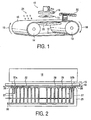
- a linear polisher 10 for use in practicing the present invention is shown.
- the linear polisher (also referred to as a linear planarization tool) 10 is utilized in planarizing a semiconductor wafer 11, such as a silicon wafer.
- CMP can be utilized to polish a base substrate
- typically CMP is utilized to remove a material layer (such as a film layer) or a portion of the material layer deposited on the semiconductor wafer.
- the material being removed can be the substrate material of the wafer itself or one of the layers formed on the substrate.
- Formed layers include dielectric materials (such as silicon dioxide), metals (such as aluminum, copper or tungsten) and alloys, or semiconductor materials (such as silicon or polysilicon).
- CMP is employed to planarize one or more of these layers fabricated on the wafer or is employed to expose an underlying topography while planarizing the surface.
- CMP involves patterned features formed on the surface of a wafer. For example, a dielectric layer (such as silicon dioxide) may be deposited over the surface, covering both raised features, as well as the underlying dielectric layer. Then, CMP is used to planarize the overlying silicon dioxide, so that the surface is substantially planarized. It is desirable to stop the polishing process at a point the raised features are exposed.
- a dielectric layer such as silicon dioxide
- dual damascene structures are fabricated by the use of CMP.
- CMP inter-level dielectric
- via and contact trench openings are patterned and formed in an inter-level dielectric (ILD) layer residing on a semiconductor wafer.
- a metal such as copper or aluminum
- a barrier layer such as TiN, Ta, TaN, etc
- CMP is used to polish away the excess metal material residing over the ILD, so that the metal resides only in the via and trench openings.
- CMP allows for the surface of the contact region (upper portion of the dual opening) to have a substantially planar surface, while the metal above the surface of the ILD is removed.
- CMP is utilized extensively to planarize film layers or formed features in which the planarization process is terminated at a particular point.
- the CMP is terminated when the metal is removed to expose the ILD.
- CMP ensures that the resultant structure has metal remaining only in the openings and that the upper surface of the ILD and the trench fill have a substantially planar surface.
- the art of performing CMP to polish away all or a portion of a layer formed on a wafer is known in the art.
- the linear polisher 10 of Figure 1 employs a linear planarization technology described above.
- the linear polisher 10 utilizes a belt 12, which moves linearly with respect to the surface of the wafer 11.
- the belt 12 is a continuous belt rotating about rollers (or spindles) 13 and 14, in which one roller or both is/are driven by a driving means, such as a motor, so that the rotational motion of the rollers 13, 14 causes the belt 12 to be driven in a linear motion (as shown by arrow 16) with respect to the wafer 11.
- the belt 12 is typically made from a metallic material.
- a polishing pad 15 is affixed onto the belt 12 at its outer surface facing the wafer 11.
- the pad can be made from a variety of materials, but is generally fibrous to provide an abrasive property.
- the belt can also be made from materials other than metal. In some instances, the pad 15 and the belt 12 are integrated as a single unit when fabricated. However constructed, the belt/pad assembly is made to move in a linear direction to
- the wafer 11 typically resides within a wafer carrier 18, which is part of a polishing head.
- the wafer 11 is held in position by a mechanical retaining means, such as a retainer ring, and/or by the use of vacuum.
- a mechanical retaining means such as a retainer ring
- a downforce is exerted to press the polishing head and carrier 18 downward, in order to engage the wafer onto the pad with some predetermined force.
- the linear polisher 10 also dispenses a slurry 21 onto the pad 15.
- a variety of dispensing devices and techniques are known in the art for dispensing the slurry 21.
- a pad conditioner 20 is typically used in order to recondition the pad surface during use. Techniques for reconditioning the pad 15 are also known in the art and generally require a constant scratching of the pad in order to remove the residue build-up caused by the used slurry and removed waste material.
- a support, platen or bearing 25 is disposed on the underside of belt 12 and opposite from the wafer 11, such that the belt/pad assembly resides between the bearing 25 and wafer 11.
- a primary purpose of bearing 25 is to provide a supporting platform on the underside of the belt 12 to ensure that the pad 15 makes sufficient contact with wafer 11 for uniform polishing. Since the belt 12 will depress when the wafer is pressed downward onto the pad 15, bearing 25 provides a necessary counteracting support to this downward force.
- the bearing 25 can be a solid platform or it can be a fluid bearing (also referred to as a fluid platen or support).
- a fluid bearing also referred to as a fluid platen or support.
- the fluid is generally air or liquid, although a neutral gas (such as nitrogen) can be used.
- a neutral gas such as nitrogen
- pressure variations exerted by the pad on the wafer can be adjusted to provide a more uniform polishing profile across the face of the wafer 11.
- a fluid bearing is disclosed in US Patent 5,558,568. Another example is described in a patent application titled "Control Of Chemical-Mechanical Polishing Rate Across A Substrate Surface For A Linear Polisher;" Serial No. 08/882,658; filed June 25, 1997.
- the fluid bearing 25 is positioned directly under the wafer 11, but on the opposite side of the belt 12.
- the wafer carrier 18 exerts a downforce to engage the wafer 11 on the pad 15, while the fluid flow from the fluid bearing exerts a counter-acting force to the underside of the belt 12.
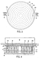
- a plurality of channels 27 are distributed within the body of the bearing 25 with openings 28 disposed along the upper surface. In some instances, the channels 27 open into corresponding concentric grooves 29 formed along the upper surface region of the fluid bearing 25, so that fluid flow from a given opening 28 feeds fluid into the corresponding groove or grooves 29.
- a cover plate (or insert) 32 is then placed atop the bearing 25 to fit over the grooves 29.
- a plurality of openings 34 are distributed on the cover plate 32, so that each ring 33 coincides with a corresponding groove 29.
- the openings 34 of each concentrically arranged ring 33 are fed by fluid flow from the corresponding groove 29.
- a single inlet 30 is shown for feeding each of the channels 27.
- the channels 27 could be coupled separately or in groups to separate inlets for individual (or group) flow control.
- Figures 2 and 3 show just one arrangement of openings on the surface of the bearing 25 to discharge the fluid and that the concentrically arranged openings 34 are but one example of how the openings can be configured.
- the fluid pressure at the openings 28 can be regulated or adjusted, as well. That is, by adjusting the fluid flow at the inlet 30, fluid pressure at the openings 34 can be adjusted.
- the above-mentioned patent application titled "Control Of Chemical-Mechanical Polishing Rate Across A Substrate Surface For A Linear Polisher" describes a fluid bearing having adjustable fluid pressure at the openings.
- each channel, a grouping of channels or portions of one or more rings can be configured for independent fluid pressure control.
- fluid pressure at different locations along the bearing surface can be controlled or adjusted separately.
- a variety of fluid bearings can be implemented for the fluid bearing 25. The number of such fluid channels, openings and arrangement are design choices.
- the present invention uses sensors 37 to determine the end-point of a polishing process.
- the sensors are disposed within the fluid bearing 25. It is appreciated that a number of sensors 37 can be located at various sensing points along the surface of the fluid bearing or they can be located elsewhere (even away from the bearing itself), in which instance such sensors are coupled to sensing input locations along the surface of the fluid bearing by the use of electrical, hydraulic or pneumatic lines, etc.
- two sensors 37 are shown disposed along the surface of the fluid bearing 25.
- the exact number and placement of such sensors is a design choice, but may be dependent on the type of parameters being measured or information being sought.
- the sensors employed can measure a variety of parameters which can provide information relating to the on-going polishing process.
- U.S. Patent 5,762,536 describes the use of sensors for monitoring various polishing parameters. The example illustrated in the '536 patent shows five sensors dispersed along the face of the platen.
- One type of sensor employed is a pressure sensor to measure the pressure exerted by the fluid flowing between the fluid bearing 25 and the underside of the belt 12.
- a leading edge sensor is labeled 37a and a trailing edge sensor is labeled 37b.
- the leading edge is defined as the edge of the wafer 11 first making contact with a point located on the linearly moving pad 15.
- the trailing edge is defined as the edge of the wafer 11 where the pad 15 disengages from the wafer.
- the leading edge sensor 37a is disposed near the edge where a point on the belt 12 first engages the fluid bearing 25, while the trailing edge sensor 37b is located at the opposite edge of the bearing 25 along the linear direction traveled by the belt 12.
- pressure sensors are utilized for sensors 37a-b.
- the fluid flow onto the fluid bearing 25 disperses fluid along the surface of the fluid bearing 25. Since the belt 12 is within close proximity of the bearing surface, the area between the fluid bearing 25 and the underside of the belt 12 is also filled with the fluid. Adequate fluid flow ensures that this space is filled with fluid, so that pressure sensors 37 will measure the pressure of the dispersed fluid.
- U.S. Patent 5,762,536 describes the use of pressure sensors to measure fluid pressure.
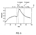
- Figure 4 illustrates one instance where there is a change in the fluid pressure.
- the wafer 11 is shown tilted slightly so as to depress the leading edge of the pad downward towards the sensor. Assuming the other parameters had been kept constant, this slight tilt causes the fluid pressure under the leading edge region to increase.
- the pressure increase is noted by the leading edge sensor 37a. That is, changes in the pressure at the leading edge can be detected by the leading edge sensor 37a.
- the motion of the wafer 11 may cause an increase of fluid pressure at the leading edge and a slight decrease at the trailing edge, or vice versa. Accordingly, depending on the process, some process variations can be detected by a change in the pressure at the leading edge, the trailing edge, or the pressure differential between the leading edge and trailing edge locations.
- This monitoring of the increase (or decrease) in the fluid pressure can be utilized to identify certain process parameters.
- the present invention looks at the fluid pressure changes to detect an end point condition. It has been determined through experimentation that the pad/wafer sliding interface results in a shear force that is counteracted by a gradient in the fluid bearing pressure within the bearing-belt gap. This resulting pressure gradient is generally in the direction of belt travel, so that an increase in the shear force will increase the pressure at the leading edge region, somewhat similar to the result obtained in the illustrated example of Figure 4.
- the shear force will depend on the material being polished. Accordingly, a change in the material being polished will change the magnitude of the shear force, which causes a change in the pressure at the leading edge of the fluid bearing.
- This pressure change when appropriately monitored, can identify an end point condition. That is, when one material is polished away to reveal an underlying material of different composition (the end point of the polishing process), the shear force changes accordingly.
- the change in the shear force causes a change in the fluid pressure, most notably at the leading edge.
- This fluid pressure change is detected by the leading edge pressure sensor 37a. Therefore, a polishing end point can be detected by noticing a change in the fluid pressure residing above the fluid bearing 25.
- a material stack comprised of copper/tantalum/silicon dioxide on a silicon wafer (Cu/Ta/SiO 2 /Si) was polished using CMP on a linear planarization tool. Normalized fluid pressure values at the leading edge sensor 37a is graphed versus polishing time (arbitrary time scale is noted in the Figure).
- the Cu/Ta/SiO 2 /Si stack is equivalent to the polishing of copper (which is separated from the SiO 2 by a thin barrier layer of tantalum).
- the fluid pressure increases slightly as the Cu is polished away. Then, as the underlying Ta begins to be exposed so that both Cu and Ta are being polished, a rapid increase in the fluid pressure is noted. A peak pressure is reached where only Ta is being polished. Subsequently, as Ta is polished away exposing the underlying SiO 2 , the fluid pressure begins to decline and continues to do so until all of the Ta is removed.
- a desired polishing end point can be detected by monitoring the fluid pressure.
- the first abrupt change noted in the graph 40 occurs when Ta begins to be polished, culminating near a peak value when Cu has been polished away.
- Cu polishing end point can be determined at or near the peak fluid pressure value (as noted in the drawing).
- Ta polishing end point can be detected when the fluid pressure drops from the peak and reaches a preset value (also noted in the drawing). At this point, Cu and Ta will have been removed from above the ILD, so that the exposed Cu would reside in the openings formed in the ILD.
- FIG. 6A a portion of a semiconductor device 42 having a dual damascene structure 43 is shown.
- the dual damascene structure 43 is comprised of a via opening 44 and a contact trench opening 45 and is formed in a dielectric layer 46, which is typically referred to as an ILD.
- the via 44 is utilized to connect to an underlying conductive region. In the example, via 44 connects to an underlying metal layer 41.
- a barrier layer 47 is deposited.
- One of the barrier materials previously described (such as TiN, Ta, TaN) is deposited as a barrier liner when copper metallization is utilized, since copper will readily diffuse into the ILD. Typically, the barrier layer is conformally deposited.
- copper 48 is deposited over the wafer to fill in the via and trench openings 44, 45. When aluminum metallization is used, a barrier layer to isolate the metal from the ILD is typically not necessary.
- CMP is utilized to planarize the surface of the structure, so that the copper 48 remaining is only within the via and trench regions.
- the dual damascene structure is copper-filled.
- the CMP planarization is achieved by the practice of the linear planarization technique and the end point for the CMP is achieved by the practice of the present invention as previously described.
- the copper and the barrier material are polished away, thereby exposing the underlying upper surface of the ILD, the fluid pressure changes being monitored will indicate when this end point has been reached.
- the CMP process is stopped.
- the dotted line 49 indicates what could result if the end point is not detected and the polishing is permitted to continue.
- the additional polishing can polish away portions of the metal residing within the trench region 45.
- equivalent material response graphs can be experimentally obtained for the various materials being polished to detect the polishing end point.
- the response will also depend on the underlying material being exposed.
- the response curve can be utilized in a manufacturing setting to monitor an on-going process to detect an end point of a CMP polishing step. Accordingly, in-situ end point detection can be practiced in which the end point detection sensor is located below the polishing pad.
- two pressure sensors 37a, 37b are utilized.
- the pressure being monitored is from the leading edge sensor 37a.
- the present invention can be practiced utilizing only one sensor 37, which is located at the leading edge for optimum response. It is appreciated that the sensor 37a could be located elsewhere as well to provide the end point detection. However, the preference is to have it at the leading edge.
- the second sensor 37b is utilized for providing a fluid pressure response at the trailing edge, but is not necessarily needed for the practice of the present invention.
- the second sensor 37b is utilized in the for providing a fluid pressure response at the trailing edge for comparison purpose with the leading edge sensor.
- pressure differential between the two sensor locations can be monitored for polishing uniformity of a given layer.
- the pressure differential of the two sensors could also be used for end point detection, instead of just the leading edge sensor. The use of particular sensor or sensors and the location of such sensor(s) will depend on the polishing process being monitored.
- the present scheme monitors the fluid pressure between the fluid bearing and the underside of the belt to obtain end point detection of a CMP process.
- the sensors described are pressure sensors, but other types of sensors can be readily adapted for measuring the change in the shear force or effects caused by such changes.
- the fluid bearing can be operated either with air gas or liquid, but the preference is to use air or de-ionized (D.I.) water.
- the above example illustrates a condition where the change in the shear force is appreciable, so that a noticeable pressure change is detected at the process end point.
- a transition between dissimilar metals having different hardness or between a metal and a dielectric will result in a noticeable change in the shear force, which then can be detected by the pressure sensor.
- the transition from one to the other may not result in an appreciable change in the shear force. For example, polishing of one dielectric to expose another may be difficult to detect due to the closeness of the forces associated with the materials involved.
- the present invention looks to the zeta potential of the materials involved and selects a particular slurry which can enhance the detection of the polishing end point, by introducing a zeta potential of an opposite polarity. That is, the present invention utilizes or exploits the difference in the zeta potential between materials to determine the polishing end point.
- the zeta potential difference enhances the frictional shear force differential, so that the above described fluid pressure sensing technique can still be used to provide the end point detection.
- abrasive particles in colloidal suspension in the slurry acquire an electric charge and remain in suspension because of mutual electrostatic repulsive force. There exists a charge distribution between the charged colloidal particle and the bulk of the solution in the slurry. The presence of this charge results in a potential difference between the surface of the abrasive particle and the solution.
- the potential at the surface of the abrasive particle (also referred to as colloid) is referred to as the surface potential.
- zeta potential occurs at the junction or boundary of the moving particle and the liquid.
- This boundary also referred to as the slip plane
- the Stem layer is considered to be rigidly attached to the colloid, while the diffuse layer is not (see "Zeta Potential: A complete course in 5 Minutes;" Zeta-Meter Inc. brochure at pp. 1-8).
- the electrical potential at this junction is related to the mobility of the particle, and believed to be more significant than the surface potential.
- the zeta potential of the particle can be easily measured under the influence of an electric field. For example, a Coulter Delsa 440 SX Zeta Potential and Particle Size measuring tool (by Coulter International Corp.) measures the electrophoretic mobility by laser Doppler velocimetry to determine the zeta potential.
- the zeta potential is also related to the repulsion and attraction forces of two particles.
- stability of particles in suspension is determined by a balance of two opposing forces.
- One is the electrostatic repulsive force, while the other is the van der Waals attractive force (see, the Zeta-meter Inc. reference noted above).
- Particles overcoming the electrostatic repulsion barrier typically will agglomerate.
- monitoring the zeta potential can identify the behavior of the particles In the solution.
- the behavior of the particle in the solution can also be controlled.
- fluid viscosity, flocculation and coagulation are some properties which can be controlled by adjusting the zeta potential of a fluid.
- graph 50 illustrates the zeta potentials of three compounds as the pH level changes.
- the graph 50 shows the zeta potential versus pH for SiO 2 , Si 3 N 4 and Al 2 O 3 .
- the zeta potential for each of the compounds is dependent on the pH level of the medium.
- the zeta potential changes polarity at a given pH level. Accordingly, the pH level of the medium can be selected so that the zeta potential of the particles present in the slurry will be at a particular value and polarity.
- the present invention exploits this zeta potential variation to detect an end point of a CMP processing step. From the above description, it is appreciated that the abrasive particles present in the slurry possess a zeta potential, which affects how the particles respond to the polishing (or planarizing) process. Likewise, the film surface (of the material being polished) immersed in the slurry also acquires surface and zeta potentials as the material is polished. The zeta potential of the film will be separate from the zeta potential of the abrasive particles.
- the abrasive particles of the slurry can be selected to have a zeta potential of one polarity, while the film material being polished can be selected to have a zeta potential of the opposite polarity.
- the zero zeta potential (or zeta potential polarity cross-over) point is approximately at a pH of 2.7 for SiO 2 and 4.5 for Si 3 N 4 .
- a slurry having a pH level in the range of 3 to 4 wiii cause the SiO 2 material to have a negative zeta potential, while Si 3 N 4 material will have a positive zeta potential. If the slurry selected has SiO 2 abrasive particles suspended in the solution, at a pH of 3 to 4, the SiO 2 particles will have a negative zeta potential value.
- both the SiO 2 slurry particles and the SiO 2 film will have a negative zeta potential. There is no appreciable difference in the zeta potentials of the abrasive particles and the film layer being polished.
- the zeta potential of Si 3 N 4 would be positive at the pH range of 3 to 4.
- the zeta potential polarity of the Si 3 N 4 film is opposite from that of the SiO 2 abrasive particles of the slurry. The polarity difference in the zeta potentials of the abrasive particles and the film layer being polished is exploited to detect the end point of a polishing process.
- the layer being polished away is SiO 2 and the underlying layer is Si 3 N 4 . Since the SiO 2 is being polished away to expose the underlying Si 3 N 4 , it would be beneficial to stop the polishing process when the Si 3 N 4 is exposed. While the SiO 2 is being polished, the zeta potential will have a negative value for the material being polished. When the Si 3 N 4 is exposed, the Si 3 N 4 film will exhibit a zeta potential of the opposite polarity. This noticeable change in the zeta potential is exploited to provide a detection mechanism for determining the endpoint for polishing away the SiO2 layer.
- the above example illustrates the practice of the invention in which the zeta potential can be exploited to determine the end point of a CMP process.
- the zeta potentials can be selected so that when one layer (or portion of a layer) is polished away to expose an underlying layer, a noticeable change occurs in the zeta potentials of the materials involved. A monitoring scheme can then detect this change in the zeta potentials.
- a variety of techniques can be used to ensure that the two materials will have differing zeta potentials when being polished. Specialized slurry chemistries can be selected, additives can be introduced into the slurry, or other means which ensure a differing zeta potential between the two materials being polished can be employed.
- the preferred technique controls the pH operating level of the slurry to ensure a point of operation which causes the two materials (the material being polished and the underlying material) to have noticeable zeta potential differences.
- the preferred technique is to ensure that the two materials have opposite zeta potential polarities at the operating pH of the slurry. Thus, when the overlying layer is polished away to expose the underlying layer (at which point the polishing should terminate), a polarity change in the zeta potential occurs. This polarity difference is exploited to detect the end point for the polishing.
- both will have negative zeta potentials at a slurry pH level in the range of 3 to 4.
- the particles in the slurry and the film will be in electrostatic repulsion, due to the negative zeta potentials.
- the positive zeta potential of the Si 3 N 4 film will introduce an attractive force to the abrasive particles of the slurry. This attraction force will then induce an increase in the frictional force, since the particles tend to combine (amalgamate). This increase in the frictional force is manifested as an increase in the shear force at the wafer-pad interface and detected as an increase in the fluid pressure at the leading edge sensor 37a.
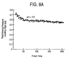
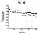
- FIGS 8A and 8B Experimental results of detecting a CMP end point in polishing a film stack of PTEOS/Si 3 N 4 /SiO 2 disposed on a Si wafer are shown in Figures 8A and 8B, in which the leading edge sensor of a fluid bearing is used to detect the fluid pressure change.
- PTEOS plasma enhanced tetra ethyl ortho silicate glass
- a silica-based slurry having a pH level of approximately 7.0 is selected for performing the CMP.
- the appreciable zeta potential change causes a change at the wafer-pad interface.
- a change in the zeta potential polarity causes the Si 3 N 4 film to be attracted to the abrasive particles of the slurry, which induces an increase in the shear force at the wafer-pad interface.
- This increase in the shear force is detected at or near the leading edge by the sensor 37a, as an increase in the fluid pressure residing between the belt and the fluid bearing.
- the senor 37a could be located elsewhere as well to provide the end point detection. However, the preference is to have it at the leading edge.
- the second sensor 37b is utilized in the present instance for providing a fluid pressure response at the trailing edge for comparison purpose with the leading edge sensor. For example, pressure differential between the two sensor locations can be monitored for polishing uniformity of a given layer. The pressure differential of the two sensors could also be used for end point detection, instead of just the leading edge sensor.
- the technique of utilizing leading edge pressure variations is sometimes difficult or impossible to achieve without some form of additional aid.
- the zeta potential is exploited to differentiate a response characteristic when one material is polished away exposing an underlying material.
- the present invention detects the effects of the zeta potential variation by measuring the fluid pressure disposed between the fluid bearing and the belt/pad assembly.
- a particular slurry pH level is selected to cause the zeta potential of the two materials to have opposite polarity at that pH level, so that the difference in the polarity causes a noticeable change in the frictional force, which is detected by the fluid bearing pressure sensor.
- the sensor utilized is the leading edge sensor of the linear polisher.
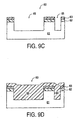
- FIGs 9A-F An application of the above described CMP process to planarize a SiO 2 layer, in which Si 3 N 4 is used for the polishing end point is illustrated in Figures 9A-F.
- a structure 60 is shown, having a silicon substrate 61 upon which a SiO 2 layer 62 is formed. Atop the SiO 2 layer 62, a Si 3 N 4 layer 63 is formed (see Figure 9A).
- a photoresistive layer 64 is deposited and patterned to expose portions of the substrate 61 (see Figure 9B). Then, using a known etching step, the exposed substrate is etched to form openings 65 (see Figure 9C).
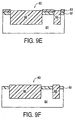
- a second SiO 2 layer 66 is blanket deposited over the structure, also filling in the openings 65 (see Figure 9D). Then, CMP is performed to planarize the SiO 2 layer 66. The end point detection scheme described above is employed to determine when the underlying portions of the Si 3 N 4 layer 63 is exposed.
- the resulting structure has the SiO 2 in the openings 65, but not over the upper surface of the Si 3 N 4 (see Figure 9E).
- the upper surface of the SiO 2 in the openings 65 is slightly below the level of the Si 3 N 4 layer 63.
- the exposed Si 3 N 4 layer 63 is etched away by a known technique, so that the upper surface of the structure is covered by SiO 2 (see Figure 9F).
- the portion of the SiO 2 material 66 residing at the openings 65 is slightly higher as compared to the SiO 2 material 62 which had been residing below the Si 3 N 4 layer 63.
- the structure formed is part of a shallow trench isolation structure. As noted above, the structure is formed by the application of CMP and in which the present invention can be practiced to detect the end point of the CMP step.
- the present invention is described in reference to performing CMP on a semiconductor wafer, the invention can be readily adapted to polish other materials as well, such as glass, metal substrates or other semiconductor substrates, including substrates for use in manufacturing flat panel displays.
Landscapes
- Engineering & Computer Science (AREA)
- Mechanical Engineering (AREA)
- Physics & Mathematics (AREA)
- Condensed Matter Physics & Semiconductors (AREA)
- General Physics & Mathematics (AREA)
- Manufacturing & Machinery (AREA)
- Computer Hardware Design (AREA)
- Microelectronics & Electronic Packaging (AREA)
- Power Engineering (AREA)
- Mechanical Treatment Of Semiconductor (AREA)
- Finish Polishing, Edge Sharpening, And Grinding By Specific Grinding Devices (AREA)
- Weting (AREA)
Applications Claiming Priority (3)
| Application Number | Priority Date | Filing Date | Title |
|---|---|---|---|
| US182570 | 1998-10-29 | ||
| US09/182,570 US6325706B1 (en) | 1998-10-29 | 1998-10-29 | Use of zeta potential during chemical mechanical polishing for end point detection |
| PCT/US1999/023662 WO2000025983A1 (en) | 1998-10-29 | 1999-10-13 | Use of zeta potential during chemical mechanical polishing for end point detection |
Publications (2)
| Publication Number | Publication Date |
|---|---|
| EP1124666A1 EP1124666A1 (en) | 2001-08-22 |
| EP1124666B1 true EP1124666B1 (en) | 2002-08-14 |
Family
ID=22669046
Family Applications (1)
| Application Number | Title | Priority Date | Filing Date |
|---|---|---|---|
| EP99950284A Expired - Lifetime EP1124666B1 (en) | 1998-10-29 | 1999-10-13 | Use of zeta potential during chemical mechanical polishing for end point detection |
Country Status (9)
| Country | Link |
|---|---|
| US (1) | US6325706B1 (enExample) |
| EP (1) | EP1124666B1 (enExample) |
| JP (1) | JP2002528928A (enExample) |
| KR (1) | KR100637568B1 (enExample) |
| AT (1) | ATE222158T1 (enExample) |
| AU (1) | AU6297799A (enExample) |
| DE (1) | DE69902553T2 (enExample) |
| TW (1) | TW445535B (enExample) |
| WO (1) | WO2000025983A1 (enExample) |
Families Citing this family (38)
| Publication number | Priority date | Publication date | Assignee | Title |
|---|---|---|---|---|
| JP3702668B2 (ja) * | 1998-09-28 | 2005-10-05 | 株式会社村田製作所 | 電子部品チップ供給装置 |
| US6492273B1 (en) * | 1999-08-31 | 2002-12-10 | Micron Technology, Inc. | Methods and apparatuses for monitoring and controlling mechanical or chemical-mechanical planarization of microelectronic substrate assemblies |
| US6520833B1 (en) * | 2000-06-30 | 2003-02-18 | Lam Research Corporation | Oscillating fixed abrasive CMP system and methods for implementing the same |
| US6375540B1 (en) * | 2000-06-30 | 2002-04-23 | Lam Research Corporation | End-point detection system for chemical mechanical posing applications |
| US6520834B1 (en) * | 2000-08-09 | 2003-02-18 | Micron Technology, Inc. | Methods and apparatuses for analyzing and controlling performance parameters in mechanical and chemical-mechanical planarization of microelectronic substrates |
| US6439978B1 (en) * | 2000-09-07 | 2002-08-27 | Oliver Design, Inc. | Substrate polishing system using roll-to-roll fixed abrasive |
| US6607425B1 (en) * | 2000-12-21 | 2003-08-19 | Lam Research Corporation | Pressurized membrane platen design for improving performance in CMP applications |
| JP5027377B2 (ja) * | 2001-06-26 | 2012-09-19 | アプライド マテリアルズ インコーポレイテッド | 化学的機械研磨のためのエンドポイント検出システム |
| US6656024B1 (en) * | 2001-12-21 | 2003-12-02 | Lam Research Corporation | Method and apparatus for reducing compressed dry air usage during chemical mechanical planarization |
| US6653202B1 (en) * | 2003-01-17 | 2003-11-25 | Advanced Micro Devices, Inc. | Method of shallow trench isolation (STI) formation using amorphous carbon |
| DE10325406B4 (de) * | 2003-06-05 | 2005-04-28 | Eads Deutschland Gmbh | Schadensermittlung an zu prüfenden Strukturen mittels Ultraschall |
| US20050118932A1 (en) * | 2003-07-03 | 2005-06-02 | Homayoun Talieh | Adjustable gap chemical mechanical polishing method and apparatus |
| US6955588B1 (en) * | 2004-03-31 | 2005-10-18 | Lam Research Corporation | Method of and platen for controlling removal rate characteristics in chemical mechanical planarization |
| US7120553B2 (en) * | 2004-07-22 | 2006-10-10 | Applied Materials, Inc. | Iso-reflectance wavelengths |
| US7153182B1 (en) * | 2004-09-30 | 2006-12-26 | Lam Research Corporation | System and method for in situ characterization and maintenance of polishing pad smoothness in chemical mechanical polishing |
| DE102004054920B4 (de) * | 2004-11-09 | 2008-01-31 | Fraunhofer-Gesellschaft zur Förderung der angewandten Forschung e.V. | Bauteil und Vorrichtung zur Steuerung von physikalischen Parametern mit mindestens einem Bauteil |
| DE102006018276A1 (de) * | 2006-04-20 | 2007-10-31 | Conti Temic Microelectronic Gmbh | Verfahren und Vorrichtung zur Schliffpräparation eines mehrere ebene und zueinander parallel verlaufende Schichten unterschiedlichen Materials aufweisenden Probenkörpers |
| US8626458B2 (en) * | 2009-11-05 | 2014-01-07 | Vibration Technologies, Llc | Method and system for measuring the dynamic response of a structure during a machining process |
| JP5819076B2 (ja) * | 2010-03-10 | 2015-11-18 | 株式会社フジミインコーポレーテッド | 研磨用組成物 |
| US20130017762A1 (en) * | 2011-07-15 | 2013-01-17 | Infineon Technologies Ag | Method and Apparatus for Determining a Measure of a Thickness of a Polishing Pad of a Polishing Machine |
| US9259821B2 (en) | 2014-06-25 | 2016-02-16 | Rohm And Haas Electronic Materials Cmp Holdings, Inc. | Chemical mechanical polishing layer formulation with conditioning tolerance |
| US9873180B2 (en) | 2014-10-17 | 2018-01-23 | Applied Materials, Inc. | CMP pad construction with composite material properties using additive manufacturing processes |
| US11745302B2 (en) | 2014-10-17 | 2023-09-05 | Applied Materials, Inc. | Methods and precursor formulations for forming advanced polishing pads by use of an additive manufacturing process |
| CN107078048B (zh) | 2014-10-17 | 2021-08-13 | 应用材料公司 | 使用加成制造工艺的具复合材料特性的cmp衬垫建构 |
| US10875153B2 (en) | 2014-10-17 | 2020-12-29 | Applied Materials, Inc. | Advanced polishing pad materials and formulations |
| US9776361B2 (en) | 2014-10-17 | 2017-10-03 | Applied Materials, Inc. | Polishing articles and integrated system and methods for manufacturing chemical mechanical polishing articles |
| KR20230169424A (ko) | 2015-10-30 | 2023-12-15 | 어플라이드 머티어리얼스, 인코포레이티드 | 원하는 제타 전위를 가진 연마 제품을 형성하는 장치 및 방법 |
| US10593574B2 (en) | 2015-11-06 | 2020-03-17 | Applied Materials, Inc. | Techniques for combining CMP process tracking data with 3D printed CMP consumables |
| US10391605B2 (en) | 2016-01-19 | 2019-08-27 | Applied Materials, Inc. | Method and apparatus for forming porous advanced polishing pads using an additive manufacturing process |
| DE102016214568A1 (de) * | 2016-08-05 | 2018-02-08 | Weeke Bohrsysteme Gmbh | Bearbeitungsvorrichtung und Bearbeitungsverfahren |
| US11130686B2 (en) | 2017-01-10 | 2021-09-28 | Vermeer Manufacturing Company | Systems and methods for dosing slurries to remove suspended solids |
| US11471999B2 (en) | 2017-07-26 | 2022-10-18 | Applied Materials, Inc. | Integrated abrasive polishing pads and manufacturing methods |
| WO2019022961A1 (en) * | 2017-07-28 | 2019-01-31 | Applied Materials, Inc. | METHOD FOR IDENTIFYING AND MONITORING ROLLER ROLL POLISHING PAD MATERIALS DURING PROCESSING |
| WO2019032286A1 (en) | 2017-08-07 | 2019-02-14 | Applied Materials, Inc. | ABRASIVE DISTRIBUTION POLISHING PADS AND METHODS OF MAKING SAME |
| CN112654655A (zh) | 2018-09-04 | 2021-04-13 | 应用材料公司 | 先进抛光垫配方 |
| US11851570B2 (en) | 2019-04-12 | 2023-12-26 | Applied Materials, Inc. | Anionic polishing pads formed by printing processes |
| KR20220083915A (ko) * | 2020-12-11 | 2022-06-21 | 삼성디스플레이 주식회사 | 감지 센서를 포함하는 표시 장치 및 감지 센서 제조 방법 |
| US11878389B2 (en) | 2021-02-10 | 2024-01-23 | Applied Materials, Inc. | Structures formed using an additive manufacturing process for regenerating surface texture in situ |
Family Cites Families (20)
| Publication number | Priority date | Publication date | Assignee | Title |
|---|---|---|---|---|
| US4648715A (en) | 1982-09-07 | 1987-03-10 | Langley-Ford Instruments A Division Of Coulter Electronics Of N.E. | Electrophoretic light scattering with plural reference beams, apparatus and method |
| US4793895A (en) | 1988-01-25 | 1988-12-27 | Ibm Corporation | In situ conductivity monitoring technique for chemical/mechanical planarization endpoint detection |
| US5078801A (en) * | 1990-08-14 | 1992-01-07 | Intel Corporation | Post-polish cleaning of oxidized substrates by reverse colloidation |
| US5409544A (en) | 1990-08-20 | 1995-04-25 | Hitachi, Ltd. | Method of controlling adhesion of fine particles to an object in liquid |
| US5240552A (en) | 1991-12-11 | 1993-08-31 | Micron Technology, Inc. | Chemical mechanical planarization (CMP) of a semiconductor wafer using acoustical waves for in-situ end point detection |
| US5308438A (en) | 1992-01-30 | 1994-05-03 | International Business Machines Corporation | Endpoint detection apparatus and method for chemical/mechanical polishing |
| US5329732A (en) | 1992-06-15 | 1994-07-19 | Speedfam Corporation | Wafer polishing method and apparatus |
| US5265378A (en) * | 1992-07-10 | 1993-11-30 | Lsi Logic Corporation | Detecting the endpoint of chem-mech polishing and resulting semiconductor device |
| US5272117A (en) * | 1992-12-07 | 1993-12-21 | Motorola, Inc. | Method for planarizing a layer of material |
| US5433651A (en) | 1993-12-22 | 1995-07-18 | International Business Machines Corporation | In-situ endpoint detection and process monitoring method and apparatus for chemical-mechanical polishing |
| DE69512971T2 (de) | 1994-08-09 | 2000-05-18 | Ontrak Systems Inc., Milpitas | Linear Poliergerät und Wafer Planarisierungsverfahren |
| US5527423A (en) * | 1994-10-06 | 1996-06-18 | Cabot Corporation | Chemical mechanical polishing slurry for metal layers |
| US5593344A (en) * | 1994-10-11 | 1997-01-14 | Ontrak Systems, Inc. | Wafer polishing machine with fluid bearings and drive systems |
| US5668063A (en) | 1995-05-23 | 1997-09-16 | Watkins Johnson Company | Method of planarizing a layer of material |
| US5762536A (en) * | 1996-04-26 | 1998-06-09 | Lam Research Corporation | Sensors for a linear polisher |
| US5800248A (en) * | 1996-04-26 | 1998-09-01 | Ontrak Systems Inc. | Control of chemical-mechanical polishing rate across a substrate surface |
| KR100218309B1 (ko) | 1996-07-09 | 1999-09-01 | 구본준 | 씨엠피장치의 반도체웨이퍼 레벨링 감지장치 및 방법 |
| US5722877A (en) | 1996-10-11 | 1998-03-03 | Lam Research Corporation | Technique for improving within-wafer non-uniformity of material removal for performing CMP |
| US5980368A (en) | 1997-11-05 | 1999-11-09 | Aplex Group | Polishing tool having a sealed fluid chamber for support of polishing pad |
| US6186865B1 (en) * | 1998-10-29 | 2001-02-13 | Lam Research Corporation | Apparatus and method for performing end point detection on a linear planarization tool |
-
1998
- 1998-10-29 US US09/182,570 patent/US6325706B1/en not_active Expired - Fee Related
-
1999
- 1999-10-13 EP EP99950284A patent/EP1124666B1/en not_active Expired - Lifetime
- 1999-10-13 AT AT99950284T patent/ATE222158T1/de not_active IP Right Cessation
- 1999-10-13 WO PCT/US1999/023662 patent/WO2000025983A1/en not_active Ceased
- 1999-10-13 AU AU62977/99A patent/AU6297799A/en not_active Abandoned
- 1999-10-13 KR KR1020017005154A patent/KR100637568B1/ko not_active Expired - Fee Related
- 1999-10-13 JP JP2000579404A patent/JP2002528928A/ja active Pending
- 1999-10-13 DE DE69902553T patent/DE69902553T2/de not_active Expired - Fee Related
-
2000
- 2000-01-15 TW TW088118704A patent/TW445535B/zh not_active IP Right Cessation
Also Published As
| Publication number | Publication date |
|---|---|
| ATE222158T1 (de) | 2002-08-15 |
| KR20010085953A (ko) | 2001-09-07 |
| US6325706B1 (en) | 2001-12-04 |
| JP2002528928A (ja) | 2002-09-03 |
| WO2000025983A1 (en) | 2000-05-11 |
| AU6297799A (en) | 2000-05-22 |
| KR100637568B1 (ko) | 2006-10-20 |
| DE69902553D1 (de) | 2002-09-19 |
| DE69902553T2 (de) | 2003-04-24 |
| TW445535B (en) | 2001-07-11 |
| EP1124666A1 (en) | 2001-08-22 |
Similar Documents
| Publication | Publication Date | Title |
|---|---|---|
| EP1124666B1 (en) | Use of zeta potential during chemical mechanical polishing for end point detection | |
| US6186865B1 (en) | Apparatus and method for performing end point detection on a linear planarization tool | |
| US5762536A (en) | Sensors for a linear polisher | |
| EP0771611B1 (en) | Method and apparatus for determining endpoint in polishing process | |
| US6007408A (en) | Method and apparatus for endpointing mechanical and chemical-mechanical polishing of substrates | |
| US6458013B1 (en) | Method of chemical mechanical polishing | |
| JP3811193B2 (ja) | 研磨装置及び研磨方法 | |
| USRE38029E1 (en) | Wafer polishing and endpoint detection | |
| US6645865B2 (en) | Methods, apparatuses and substrate assembly structures for fabricating microelectronic components using mechanical and chemical-mechanical planarization processes | |
| US6837774B2 (en) | Linear chemical mechanical polishing apparatus equipped with programmable pneumatic support platen and method of using | |
| TW542768B (en) | Device and method for polishing a semiconductor substrate | |
| JPH09290367A (ja) | 化学的−機械的研磨及び終点検出のために使用されるウエハ研磨機ヘッド | |
| JP2002530861A (ja) | 金属半導体構造体におけるcmp時のディッシング速度を低下させる方法 | |
| US6432823B1 (en) | Off-concentric polishing system design | |
| US6340434B1 (en) | Method and apparatus for chemical-mechanical polishing | |
| US6099387A (en) | CMP of a circlet wafer using disc-like brake polish pads | |
| US6686284B2 (en) | Chemical mechanical polisher equipped with chilled retaining ring and method of using | |
| US7153182B1 (en) | System and method for in situ characterization and maintenance of polishing pad smoothness in chemical mechanical polishing | |
| JP2008205464A (ja) | 半導体基板の研磨方法 | |
| KR20030029119A (ko) | 기판의 화학적 기계 폴리싱 장치 및 방법 | |
| US6268224B1 (en) | Method and apparatus for detecting an ion-implanted polishing endpoint layer within a semiconductor wafer | |
| Tsujimura | Chemical mechanical polishing (CMP) removal rate uniformity and role of carrier parameters | |
| US7828625B2 (en) | Method of supplying polishing liquid | |
| KR19980048965A (ko) | 텅스텐 화학 및 기계적 연마장치 및 연마방법 | |
| JPH0955361A (ja) | 半導体製造装置及び半導体製造装置の使用方法及び半導体装置の製造方法 |
Legal Events
| Date | Code | Title | Description |
|---|---|---|---|
| PUAI | Public reference made under article 153(3) epc to a published international application that has entered the european phase |
Free format text: ORIGINAL CODE: 0009012 |
|
| 17P | Request for examination filed |
Effective date: 20010424 |
|
| AK | Designated contracting states |
Kind code of ref document: A1 Designated state(s): AT BE CH CY DE DK ES FI FR GB GR IE IT LI LU MC NL PT SE |
|
| RIN1 | Information on inventor provided before grant (corrected) |
Inventor name: PANT, ANIL, K. Inventor name: NAGENGAST, ANDREW, J. Inventor name: KRUSELL, WILBUR, C. |
|
| RTI1 | Title (correction) |
Free format text: USE OF ZETA POTENTIAL DURING CHEMICAL MECHANICAL POLISHING FOR END POINT DETECTION |
|
| GRAG | Despatch of communication of intention to grant |
Free format text: ORIGINAL CODE: EPIDOS AGRA |
|
| 17Q | First examination report despatched |
Effective date: 20011220 |
|
| GRAG | Despatch of communication of intention to grant |
Free format text: ORIGINAL CODE: EPIDOS AGRA |
|
| GRAH | Despatch of communication of intention to grant a patent |
Free format text: ORIGINAL CODE: EPIDOS IGRA |
|
| GRAH | Despatch of communication of intention to grant a patent |
Free format text: ORIGINAL CODE: EPIDOS IGRA |
|
| GRAA | (expected) grant |
Free format text: ORIGINAL CODE: 0009210 |
|
| AK | Designated contracting states |
Kind code of ref document: B1 Designated state(s): AT DE FR GB IT |
|
| REF | Corresponds to: |
Ref document number: 222158 Country of ref document: AT Date of ref document: 20020815 Kind code of ref document: T |
|
| REG | Reference to a national code |
Ref country code: GB Ref legal event code: FG4D |
|
| REF | Corresponds to: |
Ref document number: 69902553 Country of ref document: DE Date of ref document: 20020919 |
|
| ET | Fr: translation filed | ||
| PLBE | No opposition filed within time limit |
Free format text: ORIGINAL CODE: 0009261 |
|
| STAA | Information on the status of an ep patent application or granted ep patent |
Free format text: STATUS: NO OPPOSITION FILED WITHIN TIME LIMIT |
|
| 26N | No opposition filed |
Effective date: 20030515 |
|
| PGFP | Annual fee paid to national office [announced via postgrant information from national office to epo] |
Ref country code: DE Payment date: 20071130 Year of fee payment: 9 |
|
| PGFP | Annual fee paid to national office [announced via postgrant information from national office to epo] |
Ref country code: AT Payment date: 20070919 Year of fee payment: 9 Ref country code: IT Payment date: 20071026 Year of fee payment: 9 |
|
| PGFP | Annual fee paid to national office [announced via postgrant information from national office to epo] |
Ref country code: GB Payment date: 20071029 Year of fee payment: 9 Ref country code: FR Payment date: 20071017 Year of fee payment: 9 |
|
| GBPC | Gb: european patent ceased through non-payment of renewal fee |
Effective date: 20081013 |
|
| REG | Reference to a national code |
Ref country code: FR Ref legal event code: ST Effective date: 20090630 |
|
| PG25 | Lapsed in a contracting state [announced via postgrant information from national office to epo] |
Ref country code: IT Free format text: LAPSE BECAUSE OF NON-PAYMENT OF DUE FEES Effective date: 20081013 Ref country code: DE Free format text: LAPSE BECAUSE OF NON-PAYMENT OF DUE FEES Effective date: 20090501 Ref country code: AT Free format text: LAPSE BECAUSE OF NON-PAYMENT OF DUE FEES Effective date: 20081013 |
|
| PG25 | Lapsed in a contracting state [announced via postgrant information from national office to epo] |
Ref country code: FR Free format text: LAPSE BECAUSE OF NON-PAYMENT OF DUE FEES Effective date: 20081031 |
|
| PG25 | Lapsed in a contracting state [announced via postgrant information from national office to epo] |
Ref country code: GB Free format text: LAPSE BECAUSE OF NON-PAYMENT OF DUE FEES Effective date: 20081013 |