EP1124247A1 - Metallenthaltende Zusammensetzung zum Erzeugen einer elektronenemittierenden Vorrichtung und Verfahren zur Herstellung einer elektronenemittierenden Vorrichtung, einer Elektronenquelle und eines Bilderzeugungsgerätes - Google Patents
Metallenthaltende Zusammensetzung zum Erzeugen einer elektronenemittierenden Vorrichtung und Verfahren zur Herstellung einer elektronenemittierenden Vorrichtung, einer Elektronenquelle und eines Bilderzeugungsgerätes Download PDFInfo
- Publication number
- EP1124247A1 EP1124247A1 EP01201600A EP01201600A EP1124247A1 EP 1124247 A1 EP1124247 A1 EP 1124247A1 EP 01201600 A EP01201600 A EP 01201600A EP 01201600 A EP01201600 A EP 01201600A EP 1124247 A1 EP1124247 A1 EP 1124247A1
- Authority
- EP
- European Patent Office
- Prior art keywords
- electron
- metal
- substrate
- emitting
- film
- Prior art date
- Legal status (The legal status is an assumption and is not a legal conclusion. Google has not performed a legal analysis and makes no representation as to the accuracy of the status listed.)
- Withdrawn
Links
Images


Classifications
-
- H—ELECTRICITY
- H01—ELECTRIC ELEMENTS
- H01J—ELECTRIC DISCHARGE TUBES OR DISCHARGE LAMPS
- H01J1/00—Details of electrodes, of magnetic control means, of screens, or of the mounting or spacing thereof, common to two or more basic types of discharge tubes or lamps
- H01J1/02—Main electrodes
- H01J1/30—Cold cathodes, e.g. field-emissive cathode
- H01J1/316—Cold cathodes, e.g. field-emissive cathode having an electric field parallel to the surface, e.g. thin film cathodes
-
- H—ELECTRICITY
- H01—ELECTRIC ELEMENTS
- H01J—ELECTRIC DISCHARGE TUBES OR DISCHARGE LAMPS
- H01J9/00—Apparatus or processes specially adapted for the manufacture, installation, removal, maintenance of electric discharge tubes, discharge lamps, or parts thereof; Recovery of material from discharge tubes or lamps
- H01J9/02—Manufacture of electrodes or electrode systems
- H01J9/022—Manufacture of electrodes or electrode systems of cold cathodes
- H01J9/027—Manufacture of electrodes or electrode systems of cold cathodes of thin film cathodes
Definitions
- An electroconductive film for forming an electron-emitting region is typically produced by depositing an electroconductive material on an insulating substrate directly by means of an appropriate deposition technique such evaporation or sputtering.
- An electroconductive film for forming an electron-emitting region may also be produced by applying, drying and baking a solution of a metal compound to remove the non-metal components of the solution by pyrolysis and form a thin film of metal or metal oxide. The latter technique is advantageous for producing a large number of devices on a substrate having a large surface area because it does not involve the use of a vacuum apparatus.
- Materials that can be used for forming an electroconductive film of metal or a metal compound by way of an liquid applying, drying and baking process include a liquid containing a metal resinate or a compound of precious metal such as gold and resin and a solution prepared by dissolving an organic complex of organic amine and transition metal into an organic solvent.
- a liquid containing a metal resinate or a compound of precious metal such as gold and resin
- a solution prepared by dissolving an organic complex of organic amine and transition metal into an organic solvent In short, electron-emitting devices can be manufactured from various different solutions.
- halides and oxyacid salts of transition metals are water soluble and produce corresponding metals or metal oxides by pyrolysis when heated to high temperature
- the temperature for pyrolyzing such compounds is typically higher than 800°C, although it is not desirable to prepare electroconductive films for surface conduction electron-emitting devices by pyrolysis involving such high temperature.
- a number of surface conduction electron-emitting devices are formed on the surface of an appropriate substrate that carries a pattern of wires for wiring the devices.
- the conditions for producing the electroconductive films by baking have to be carefully selected in order to avoid damages that may be given rise to the patterned wires and/or the electrodes by heat. More specifically, if the substrate is a silicon wafer or a glass substrate, the heating and baking process for producing electroconductive films on the substrate has to be conducted at temperature lower than 600°C, preferably at about 500°C, where the material of the wires such as copper or silver is not thermally degraded.
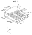
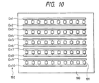
- FIG. 7 is a schematic perspective view of the display panel of an image-forming apparatus according to the invention.
- FIG. 9 is a schematic circuit diagram of a drive circuit that can be used for displaying images according to NTSC television signals as well as a block diagram of an image-forming apparatus having such a drive circuit.
- platinum and palladium of the platinum group and nickel and cobalt of the iron group provide preferable candidates.
- a second organic metal compound that can be used for the purpose of the invention like the first organic metal compound described above is expressed by chemical formula (4) below; (R 2 COO) m M ⁇ NH n R 3 k (R 1 OH) (3-n-k) ⁇ 1 where each of R 1 , R 2 and R 3 is an alkyl group having 1 to 4 carbon atoms, 1 is an integer of 2 to 4, m is an integer of 1 to 4, k is an integer of 1 to 2, n is an integer of 0 to 1 and M is a metal element.
- an organic metal complex according to the invention can be prepared by causing aminoalcohol and a metal salt of alkylcarboxylic acid to react with each other, although the number of aminoalcohol molecules to be combined with the metal can vary from 1 to 4 depending on the valence number of the metal ion.
- silver and acetic acid When, for example, silver and acetic acid are combined, silver monoacetate most typically appears.
- palladium and acetic acid are combined, palladium diacetate is most typical.
- yttrium triacetate is the most typical form that takes place when yttrium and acetic acid are combined and lead tetraacetate most typically appears as a combination of lead and acetic acid.
- Four molecules of trishydroxymethylaminomethane are coordinated with palladium acetate.
- additives that are used for preventing crystal deposition include, besides aminoalcohol, moisture-maintaining and crystallization-preventing agents such as trishydroxymethylethane, trimethyrolpropane and pentaerythritol, succharides such as glucose and sucrose and urea.
- moisture-maintaining and crystallization-preventing agents such as trishydroxymethylethane, trimethyrolpropane and pentaerythritol
- succharides such as glucose and sucrose and urea.
- succarides such as glucose and sucrose can prevent crystal deposition, they can give rise to uneven electroconductive films.
- the inventors of the present invention assumes that evaporation of the solvent of the metal-containing solution that is principally water is suppressed by the high hygroscopic property of aminoalcohol to prevent crystal deposition of the metal compound contained therein. Additionally, the ligand of the organic metal complex may be switched by the amino group of aminoalcohol and/or the vicinity of the ligand field may otherwise be affected by the amino group of aminoalcohol so that crystal deposition of the organic metal complex contained in the solution may be prevented from taking place.
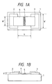
- the length W of the device electrodes is preferably between several micrometers and hundreds of several micrometers depending on the resistance of the electrodes and the electron-emitting characteristics of the device.
- the film thickness d of the device electrodes 2 and 3 is between tens of several nanometers and several micrometers.
- the emitted electric charge captured by the anode 44 (Fig. 4) is a function of the duration of time of application of the device voltage Vf. In other words, the amount of electric charge captured by the anode 44 can be effectively controlled by way of the time during which the device voltage Vf is applied.
- the interlayer insulation layer (not shown) is typically made of SiO 2 and formed on the entire surface or part of the surface of the insulating substrate 61 to show a desired contour by means of vacuum evaporation, printing or sputtering. For example, it may be formed on the entire surface or part of the surface of the substrate 61 on which the X-directional wires 62 have been formed.
- the thickness, material and manufacturing method of the interlayer insulation layer are so selected as to make it withstand the potential difference between any of the X-directional wires 62 and any of the Y-directional wire 63 observable at the crossing thereof.
- Each of the X-directional wires 62 and the Y-directional wires 63 is drawn out to form an external terminal.
- the electroconductive metal material of the wires 62 and 63, the device electrodes and the connecting wires 65 extending from the wires 62 and 63 may be same or contain a common element as an ingredient. Alternatively, they may be different from each other. These materials may be appropriately selected typically from the candidate materials listed above for the device electrodes. If the device electrodes and the connecting wires are made of a same material, they may be collectively called device electrodes without discriminating the connecting wires.
- acetone was guided into a measurement evaluation apparatus in Fig. 4, and the vacuum atmosphere of the measurement evaluation apparatus was set to be 3 x 10 -4 torr. Thereafter, activation was performed in such a manner that a voltage having a peak value of 14 V, T1 of 1 ms, and T2 of 10 ms was applied for 15 minutes. Subsequently, acetone was exhausted, and for the purpose of stabilization, the measurement evaluation apparatus was heated to 200°C and kept for 5 hours while being evacuated.
- Example 9 0.92 g of this solid and 5 g of isopropyl alcohol were dissolved in 12 g of water, and this aqueous solution was used in place of the aqueous solution for bubble jet application in Example 9. In this state, an electron-emitting device was manufactured in the same manner as in Example 9, and device characteristics were measured. At a device voltage of 14 V, a device current If was 1.7 mA, and an emission current was 0.6 ⁇ A.
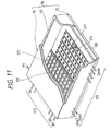
- a transparent electrode (not shown) may be formed on the outer surface of the fluorescent film 74 in the face plate 76.
- the transparent electrode is omitted.
- the gas in the glass vessel (envelope) completed as described above was exhausted by a vacuum pump through an exhaust pipe (not shown), and a sufficient degree of vacuum was obtained. Thereafter, a voltage was applied across the device electrodes 2 and 3 of the electron-emitting device 64 through out-of-vessel terminals Dox1 to Doxm and Doy1 to Doyn, and energization forming was performed to the electroconductive film 4, thereby manufacturing the electron-emitting region 5.
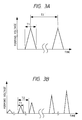
- the voltage waveform of the forming treatment is shown in Fig. 3A.
- a Ti having a thickness of 50 ⁇ and an Au film having a thickness of 5,000 ⁇ were sequentially formed by vacuum evaporation. An unnecessary portion was removed by a lift-off operation to bury the contact hole 142.
- the fluorescent film 74 consisted of only a phosphor when a monochromatic display panel was used. However, in this example, a phosphor having a stripe shape was employed. That is, black stripes were formed first, phosphors of respective colors were applied to the gap portions of the black stripes, thereby forming the fluorescent film 74. A material containing graphite as a main component ordinarily used as the material of the black stripes was used, and a slurry method was used as a method of applying the phosphor on the glass substrate 73.
- the gas in the glass vessel completed as described above was exhausted by a vacuum pump through an exhaust pipe (not shown), and a sufficient degree of vacuum was obtained. Thereafter, a voltage was applied across the device electrodes 2 and 3 of the electron-emitting device 64 through out-of-vessel terminals Dox1 to Doxm and Doy1 to Doyn, and energization forming was performed to the electron-emitting region forming thin film 4, thereby manufacturing the electron-emitting region 5.
- the voltage waveform of the forming treatment is shown in Fig. 3A.
- NAMP nickel acetate-bis(3-amino-propanol)
- Example 75 Water was added to 1.2 g of a palladium acetate-(trishydroxymethylaminomethane) complex, 0.05 g of 86% saponified poly(vinyl alcohol) (average degree of polymerization of 500), 25 g of isopropyl alcohol, and 0.8 g of diethylene glycol to prepare a palladium compound solution having a total weight of 100 g.
- the same treatment as in Example 75 was performed by using this palladium compound solution to form an electron-emitting device. After the baking step in which this device was heated at 350°C for 12 minutes, the device was observed with an optical microscope. As a result, a uniform palladium oxide film was formed without precipitating crystal.
- the electron-emitting device was estimated as an electron-emitting device, electron-emitting efficiency at a device voltage of 16 V was 0.054%.
- a metal compound solution was prepared in the same manner as in Example 78 except that trishydroxymethylaminomethane was used in place of aminomethylpropanediol.
- This metal compound solution was ejected onto a device electrode substrate by using a bubble jet printer head. When this substrate was annealed in the same manner as in Example 78, it was observed with an optical microscope that a large number of large needle crystals were precipitated in the electroconductive film. Therefore, this device was improper as an electron-emitting device.
- Supplemental example 15
- the electron-emitting region 5 formed as described above had a state wherein fine particles containing palladium element as a main component were dispersed and arranged.
- the average particle size of the fine particles was 28 ⁇ .
- Paragraph 31 A metal-containing composition for forming an electron-emitting device according to paragraph 1, wherein said organic acid group is alkylcarboxylic acid group having 1 to 5 carbon atoms.
Landscapes
- Engineering & Computer Science (AREA)
- Manufacturing & Machinery (AREA)
- Cold Cathode And The Manufacture (AREA)
Applications Claiming Priority (13)
| Application Number | Priority Date | Filing Date | Title |
|---|---|---|---|
| JP10161995 | 1995-04-04 | ||
| JP10161995A JP3229163B2 (ja) | 1995-04-04 | 1995-04-04 | 有機金属錯体、導電性膜形成用材料、並びにそれを用いた電子放出素子、電子源、表示パネルおよび画像形成装置の製造方法 |
| JP28634495A JP3217946B2 (ja) | 1995-10-09 | 1995-10-09 | 電子放出部形成用材料並びに該材料を用いた電子放出素子、電子源、表示素子及び画像形成装置の製造方法 |
| JP28634495 | 1995-10-09 | ||
| JP28816795A JP3217949B2 (ja) | 1995-10-11 | 1995-10-11 | 電子放出素子、電子源、表示素子及び画像形成装置の製造方法 |
| JP28816795 | 1995-10-11 | ||
| JP35244095 | 1995-12-28 | ||
| JP35244095A JP3217955B2 (ja) | 1995-12-28 | 1995-12-28 | 電子放出素子製造用金属組成物並びにそれを用いた電子放出素子、電子源、表示素子及び画像形成装置の製造方法 |
| JP7816496 | 1996-03-07 | ||
| JP7816496A JP3217960B2 (ja) | 1996-03-07 | 1996-03-07 | 電子放出素子形成用ニッケル錯体またはその水和物およびその溶液、並びに、電子放出素子および画像形成装置の製造方法 |
| JP10480796 | 1996-04-03 | ||
| JP10480796A JP3227090B2 (ja) | 1996-04-03 | 1996-04-03 | 電子放出素子形成用の金属含有水溶液、並びに該水溶液を用いた電子放出素子、電子源、表示パネルおよび画像形成装置の製造方法 |
| EP96302458A EP0736890B1 (de) | 1995-04-04 | 1996-04-04 | Metallenthaltende Zusammensetzung zum Bilden einer elektronenemittierenden Vorrichtung und Verfahren zur Herstellung einer elektronenemittierenden Vorrichtung, einer Elektronenquelle und eines Bilderzeugungsgerätes |
Related Parent Applications (1)
| Application Number | Title | Priority Date | Filing Date |
|---|---|---|---|
| EP96302458A Division EP0736890B1 (de) | 1995-04-04 | 1996-04-04 | Metallenthaltende Zusammensetzung zum Bilden einer elektronenemittierenden Vorrichtung und Verfahren zur Herstellung einer elektronenemittierenden Vorrichtung, einer Elektronenquelle und eines Bilderzeugungsgerätes |
Publications (1)
| Publication Number | Publication Date |
|---|---|
| EP1124247A1 true EP1124247A1 (de) | 2001-08-16 |
Family
ID=27562185
Family Applications (1)
| Application Number | Title | Priority Date | Filing Date |
|---|---|---|---|
| EP01201600A Withdrawn EP1124247A1 (de) | 1995-04-04 | 1996-04-04 | Metallenthaltende Zusammensetzung zum Erzeugen einer elektronenemittierenden Vorrichtung und Verfahren zur Herstellung einer elektronenemittierenden Vorrichtung, einer Elektronenquelle und eines Bilderzeugungsgerätes |
Country Status (1)
| Country | Link |
|---|---|
| EP (1) | EP1124247A1 (de) |
Cited By (5)
| Publication number | Priority date | Publication date | Assignee | Title |
|---|---|---|---|---|
| US6815001B1 (en) * | 1999-02-08 | 2004-11-09 | Canon Kabushiki Kaisha | Electronic device, method for producing electron source and image forming device, and apparatus for producing electronic device |
| US6896571B2 (en) | 2002-02-28 | 2005-05-24 | Canon Kabushiki Kaisha | Methods of manufacturing electron-emitting device, electron source, and image display apparatus |
| US6910936B2 (en) | 2002-02-28 | 2005-06-28 | Canon Kabushiki Kaisha | Method of transforming polymer film into carbon film in electron-emitting device |
| US6910935B2 (en) | 2002-02-28 | 2005-06-28 | Canon Kabushiki Kaisha | Methods and manufacturing electron-emitting device, electron source, and image-forming apparatus |
| US6960111B2 (en) | 2001-10-26 | 2005-11-01 | Canon Kabushiki Kaisha | Manufacturing methods for electron source and image forming apparatus |
Citations (1)
| Publication number | Priority date | Publication date | Assignee | Title |
|---|---|---|---|---|
| EP0660359A2 (de) * | 1993-12-22 | 1995-06-28 | Canon Kabushiki Kaisha | Herstellungsverfahren einer elektroemittierenden Vorrichtung und Bilderzeugungsgerät |
-
1996
- 1996-04-04 EP EP01201600A patent/EP1124247A1/de not_active Withdrawn
Patent Citations (1)
| Publication number | Priority date | Publication date | Assignee | Title |
|---|---|---|---|---|
| EP0660359A2 (de) * | 1993-12-22 | 1995-06-28 | Canon Kabushiki Kaisha | Herstellungsverfahren einer elektroemittierenden Vorrichtung und Bilderzeugungsgerät |
Cited By (6)
| Publication number | Priority date | Publication date | Assignee | Title |
|---|---|---|---|---|
| US6815001B1 (en) * | 1999-02-08 | 2004-11-09 | Canon Kabushiki Kaisha | Electronic device, method for producing electron source and image forming device, and apparatus for producing electronic device |
| US6960111B2 (en) | 2001-10-26 | 2005-11-01 | Canon Kabushiki Kaisha | Manufacturing methods for electron source and image forming apparatus |
| US6896571B2 (en) | 2002-02-28 | 2005-05-24 | Canon Kabushiki Kaisha | Methods of manufacturing electron-emitting device, electron source, and image display apparatus |
| US6910936B2 (en) | 2002-02-28 | 2005-06-28 | Canon Kabushiki Kaisha | Method of transforming polymer film into carbon film in electron-emitting device |
| US6910935B2 (en) | 2002-02-28 | 2005-06-28 | Canon Kabushiki Kaisha | Methods and manufacturing electron-emitting device, electron source, and image-forming apparatus |
| US7077716B2 (en) | 2002-02-28 | 2006-07-18 | Canon Kabushiki Kaisha | Methods of manufacturing electron-emitting device, electron source, and image display apparatus |
Similar Documents
| Publication | Publication Date | Title |
|---|---|---|
| EP0736890B1 (de) | Metallenthaltende Zusammensetzung zum Bilden einer elektronenemittierenden Vorrichtung und Verfahren zur Herstellung einer elektronenemittierenden Vorrichtung, einer Elektronenquelle und eines Bilderzeugungsgerätes | |
| US6429580B1 (en) | Methods of manufacturing electron-emitting device, electron source and image forming apparatus | |
| US6017259A (en) | Method of manufacturing electron-emitting device, electron source and image-forming apparatus | |
| KR100279304B1 (ko) | 전자원 및 이를 구비한 화상 생성 장치와, 이들의 활성화 방법 | |
| EP1124247A1 (de) | Metallenthaltende Zusammensetzung zum Erzeugen einer elektronenemittierenden Vorrichtung und Verfahren zur Herstellung einer elektronenemittierenden Vorrichtung, einer Elektronenquelle und eines Bilderzeugungsgerätes | |
| JP3229163B2 (ja) | 有機金属錯体、導電性膜形成用材料、並びにそれを用いた電子放出素子、電子源、表示パネルおよび画像形成装置の製造方法 | |
| JP3217949B2 (ja) | 電子放出素子、電子源、表示素子及び画像形成装置の製造方法 | |
| JP3217955B2 (ja) | 電子放出素子製造用金属組成物並びにそれを用いた電子放出素子、電子源、表示素子及び画像形成装置の製造方法 | |
| JP3215322B2 (ja) | 電子放出素子製造用の金属含有水溶液、それを用いた電子放出素子、電子源、表示素子および画像形成装置の製造方法 | |
| JP3258291B2 (ja) | 有機金属錯体含有インクジェットインクおよび該インクの噴射装置 | |
| JP3296549B2 (ja) | インクジェット噴射装置及びそれに用いるインクジェットインク | |
| JP3227090B2 (ja) | 電子放出素子形成用の金属含有水溶液、並びに該水溶液を用いた電子放出素子、電子源、表示パネルおよび画像形成装置の製造方法 | |
| JP3582761B2 (ja) | 電子放出部形成用有機金属化合物、並びに電子放出素子、電子源および画像形成装置の製造方法 | |
| JP3884823B2 (ja) | 電子放出素子製造用の金属化合物含有水溶液およびそれを用いた電子放出素子の製造方法 | |
| JP3592032B2 (ja) | 電子放出素子、電子源および画像形成装置の製造方法 | |
| JP3728051B2 (ja) | 電子放出素子形成用有機金属化合物、並びに電子放出素子および画像形成装置の製造方法 | |
| JP3596844B2 (ja) | 電子放出素子およびその製造方法、並びに電子源および画像形成装置 | |
| JP3587335B2 (ja) | 電子放出素子形成用有機金属化合物、並びに電子放出素子および画像形成装置の製造方法 | |
| JP3217960B2 (ja) | 電子放出素子形成用ニッケル錯体またはその水和物およびその溶液、並びに、電子放出素子および画像形成装置の製造方法 | |
| JP3217946B2 (ja) | 電子放出部形成用材料並びに該材料を用いた電子放出素子、電子源、表示素子及び画像形成装置の製造方法 | |
| JP2000204096A (ja) | 金属組成物、およびそれを用いた電子放出素子製造用金属組成物、電子放出素子の製造方法、電子放出素子および画像形成装置 | |
| JP3592030B2 (ja) | 電子放出素子製造方法並びに該電子放出素子を用いた電子源および画像形成装置の製造方法 | |
| JPH10279760A (ja) | 電子放出素子製造用金属化合物組成物、それを用いた電子放出素子の製造方法、電子放出素子および画像形成装置 | |
| JP2000204097A (ja) | 金属組成物、電子放出素子製造用金属組成物、電子放出素子製造方法、電子放出素子および画像形成装置 | |
| JPH09115432A (ja) | 電子放出素子、電子源、表示素子及び画像形成装置の製造方法 |
Legal Events
| Date | Code | Title | Description |
|---|---|---|---|
| PUAI | Public reference made under article 153(3) epc to a published international application that has entered the european phase |
Free format text: ORIGINAL CODE: 0009012 |
|
| AC | Divisional application: reference to earlier application |
Ref document number: 736890 Country of ref document: EP |
|
| AK | Designated contracting states |
Kind code of ref document: A1 Designated state(s): DE FR GB IT NL |
|
| 17P | Request for examination filed |
Effective date: 20020107 |
|
| AKX | Designation fees paid |
Free format text: DE FR GB IT NL |
|
| 17Q | First examination report despatched |
Effective date: 20050705 |
|
| STAA | Information on the status of an ep patent application or granted ep patent |
Free format text: STATUS: THE APPLICATION HAS BEEN WITHDRAWN |
|
| 18W | Application withdrawn |
Effective date: 20120612 |