EP1122810B1 - Antennenvorrichtung - Google Patents
Antennenvorrichtung Download PDFInfo
- Publication number
- EP1122810B1 EP1122810B1 EP00117315A EP00117315A EP1122810B1 EP 1122810 B1 EP1122810 B1 EP 1122810B1 EP 00117315 A EP00117315 A EP 00117315A EP 00117315 A EP00117315 A EP 00117315A EP 1122810 B1 EP1122810 B1 EP 1122810B1
- Authority
- EP
- European Patent Office
- Prior art keywords
- antenna device
- substrate
- conductor layer
- conductor
- shows
- Prior art date
- Legal status (The legal status is an assumption and is not a legal conclusion. Google has not performed a legal analysis and makes no representation as to the accuracy of the status listed.)
- Expired - Lifetime
Links
Images


Classifications
-
- H—ELECTRICITY
- H01—ELECTRIC ELEMENTS
- H01Q—ANTENNAS, i.e. RADIO AERIALS
- H01Q1/00—Details of, or arrangements associated with, antennas
- H01Q1/27—Adaptation for use in or on movable bodies
-
- H—ELECTRICITY
- H01—ELECTRIC ELEMENTS
- H01Q—ANTENNAS, i.e. RADIO AERIALS
- H01Q1/00—Details of, or arrangements associated with, antennas
- H01Q1/36—Structural form of radiating elements, e.g. cone, spiral, umbrella; Particular materials used therewith
- H01Q1/362—Structural form of radiating elements, e.g. cone, spiral, umbrella; Particular materials used therewith for broadside radiating helical antennas
-
- H—ELECTRICITY
- H01—ELECTRIC ELEMENTS
- H01Q—ANTENNAS, i.e. RADIO AERIALS
- H01Q1/00—Details of, or arrangements associated with, antennas
- H01Q1/12—Supports; Mounting means
- H01Q1/22—Supports; Mounting means by structural association with other equipment or articles
- H01Q1/24—Supports; Mounting means by structural association with other equipment or articles with receiving set
- H01Q1/241—Supports; Mounting means by structural association with other equipment or articles with receiving set used in mobile communications, e.g. GSM
- H01Q1/242—Supports; Mounting means by structural association with other equipment or articles with receiving set used in mobile communications, e.g. GSM specially adapted for hand-held use
-
- H—ELECTRICITY
- H01—ELECTRIC ELEMENTS
- H01Q—ANTENNAS, i.e. RADIO AERIALS
- H01Q1/00—Details of, or arrangements associated with, antennas
- H01Q1/36—Structural form of radiating elements, e.g. cone, spiral, umbrella; Particular materials used therewith
- H01Q1/38—Structural form of radiating elements, e.g. cone, spiral, umbrella; Particular materials used therewith formed by a conductive layer on an insulating support
Definitions
- the present invention relates to an antenna device to be used for portable communication sets.
- a linear antenna such as a pole antenna or a rod antenna
- the antenna hinders the communication set to be small size because the antenna has been attached at outside of the case of the communication set, besides causing a risk of breakage, deformation and deterioration of characteristics by suffering external mechanical forces acting on the antenna.
- the antenna is not preferable with respect to the packaging cost since a number of components are required for packaging the antenna via coaxial cables and connectors.
- Japanese Unexamined Patent Application Publication No. 9-64627 proposes a compact antenna capable of surface-packaging on a circuit board as shown in FIG. 26 .
- a helical antenna is formed within a ceramic substrate 30 by making use of a technique for forming a multi-layer ceramic substrate.
- a conductor line 31 is formed on each ceramic layer, and the conductor lines on different ceramic layers are connected one another via through holes 32 in which a conductive material is filled to form a helical conductor as a whole.
- a ceramic antenna including a helical radiation conductor is assembled by laminating the ceramic layers.
- a terminal 33 for feeding electricity to the helical conductor is provided on the side face of the substrate 30 .
- the conductor line should be designed by taking shrinkage by firing into consideration.
- a highly rigid process control is also required in order to restrict the schrinkage ratio within a prescribed range, thus making it difficult to reduce the production cost.
- conductor patterns should be nevertheless formed on at least four faces of a ceramic block having flat surfaces by a method capable of fine control of the conductor pattern such as a printing method, also preventing the production cost from being reduced.
- An antenna device according to the preamble of claim 1 is known from US-A-5,977,931 .
- the object of the present invention in view of the circumstances as hitherto described is to provide an antenna device designed to reduce the production cost.
- the present invention for attaining the object above, provides an antenna device comprising: a substrate comprising at least one of a dielectric material or a magnetic material having upper and lower faces as well as a pair of side faces on which convex portions and concave portions are alternately formed; and a helical conductor layer formed on the upper and lower faces, and on the concave portion or convex portion on a pair of the side faces of the substrate so as to spirally surround the entire substrate; and the further features recited in claim 1.
- the antenna device comprises a helical antenna in which a helical emission conductor is formed on the surface of the ceramic substrate, and the conductor layer on the upper and lower faces of the substrate can be formed by printing. Electrodes can be formed only on the convex portions by a high speed coating method such as a dip method or using a roll coater for forming the conductive layer on the convex portions on the side face. Using the roll coater enables superior mass-productivity to the printing method to be attained for forming the electrode particularly on the convex portion. It is also an advantage of forming the electrode on the convex portion that solders hardly form solder bridges when the solder is used for connecting the electrode on the convex portion in mounting the antenna device.
- the conductive layer When the conductive layer is formed in the concave portion on the side face, on the other hand, it can be formed by filling a conductor material in through holes to be described hereinafter, also offering an advantage that the solder bridge is hardly formed. Accordingly, the present invention can make mass-production easy besides enabling the production cost to be largely reduced.
- the surface mountable type antenna can be also readily manufactured since the side face convex portions and concave portions themselves on which conductor lines are formed can be utilized as terminal electrodes.
- the device comprises: a power feed electrode for feeding electricity to the helical conductor layer comprising a portion located at one end of the plural portions sequentially disposed with a given distance apart on one side face of the substrate, the plural portions constituting the helical conductor layer; an earth electrode for grounding the helical conductor layer formed at an adjoining position to the power feed electrode with a given distance apart to the power feed electrode on the same side face of the substrate as the side face on which the power feed electrode is formed; and a connection conductor layer extending from the earth electrode for connecting the earth electrode to the power feed electrode in collaboration with a part of the helical conductor layer by allowing the connection conductor layer to connect to the helical conductor layer via the upper face of the substrate.
- FIG. 1 shows a perspective view of the antenna device according to an example.
- the substrate 2 of the antenna device 1 comprises an upper face 21 and a lower face 22 , and an a pair of the side faces 23 on which concave portions 231 and convex portions 232 are alternately formed.
- Conductor layer 3 for connecting corresponding convex portions 232 one another on a pair of the side faces 23 are formed on the upper face 21 of the substrate 2 .
- Conductor layers 4 for connecting the convex portions 232 on a pair of the side faces 23 , one on the side face and the other on the opposite side face that is shifted by one pitch from the former one, are formed on the lower face 22 of the substrate 2 .
- Conductor layers 5 are also formed on the convex portions 232 of a pair of the side faces 23 , and these conductor layers 3 , 4 and 5 serve as a helical conductor layer for surrounding the substrate 2 as a whole.
- the preferable substrate 2 has a stable specific dielectric constant ( ⁇ r) or a stable specific magnetic permeability ( ⁇ r) with a low loss and a small temperature coefficient ( ⁇ r) of the resonance frequency.
- ⁇ r alumina based ceramic
- the preferable conductor comprises a low resistance conductor such as copper, silver and gold.
- a silver-platinum paste (QS-171 made by Dupont CO.) was used in this example.
- FIGS. 2 to 5 showing the manufacturing process of the antenna device 1 shown in FIG. 1 .
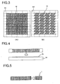
- An alumina substrate 9 shown in FIG. 2 is firstly prepared. Snap lines 10 are provided on the alumina substrate 9 so as to be able to divide the substrate into a desired size in the steps hereinafter. Through holes 11 are also provided at desired sites on the snap lines.
- the snap lines 10 were disposed by a distance of 5 mm apart along the vertical direction and by a distance of 10 mm apart along the transverse direction, and the through holes 11 with a diameter of 0.8 mm were disposed by a distance of 2 mm apart on the snap lines along the transverse direction on the alumina substrate with a width of 50 mm, a length of 50 mm and a thickness of 1 mm.
- conductor patterns 12 and 13 as shown in FIG. 3A and FIG. 3B were formed on the upper face 91 and lower face 92 , respectively, of the alumina substrate 9 .
- the patterns were formed by screen-printing a conductive paste to subject the pattern to firing at 850°C after drying.
- the alumina substrate 9 after forming the upper and lower conductors were divided along the snap lines on which the through holes had been formed as shown in FIG. 4 .
- a conductor paste 15 to a thickness of about 0.2 mm on a flat plate 14 such as a glass plate using a squeezer, convex portions formed on the alumina substrate by the through holes were dipped into the conductor paste 15 to coat only the tips of the convex portions with the conductor paste 15 followed by drying and firing.
- an antenna device 1 was finally obtained by dividing the flat plate into minimum units along the snap line. A lot of the antennas having such construction as described above can be manufactured at a time to enable a cost reduction effect to be exhibited.
- FIG. 6 shows a perspective view of the antenna device according to another example.
- the substrate 2 of this antenna device 1 comprises an upper face 21 , a lower face 22 and a pair of side faces 23 on which concave portions 231 and convex portions 232 are alternately formed as in the substrate 2 of the antenna device 1 shown in FIG. 1 .
- the conductor layer of the antenna device 1 shown in FIG. 6 is a little different from the conductor layer of the antenna device shown in FIG. 1 .
- the conductor layer 3 for connecting between a pair of the concave portions 231 with each other is formed on the upper face 21
- the conductor layer 4 for connecting one concave portion to the other concave portion that is shifted by one pitch from the former one is formed on the back face 22
- the conductor layer 5 is formed on the inner wall face of the concave portion, thereby forming a helical conductor layer with the conductor layers 3 , 4 and 5 .
- these conductor layers 3 , 4 and 5 also serve as a helical conductor layer for surrounding the substrate 2 as a whole, as in the antenna device shown in FIG. 1 .
- the preferable substrate 2 of the antenna device 1 shown in FIG. 6 also has a stable specific dielectric constant ( ⁇ r) or a stable specific magnetic permeability ( ⁇ r) with a low loss and a small temperature coefficient ( ⁇ r) of the resonance frequency, as in the antenna device shown in FIG. 1 .
- the preferable conductor comprises a low resistance conductor such as copper, silver and gold.
- a silver-platinum paste (QS-171 made by Dupont CO.) was used in this example.
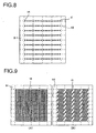
- FIGS. 7 to 10 showing the manufacturing process of the antenna device 1 shown in FIG. 6 .
- Snap lines 10 are provided on the alumina substrate 9 as shown in FIG. 7 so as to be able to divide the substrate into a desired size in the steps hereinafter.
- Through holes 11 are also provided at desired sites on the snap lines.
- the snap lines 10 were disposed by a distance of 5 mm apart along the vertical direction and by a distance of 10 mm apart along the transverse direction, and the through holes 11 with a diameter of 0.8 mm were disposed by a distance of 2 mm apart on the snap lines along the transverse direction on the alumina substrate 9 with a width of 50 mm, a length of 50 mm and a thickness of 1 mm.
- the paste was fired at 850°C after drying to complete through hole conductors 14 .
- conductor patterns 12 and 13 were formed by printing as shown in FIG. 9A and FIG. 9B , respectively, on the upper face 91 and lower face 92 of the alumina substrate 9 .
- the antenna device 1 is finally obtained by dividing the substrate into minimum units along the snap lines 10 as shown in FIG. 10 .
- a lot of the antennae having such construction as described above can be manufactured at a time to enable a cost reduction effect to be exhibited.
- a layer having the same quality as the alumina substrate 9 may be formed on the conductor layer formed on the alumina substrate before or after dividing the alumina substrate 9 in either of these examples, thereby allowing an antenna for use in the same transmission and reception band to be more compacted.
- the performance of the antenna device manufactured as described above will be described hereinafter.
- the antenna device shown in FIG. 1 will be explained herein.
- the antenna device 1 was mounted on a evaluation substrate with a length of 25 mm, a width of 50 mm and a thickness of 0.8 mm as shown in FIG. 11 .
- a strip line 17 and a ground face 18 are formed on the surface and back face of the insulation substrate 16 in this evaluation substrate. Electricity is supplied from a SMA connector 19 at one end to the antenna device 1 at the other end via the strip line 17.
- the resonance frequency was 2448 MHz and the reflection loss was -6 dM or below at a band width of 133MHz.
- the radiation pattern on the XY plane in FIG. 11 is shown in FIG. 13 .
- Radiation gain turned out to be approximately omnidirectional in this face, while the maximum gain was -0.7 dBi and the minimum gain was -2.3 dBi.
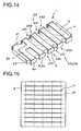
- FIG. 14 shows a perspective view of an antenna device according to an embodiment of the present invention.
- the substrate 2 of the antenna device 1 comprises an upper face 21 and a lower face 22 , and a pair of side faces 23 on which concave portions 231 and convex portions 232 are alternately formed.
- Conductor layers 3 for connecting between corresponding two convex portions 232 on a pair of the side faces 23 are formed on the upper face 21 of the substrate 2 .
- Conductor layers 4 for connecting the convex portions 232 on a pair of the side faces 23 , one on the side face and the other on the opposite side face that is shifted by one pitch from the former one, are formed on the lower face 22 of the substrate 2 .
- Conductor layers 5 are also formed on the concave portions 232 on a pair of side faces 23 , and these conductor layers 3 , 4 and 5 serve as a helical conductor layer spirally surrounding the substrate 2 as a whole.
- the conductor layer at the most end of the conductor layers constituting the helical conductor layer, spirally surrounding the substrate as a whole, of the conductor layers 5 on one side face 23a of a pair of the side faces 23 serves as a power feed electrode 5a .
- a ground electrode 6a is formed at the adjoining position to the power feed electrode 5a with a given distance apart from the helical conductor layer.
- a connection conductor 6b connecting the helical conductor layer to the ground electrode 6a via the upper face of the substrate is additionally formed.
- the preferable substrate 2 has a stable specific dielectric constant ( ⁇ r) or a stable specific magnetic permeability ( ⁇ r) with a low loss and a small temperature coefficient ( ⁇ r) of the resonance frequency.
- ⁇ r alumina based ceramic
- the preferable conductor comprises a low resistance conductor such as copper, silver and gold.
- a silver-platinum paste (QS-171 made by Dupont CO.) was used in this example.
- FIGS. 15 to 19 showing the method for manufacturing the antenna device 1 shown in FIG. 14 .
- An alumina substrate 9 as shown in FIG. 15 is firstly prepared. Snap lines 10 are provided on this alumina substrate 9 so that it can be divided into a desired size in the subsequent steps. Through holes 11 are also provided on the desired sites on the snap line.
- the snap lines 10 were disposed by a distance of 5 mm apart along the vertical direction and by a distance of 10 mm apart along the transverse direction, and the through holes 11 with a diameter of 0.8 mm were disposed by a distance of 2 mm apart on the snap lines along the vertical direction on the alumina substrate 9 with a width of 50 mm, a length of 50 mm and a thickness of 1 mm.
- Conductor patterns 12 and 13 were then formed on the upper face 91 and lower face 92 , respectively, on the alumina substrate 9 as shown in FIGS> 16 and 17.
- a conductor paste was screen-printed for forming the conductor patterns, followed by firing at 850°C after drying.
- the alumina substrate 9 after forming the upper and lower conductors was divided along the snap lines on which the through holes had been formed as shown in FIG. 18 .
- a conductor paste 15 was spread to a thickness of about 0.2 mm on a flat plate 14 such as a glass plate using a squeezer, convex portions formed on the alumina substrate by the through holes were dipped into the conductor paste 15 to coat only the tips of the convex portions with the conductor paste 15 followed by drying and firing.
- An antenna device 1 was finally obtained by dividing the substrate into minimum units along the snap lines. A lot of the antennas having such construction as described above can be manufactured at a time to enable a cost reduction effect to be exhibited.
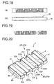
- FIG. 20 shows a perspective view of the antenna device according to an example not part of the present invention. The difference of this example from the embodiment shown in FIG. 14 will be described hereinafter. While the ground electrode 6a is connected to the conductor layer spirally surrounding the substrate as a whole via the connection conductor 6b on the upper face of the substrate in the third embodiment shown in FIG. 14 , the ground electrode 6a is connected to the conductor layer via the connection conductor 6b on the opposed side face 23b to the side face 23a on which the ground electrode 6a is formed in the example shown in FIG. 20 .
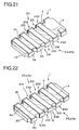
- FIG. 21 shows a perspective view of an antenna device according to an example.
- a conductor layer at the most end of the conductor layers constituting the helical conductor layer, spirally surrounding the substrate as a whole, of plural conductor layers 5 disposed on one side face 23a serves as a ground electrode 5b , which also serves as a ground conductor, and the conductor layer adjoining to the ground electrode serves as a power feed electrode 5a .
- FIG. 22 shows a perspective view on an another example of the antenna device.
- antenna device itself shown in FIG. 22 is provided as a comparative example of the antenna device, it also serves as an antenna device for constituting an assembly of the antenna device to be described hereinafter.
- the ground electrode 6a is connected to the helical conductor layer surrounding the substrate as a whole with a connection conductor 6b , via the upper face of the substrate, via the side face 23b at the opposite side to the side face 23a on which the ground electrode 6a is formed, and via the lower face of the substrate.
- the antenna device 1 was mounted on an evaluation substrate with a width of 50 mm, a length of 25 mm and a thickness of 0.8 mm as shown in FIG. 23 .
- a strip line 17 is formed on the surface, and a ground face 18 is formed on the back face of the insulation substrate 16 , and electricity is supplied from a SAM connector 19 trough the strip line 17 to the antenna device 1 mounted on the other end of the substrate.
- TABLE 1 shows the results measured as described above.
- the "3 ⁇ value of dispersion” denotes the 3 ⁇ value of dispersion of the resonance frequencies when a number of the antenna devices having the same specification one another are manufactured.
- TABLE 1 DISPERSION OF RESONANCE FREQUENCY FROM CENTRAL FREQUENCY 2.45 GHz CONTACT POSITION 3 ⁇ VALUE OF DISPERSION EXAMPLE 1: UPPER FAXE OF ANTENNA ( FIG. 14 ) ⁇ 30MHz
- EXAMPLE 2 SIDE FACE ( FIG. 20 ) ⁇ 60MHz
- EXAMPLE 3 TERMINAL ALSO SERVES AS CONTACT POSITION 21) ⁇ 62MHz COMPARATIVE EXAMPLE: FACE ( FIG.22 ) ⁇ 155MHz
- TABLE 1 shows that the distribution is suppressed in Examples 1 to 3 as compared with Comparative Example.
- FIG. 24 shows an assembly of the antenna device according to the first example described above.
- FIG. 24 shows a circuit board 97 viewed from the bottom face on which the antenna device 1 is mounted so that the lower face of the antenna device contacts the upper face of the substrate.
- the ground electrode shown in FIG. 22 is connected to the helical conductor layer via the connection conductor layer on the lower face of the substrate in this type of the antenna device 1 .
- a hole 97a piercing from the upper face to the lower face is provided on the circuit board 97 by chipping a part of the circuit board.
- the contact point between the connection conductor layer and the helical conductor layer on the lower face of the substrate of the antenna device 1 is just located on the hole 97a to avoid the connection part from contacting to the circuit board 97 .
- FIG. 25 shows an another assembly of the antenna device according to the second example described above.
- FIG. 25 also shows a circuit board 97 viewed from the bottom face on which the antenna device 1 of the type shown in FIG. 22 is mounted so that the lower face of the antenna device contact the upper face of the substrate as in FIG. 22 .
- the contact portion between the connection conductor and the helical conductor of the antenna device 1 is made to protrude from the circuit board 97 .
- Dispersion of the resonance frequencies can be suppressed by mounting the antenna device so that a part of the circuit board is chipped or the contact portion is allowed to protrude from the circuit board, even when the contact portion is formed on the lower face of the antenna device.
- TABLE 2 shows the results of measurement of the dispersion of resonance frequencies of the assembly of the antenna device in the examples shown in FIGS. 24 and 25 .
- TABLE 2 DISPERSION OF RESONANCE FREQUENCY FROM CENTRAL FREQUENCY 2.45 GHz MOUNTING METHOD 3 ⁇ VALUE OF DISPERSION CHIPPING OF SUBSTRATE UNDER CONTACT POINT ( FIG. 24 ) ⁇ 72MHz PROTRUSION OF ANTENNA ( FIG. 25 ) ⁇ 68MHz
- TABLE 2 shows that the dispersions of frequencies in this table are smaller as compared with the dispersion in the lowermost row in TABLE 1.
Landscapes
- Engineering & Computer Science (AREA)
- Computer Networks & Wireless Communication (AREA)
- Details Of Aerials (AREA)
- Support Of Aerials (AREA)
Claims (1)
- Antennenvorrichtung (1) mit:einem Substrat (2), das zumindest entweder ein dielektrisches Material oder ein magnetisches Material aufweist und eine obere (21) und eine untere Fläche (22) sowie ein Paar Seitenfläche (23) umfasst, an denen konvexe Abschnitte (232) und konkave Abschnitte (231) abwechselnd ausgebildet sind, undeine spiralenförmige Leiterschicht (3, 4, 5), die an der oberen (21) und unteren Fläche (22) und am konkaven Abschnitt (231) oder konvexen Abschnitt (232) am Paar der Seitenflächen (23) des Substrats (2) so ausgebildet ist, dass sie das gesamte Substrat (2) spiralförmig umgibt,gekennzeichnet durch
eine Energiezuführelektrode (5a) zum Zuführen von Elektrizität zur spiralenförmigen Leiterschicht (3, 4, 5), wobei die Energiezuführelektrode (5a) einen Abschnitt aufweist, der an einem Ende mehrerer Abschnitte gelegen ist, die in einem bestimmten Abstand getrennt an einer Seitenfläche (23) des Substrats (2) nacheinander angeordnet sind, wobei die mehreren Abschnitte die spiralenförmige Leiterschicht (3, 4, 5) bilden,
eine Erdungselektrode (6a) zum Erden der spiralenförmigen Leiterschicht (3, 4, 5), wobei die Erdungselektrode (6a) an einer angrenzenden Position zur Energiezuführelektrode (5a) mit einem bestimmten Abstand getrennt zur Energiezuführelektrode (5a) an der gleichen Seitenfläche (23) des Substrats (2) wie der Seitenfläche (23) ausgebildet ist, an der die Energiezuführelektrode (5a) ausgebildet ist, und
eine Verbindungsleiterschicht (6b), die sich von der Erdungselektrode (6a) zum Verbinden der Erdungselektrode (6a) mit der Energiezuführelektrode (5a) in Zusammenwirkung mit einem Teil der spiralenförmigen Leiterschicht (3, 4, 5) durch Verbinden der Verbindungsleiterschicht (6b) über die obere Fläche (21) des Substrats (2) mit der spiralenförmigen Leiterschicht (3, 4, 5) erstreckt.
Applications Claiming Priority (2)
| Application Number | Priority Date | Filing Date | Title |
|---|---|---|---|
| JP2000027222 | 2000-01-31 | ||
| JP2000027222A JP3178469B2 (ja) | 1999-02-25 | 2000-01-31 | アンテナ装置およびアンテナ装置組立体 |
Publications (3)
| Publication Number | Publication Date |
|---|---|
| EP1122810A2 EP1122810A2 (de) | 2001-08-08 |
| EP1122810A3 EP1122810A3 (de) | 2004-04-21 |
| EP1122810B1 true EP1122810B1 (de) | 2012-02-22 |
Family
ID=18552820
Family Applications (1)
| Application Number | Title | Priority Date | Filing Date |
|---|---|---|---|
| EP00117315A Expired - Lifetime EP1122810B1 (de) | 2000-01-31 | 2000-08-18 | Antennenvorrichtung |
Country Status (4)
| Country | Link |
|---|---|
| US (1) | US6486852B1 (de) |
| EP (1) | EP1122810B1 (de) |
| KR (1) | KR100702088B1 (de) |
| CN (1) | CN1277333C (de) |
Families Citing this family (10)
| Publication number | Priority date | Publication date | Assignee | Title |
|---|---|---|---|---|
| US6897823B2 (en) * | 2001-07-31 | 2005-05-24 | Hitachi Maxell, Ltd. | Plane antenna and method for manufacturing the same |
| CN102683839A (zh) * | 2003-12-25 | 2012-09-19 | 三菱综合材料株式会社 | 天线装置 |
| KR100765959B1 (ko) * | 2005-01-11 | 2007-10-11 | 영인프런티어(주) | 휴대폰용 내장 안테나 제조방법 |
| KR100691162B1 (ko) * | 2005-05-16 | 2007-03-09 | 삼성전기주식회사 | 직교 헬리컬 안테나 |
| JP4688068B2 (ja) * | 2006-06-29 | 2011-05-25 | 三菱マテリアル株式会社 | アンテナ装置 |
| US8248323B2 (en) * | 2008-05-30 | 2012-08-21 | Motorola Solutions, Inc. | Antenna and method of forming same |
| JP5068829B2 (ja) * | 2010-01-26 | 2012-11-07 | 日本写真印刷株式会社 | アンテナ付射出成形同時加飾品およびその製造方法、ならびにアンテナ付筐体の給電構造 |
| CN107546490A (zh) * | 2016-06-27 | 2018-01-05 | 上海光线新材料科技有限公司 | 一种基于磁性材料的天线模组及其制造方法 |
| TWI750492B (zh) * | 2019-07-31 | 2021-12-21 | 台灣禾邦電子有限公司 | 旋繞共振式天線 |
| CN112350052A (zh) * | 2019-08-06 | 2021-02-09 | 台湾禾邦电子有限公司 | 一种旋绕共振式天线 |
Citations (3)
| Publication number | Priority date | Publication date | Assignee | Title |
|---|---|---|---|---|
| US2781514A (en) * | 1953-04-29 | 1957-02-12 | Itt | Helical antenna system |
| GB784807A (en) * | 1954-08-21 | 1957-10-16 | Philips Electrical Ind Ltd | Improvements in or relating to aerials |
| US2866197A (en) * | 1953-03-20 | 1958-12-23 | Itt | Tuned antenna system |
Family Cites Families (15)
| Publication number | Priority date | Publication date | Assignee | Title |
|---|---|---|---|---|
| DE1439264A1 (de) * | 1963-07-24 | 1968-10-24 | Siemens Ag | Verfahren zum Herstellen einer mehrere Windungen aufweisenden Spule |
| JPH04137602A (ja) | 1990-09-28 | 1992-05-12 | Toshiba Lighting & Technol Corp | チップコイル |
| JP3317522B2 (ja) | 1992-07-06 | 2002-08-26 | 原田工業株式会社 | 衛星通信用ヘリカルアンテナ |
| EP0658907A1 (de) * | 1993-12-14 | 1995-06-21 | Antenna Products Limited | Verfahren zur Herstellung elektrischer Komponenten |
| JPH0936639A (ja) | 1995-05-17 | 1997-02-07 | Murata Mfg Co Ltd | チップアンテナ |
| JPH0993021A (ja) * | 1995-09-25 | 1997-04-04 | Murata Mfg Co Ltd | チップアンテナ |
| US5696517A (en) * | 1995-09-28 | 1997-12-09 | Murata Manufacturing Co., Ltd. | Surface mounting antenna and communication apparatus using the same |
| JPH09214227A (ja) * | 1996-02-07 | 1997-08-15 | Murata Mfg Co Ltd | チップアンテナ |
| JP3146994B2 (ja) | 1996-08-22 | 2001-03-19 | 株式会社村田製作所 | アンテナ及びその共振周波数調整方法 |
| JP3093650B2 (ja) | 1996-09-06 | 2000-10-03 | 埼玉日本電気株式会社 | ヘリカルアンテナ |
| JPH10208942A (ja) | 1997-01-17 | 1998-08-07 | Citizen Electron Co Ltd | 磁芯入りチップインダクタとその製造方法 |
| JPH10247808A (ja) * | 1997-03-05 | 1998-09-14 | Murata Mfg Co Ltd | チップアンテナ及びその周波数調整方法 |
| US5977931A (en) * | 1997-07-15 | 1999-11-02 | Antenex, Inc. | Low visibility radio antenna with dual polarization |
| JP3296276B2 (ja) * | 1997-12-11 | 2002-06-24 | 株式会社村田製作所 | チップアンテナ |
| US6288680B1 (en) * | 1998-03-18 | 2001-09-11 | Murata Manufacturing Co., Ltd. | Antenna apparatus and mobile communication apparatus using the same |
-
2000
- 2000-08-17 KR KR1020000047485A patent/KR100702088B1/ko active IP Right Grant
- 2000-08-18 EP EP00117315A patent/EP1122810B1/de not_active Expired - Lifetime
- 2000-08-21 US US09/641,702 patent/US6486852B1/en not_active Expired - Lifetime
- 2000-10-05 CN CNB001342355A patent/CN1277333C/zh not_active Expired - Lifetime
Patent Citations (3)
| Publication number | Priority date | Publication date | Assignee | Title |
|---|---|---|---|---|
| US2866197A (en) * | 1953-03-20 | 1958-12-23 | Itt | Tuned antenna system |
| US2781514A (en) * | 1953-04-29 | 1957-02-12 | Itt | Helical antenna system |
| GB784807A (en) * | 1954-08-21 | 1957-10-16 | Philips Electrical Ind Ltd | Improvements in or relating to aerials |
Also Published As
| Publication number | Publication date |
|---|---|
| KR20010077847A (ko) | 2001-08-20 |
| CN1307379A (zh) | 2001-08-08 |
| KR100702088B1 (ko) | 2007-04-02 |
| EP1122810A3 (de) | 2004-04-21 |
| CN1277333C (zh) | 2006-09-27 |
| US6486852B1 (en) | 2002-11-26 |
| EP1122810A2 (de) | 2001-08-08 |
Similar Documents
| Publication | Publication Date | Title |
|---|---|---|
| US6323824B1 (en) | Dielectric resonator antenna | |
| EP0923153B1 (de) | Chipantenne | |
| US6023251A (en) | Ceramic chip antenna | |
| CA2200675C (en) | A printed antenna structure for wireless data communications | |
| US20040108957A1 (en) | Pattern antenna | |
| JPH05327331A (ja) | プリントアンテナ | |
| US5627551A (en) | Antennas for surface mounting and method of adjusting frequency thereof | |
| KR101027089B1 (ko) | 표면실장형 안테나 및 안테나 장치 | |
| JP3206825B2 (ja) | プリントアンテナ | |
| US6958728B2 (en) | Flat antenna | |
| EP1122810B1 (de) | Antennenvorrichtung | |
| EP1517400B1 (de) | SMD Antenne | |
| JP2002185241A (ja) | マイクロ波レンジ用パッチアンテナ | |
| EP0812030A1 (de) | Chip Antenne | |
| WO1999027607A2 (en) | Antenna structure | |
| CN112821050A (zh) | 天线组件及电子设备 | |
| GB2283131A (en) | Antenna | |
| KR20020065811A (ko) | 전자결합 인쇄 슬롯 마이크로스트립 안테나 | |
| JP3042386B2 (ja) | 表面実装型アンテナおよびこれを用いた通信機 | |
| KR100442053B1 (ko) | 적층 구조를 갖는 칩 안테나 | |
| JP3758495B2 (ja) | アンテナ装置及びアンテナ装置の製造方法 | |
| US6727852B2 (en) | Dual band microstrip antenna | |
| JP3178469B2 (ja) | アンテナ装置およびアンテナ装置組立体 | |
| JP3042384B2 (ja) | 表面実装型アンテナおよびこれを用いた通信機 | |
| CN218482382U (zh) | 一种可扩展的介质谐振器、天线模组及电子设备 |
Legal Events
| Date | Code | Title | Description |
|---|---|---|---|
| PUAI | Public reference made under article 153(3) epc to a published international application that has entered the european phase |
Free format text: ORIGINAL CODE: 0009012 |
|
| AK | Designated contracting states |
Kind code of ref document: A2 Designated state(s): AT BE CH CY DE DK ES FI FR GB GR IE IT LI LU MC NL PT SE |
|
| AX | Request for extension of the european patent |
Free format text: AL;LT;LV;MK;RO;SI |
|
| PUAL | Search report despatched |
Free format text: ORIGINAL CODE: 0009013 |
|
| AK | Designated contracting states |
Kind code of ref document: A3 Designated state(s): AT BE CH CY DE DK ES FI FR GB GR IE IT LI LU MC NL PT SE |
|
| AX | Request for extension of the european patent |
Extension state: AL LT LV MK RO SI |
|
| 17P | Request for examination filed |
Effective date: 20040727 |
|
| 17Q | First examination report despatched |
Effective date: 20040826 |
|
| AKX | Designation fees paid |
Designated state(s): DE FI FR GB SE |
|
| 17Q | First examination report despatched |
Effective date: 20040826 |
|
| GRAP | Despatch of communication of intention to grant a patent |
Free format text: ORIGINAL CODE: EPIDOSNIGR1 |
|
| RTI1 | Title (correction) |
Free format text: ANTENNA DEVICE |
|
| RTI1 | Title (correction) |
Free format text: ANTENNA DEVICE |
|
| GRAS | Grant fee paid |
Free format text: ORIGINAL CODE: EPIDOSNIGR3 |
|
| GRAA | (expected) grant |
Free format text: ORIGINAL CODE: 0009210 |
|
| AK | Designated contracting states |
Kind code of ref document: B1 Designated state(s): DE FI FR GB SE |
|
| REG | Reference to a national code |
Ref country code: GB Ref legal event code: FG4D |
|
| RAP2 | Party data changed (patent owner data changed or rights of a patent transferred) |
Owner name: MITSUBISHI MATERIALS CORPORATION |
|
| REG | Reference to a national code |
Ref country code: SE Ref legal event code: TRGR |
|
| REG | Reference to a national code |
Ref country code: DE Ref legal event code: R096 Ref document number: 60046943 Country of ref document: DE Effective date: 20120412 |
|
| PLBE | No opposition filed within time limit |
Free format text: ORIGINAL CODE: 0009261 |
|
| STAA | Information on the status of an ep patent application or granted ep patent |
Free format text: STATUS: NO OPPOSITION FILED WITHIN TIME LIMIT |
|
| 26N | No opposition filed |
Effective date: 20121123 |
|
| REG | Reference to a national code |
Ref country code: DE Ref legal event code: R097 Ref document number: 60046943 Country of ref document: DE Effective date: 20121123 |
|
| REG | Reference to a national code |
Ref country code: FR Ref legal event code: PLFP Year of fee payment: 17 |
|
| REG | Reference to a national code |
Ref country code: FR Ref legal event code: PLFP Year of fee payment: 18 |
|
| REG | Reference to a national code |
Ref country code: FR Ref legal event code: PLFP Year of fee payment: 19 |
|
| PGFP | Annual fee paid to national office [announced via postgrant information from national office to epo] |
Ref country code: FI Payment date: 20190822 Year of fee payment: 20 Ref country code: SE Payment date: 20190821 Year of fee payment: 20 Ref country code: FR Payment date: 20190822 Year of fee payment: 20 Ref country code: DE Payment date: 20190822 Year of fee payment: 20 |
|
| PGFP | Annual fee paid to national office [announced via postgrant information from national office to epo] |
Ref country code: GB Payment date: 20190821 Year of fee payment: 20 |
|
| REG | Reference to a national code |
Ref country code: DE Ref legal event code: R071 Ref document number: 60046943 Country of ref document: DE |
|
| REG | Reference to a national code |
Ref country code: GB Ref legal event code: PE20 Expiry date: 20200817 |
|
| REG | Reference to a national code |
Ref country code: FI Ref legal event code: MAE |
|
| REG | Reference to a national code |
Ref country code: SE Ref legal event code: EUG |
|
| PG25 | Lapsed in a contracting state [announced via postgrant information from national office to epo] |
Ref country code: GB Free format text: LAPSE BECAUSE OF EXPIRATION OF PROTECTION Effective date: 20200817 |