EP1118902A1 - Flüssigkristallanzeigevorrichtung - Google Patents
Flüssigkristallanzeigevorrichtung Download PDFInfo
- Publication number
- EP1118902A1 EP1118902A1 EP00949917A EP00949917A EP1118902A1 EP 1118902 A1 EP1118902 A1 EP 1118902A1 EP 00949917 A EP00949917 A EP 00949917A EP 00949917 A EP00949917 A EP 00949917A EP 1118902 A1 EP1118902 A1 EP 1118902A1
- Authority
- EP
- European Patent Office
- Prior art keywords
- liquid crystal
- light
- display element
- crystal display
- substrate
- Prior art date
- Legal status (The legal status is an assumption and is not a legal conclusion. Google has not performed a legal analysis and makes no representation as to the accuracy of the status listed.)
- Withdrawn
Links
Images






Classifications
-
- G—PHYSICS
- G02—OPTICS
- G02F—OPTICAL DEVICES OR ARRANGEMENTS FOR THE CONTROL OF LIGHT BY MODIFICATION OF THE OPTICAL PROPERTIES OF THE MEDIA OF THE ELEMENTS INVOLVED THEREIN; NON-LINEAR OPTICS; FREQUENCY-CHANGING OF LIGHT; OPTICAL LOGIC ELEMENTS; OPTICAL ANALOGUE/DIGITAL CONVERTERS
- G02F1/00—Devices or arrangements for the control of the intensity, colour, phase, polarisation or direction of light arriving from an independent light source, e.g. switching, gating or modulating; Non-linear optics
- G02F1/01—Devices or arrangements for the control of the intensity, colour, phase, polarisation or direction of light arriving from an independent light source, e.g. switching, gating or modulating; Non-linear optics for the control of the intensity, phase, polarisation or colour
- G02F1/13—Devices or arrangements for the control of the intensity, colour, phase, polarisation or direction of light arriving from an independent light source, e.g. switching, gating or modulating; Non-linear optics for the control of the intensity, phase, polarisation or colour based on liquid crystals, e.g. single liquid crystal display cells
- G02F1/133—Constructional arrangements; Operation of liquid crystal cells; Circuit arrangements
- G02F1/1333—Constructional arrangements; Manufacturing methods
- G02F1/1335—Structural association of cells with optical devices, e.g. polarisers or reflectors
-
- G—PHYSICS
- G02—OPTICS
- G02F—OPTICAL DEVICES OR ARRANGEMENTS FOR THE CONTROL OF LIGHT BY MODIFICATION OF THE OPTICAL PROPERTIES OF THE MEDIA OF THE ELEMENTS INVOLVED THEREIN; NON-LINEAR OPTICS; FREQUENCY-CHANGING OF LIGHT; OPTICAL LOGIC ELEMENTS; OPTICAL ANALOGUE/DIGITAL CONVERTERS
- G02F1/00—Devices or arrangements for the control of the intensity, colour, phase, polarisation or direction of light arriving from an independent light source, e.g. switching, gating or modulating; Non-linear optics
- G02F1/01—Devices or arrangements for the control of the intensity, colour, phase, polarisation or direction of light arriving from an independent light source, e.g. switching, gating or modulating; Non-linear optics for the control of the intensity, phase, polarisation or colour
- G02F1/13—Devices or arrangements for the control of the intensity, colour, phase, polarisation or direction of light arriving from an independent light source, e.g. switching, gating or modulating; Non-linear optics for the control of the intensity, phase, polarisation or colour based on liquid crystals, e.g. single liquid crystal display cells
- G02F1/133—Constructional arrangements; Operation of liquid crystal cells; Circuit arrangements
- G02F1/1333—Constructional arrangements; Manufacturing methods
- G02F1/1335—Structural association of cells with optical devices, e.g. polarisers or reflectors
- G02F1/133502—Antiglare, refractive index matching layers
-
- G—PHYSICS
- G02—OPTICS
- G02F—OPTICAL DEVICES OR ARRANGEMENTS FOR THE CONTROL OF LIGHT BY MODIFICATION OF THE OPTICAL PROPERTIES OF THE MEDIA OF THE ELEMENTS INVOLVED THEREIN; NON-LINEAR OPTICS; FREQUENCY-CHANGING OF LIGHT; OPTICAL LOGIC ELEMENTS; OPTICAL ANALOGUE/DIGITAL CONVERTERS
- G02F1/00—Devices or arrangements for the control of the intensity, colour, phase, polarisation or direction of light arriving from an independent light source, e.g. switching, gating or modulating; Non-linear optics
- G02F1/01—Devices or arrangements for the control of the intensity, colour, phase, polarisation or direction of light arriving from an independent light source, e.g. switching, gating or modulating; Non-linear optics for the control of the intensity, phase, polarisation or colour
- G02F1/13—Devices or arrangements for the control of the intensity, colour, phase, polarisation or direction of light arriving from an independent light source, e.g. switching, gating or modulating; Non-linear optics for the control of the intensity, phase, polarisation or colour based on liquid crystals, e.g. single liquid crystal display cells
- G02F1/133—Constructional arrangements; Operation of liquid crystal cells; Circuit arrangements
- G02F1/1333—Constructional arrangements; Manufacturing methods
- G02F1/1335—Structural association of cells with optical devices, e.g. polarisers or reflectors
- G02F1/133509—Filters, e.g. light shielding masks
- G02F1/133512—Light shielding layers, e.g. black matrix
-
- G—PHYSICS
- G02—OPTICS
- G02F—OPTICAL DEVICES OR ARRANGEMENTS FOR THE CONTROL OF LIGHT BY MODIFICATION OF THE OPTICAL PROPERTIES OF THE MEDIA OF THE ELEMENTS INVOLVED THEREIN; NON-LINEAR OPTICS; FREQUENCY-CHANGING OF LIGHT; OPTICAL LOGIC ELEMENTS; OPTICAL ANALOGUE/DIGITAL CONVERTERS
- G02F1/00—Devices or arrangements for the control of the intensity, colour, phase, polarisation or direction of light arriving from an independent light source, e.g. switching, gating or modulating; Non-linear optics
- G02F1/01—Devices or arrangements for the control of the intensity, colour, phase, polarisation or direction of light arriving from an independent light source, e.g. switching, gating or modulating; Non-linear optics for the control of the intensity, phase, polarisation or colour
- G02F1/13—Devices or arrangements for the control of the intensity, colour, phase, polarisation or direction of light arriving from an independent light source, e.g. switching, gating or modulating; Non-linear optics for the control of the intensity, phase, polarisation or colour based on liquid crystals, e.g. single liquid crystal display cells
- G02F1/133—Constructional arrangements; Operation of liquid crystal cells; Circuit arrangements
- G02F1/136—Liquid crystal cells structurally associated with a semi-conducting layer or substrate, e.g. cells forming part of an integrated circuit
- G02F1/1362—Active matrix addressed cells
- G02F1/136209—Light shielding layers, e.g. black matrix, incorporated in the active matrix substrate, e.g. structurally associated with the switching element
-
- G—PHYSICS
- G02—OPTICS
- G02F—OPTICAL DEVICES OR ARRANGEMENTS FOR THE CONTROL OF LIGHT BY MODIFICATION OF THE OPTICAL PROPERTIES OF THE MEDIA OF THE ELEMENTS INVOLVED THEREIN; NON-LINEAR OPTICS; FREQUENCY-CHANGING OF LIGHT; OPTICAL LOGIC ELEMENTS; OPTICAL ANALOGUE/DIGITAL CONVERTERS
- G02F1/00—Devices or arrangements for the control of the intensity, colour, phase, polarisation or direction of light arriving from an independent light source, e.g. switching, gating or modulating; Non-linear optics
- G02F1/01—Devices or arrangements for the control of the intensity, colour, phase, polarisation or direction of light arriving from an independent light source, e.g. switching, gating or modulating; Non-linear optics for the control of the intensity, phase, polarisation or colour
- G02F1/13—Devices or arrangements for the control of the intensity, colour, phase, polarisation or direction of light arriving from an independent light source, e.g. switching, gating or modulating; Non-linear optics for the control of the intensity, phase, polarisation or colour based on liquid crystals, e.g. single liquid crystal display cells
- G02F1/137—Devices or arrangements for the control of the intensity, colour, phase, polarisation or direction of light arriving from an independent light source, e.g. switching, gating or modulating; Non-linear optics for the control of the intensity, phase, polarisation or colour based on liquid crystals, e.g. single liquid crystal display cells characterised by the electro-optical or magneto-optical effect, e.g. field-induced phase transition, orientation effect, guest-host interaction or dynamic scattering
- G02F1/139—Devices or arrangements for the control of the intensity, colour, phase, polarisation or direction of light arriving from an independent light source, e.g. switching, gating or modulating; Non-linear optics for the control of the intensity, phase, polarisation or colour based on liquid crystals, e.g. single liquid crystal display cells characterised by the electro-optical or magneto-optical effect, e.g. field-induced phase transition, orientation effect, guest-host interaction or dynamic scattering based on orientation effects in which the liquid crystal remains transparent
- G02F1/1393—Devices or arrangements for the control of the intensity, colour, phase, polarisation or direction of light arriving from an independent light source, e.g. switching, gating or modulating; Non-linear optics for the control of the intensity, phase, polarisation or colour based on liquid crystals, e.g. single liquid crystal display cells characterised by the electro-optical or magneto-optical effect, e.g. field-induced phase transition, orientation effect, guest-host interaction or dynamic scattering based on orientation effects in which the liquid crystal remains transparent the birefringence of the liquid crystal being electrically controlled, e.g. ECB-, DAP-, HAN-, PI-LC cells
- G02F1/1395—Optically compensated birefringence [OCB]- cells or PI- cells
-
- G—PHYSICS
- G02—OPTICS
- G02F—OPTICAL DEVICES OR ARRANGEMENTS FOR THE CONTROL OF LIGHT BY MODIFICATION OF THE OPTICAL PROPERTIES OF THE MEDIA OF THE ELEMENTS INVOLVED THEREIN; NON-LINEAR OPTICS; FREQUENCY-CHANGING OF LIGHT; OPTICAL LOGIC ELEMENTS; OPTICAL ANALOGUE/DIGITAL CONVERTERS
- G02F1/00—Devices or arrangements for the control of the intensity, colour, phase, polarisation or direction of light arriving from an independent light source, e.g. switching, gating or modulating; Non-linear optics
- G02F1/01—Devices or arrangements for the control of the intensity, colour, phase, polarisation or direction of light arriving from an independent light source, e.g. switching, gating or modulating; Non-linear optics for the control of the intensity, phase, polarisation or colour
- G02F1/13—Devices or arrangements for the control of the intensity, colour, phase, polarisation or direction of light arriving from an independent light source, e.g. switching, gating or modulating; Non-linear optics for the control of the intensity, phase, polarisation or colour based on liquid crystals, e.g. single liquid crystal display cells
- G02F1/133—Constructional arrangements; Operation of liquid crystal cells; Circuit arrangements
- G02F1/1333—Constructional arrangements; Manufacturing methods
- G02F1/1335—Structural association of cells with optical devices, e.g. polarisers or reflectors
- G02F1/1336—Illuminating devices
- G02F1/133615—Edge-illuminating devices, i.e. illuminating from the side
-
- G—PHYSICS
- G02—OPTICS
- G02F—OPTICAL DEVICES OR ARRANGEMENTS FOR THE CONTROL OF LIGHT BY MODIFICATION OF THE OPTICAL PROPERTIES OF THE MEDIA OF THE ELEMENTS INVOLVED THEREIN; NON-LINEAR OPTICS; FREQUENCY-CHANGING OF LIGHT; OPTICAL LOGIC ELEMENTS; OPTICAL ANALOGUE/DIGITAL CONVERTERS
- G02F1/00—Devices or arrangements for the control of the intensity, colour, phase, polarisation or direction of light arriving from an independent light source, e.g. switching, gating or modulating; Non-linear optics
- G02F1/01—Devices or arrangements for the control of the intensity, colour, phase, polarisation or direction of light arriving from an independent light source, e.g. switching, gating or modulating; Non-linear optics for the control of the intensity, phase, polarisation or colour
- G02F1/13—Devices or arrangements for the control of the intensity, colour, phase, polarisation or direction of light arriving from an independent light source, e.g. switching, gating or modulating; Non-linear optics for the control of the intensity, phase, polarisation or colour based on liquid crystals, e.g. single liquid crystal display cells
- G02F1/137—Devices or arrangements for the control of the intensity, colour, phase, polarisation or direction of light arriving from an independent light source, e.g. switching, gating or modulating; Non-linear optics for the control of the intensity, phase, polarisation or colour based on liquid crystals, e.g. single liquid crystal display cells characterised by the electro-optical or magneto-optical effect, e.g. field-induced phase transition, orientation effect, guest-host interaction or dynamic scattering
- G02F1/139—Devices or arrangements for the control of the intensity, colour, phase, polarisation or direction of light arriving from an independent light source, e.g. switching, gating or modulating; Non-linear optics for the control of the intensity, phase, polarisation or colour based on liquid crystals, e.g. single liquid crystal display cells characterised by the electro-optical or magneto-optical effect, e.g. field-induced phase transition, orientation effect, guest-host interaction or dynamic scattering based on orientation effects in which the liquid crystal remains transparent
- G02F1/1393—Devices or arrangements for the control of the intensity, colour, phase, polarisation or direction of light arriving from an independent light source, e.g. switching, gating or modulating; Non-linear optics for the control of the intensity, phase, polarisation or colour based on liquid crystals, e.g. single liquid crystal display cells characterised by the electro-optical or magneto-optical effect, e.g. field-induced phase transition, orientation effect, guest-host interaction or dynamic scattering based on orientation effects in which the liquid crystal remains transparent the birefringence of the liquid crystal being electrically controlled, e.g. ECB-, DAP-, HAN-, PI-LC cells
Definitions
- the present invention relates to liquid crystal display elements, in particular to such liquid crystal display elements as can be used in liquid crystal television receivers, portable office automation equipment, and the like.
- liquid crystal display elements are those with a TN type (Twisted Nematic type) liquid crystal.
- liquid crystal display elements with an OCB type (Optically Compensated Bend mode) liquid crystal, including so-called ⁇ -cells, have also been developed in various types. Such elements provide the advantages of fast response, wide viewing angles, and so forth.
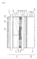
- Fig. 1 illustrates the structure of a typical OCB type liquid crystal display element.
- a backlight unit 103 which is a white light source, is disposed on the backside of a liquid crystal panel 113.
- the backlight unit comprises a light guide plate 101, a sidelight 102, and so forth.
- a liquid crystal (material) 114 having a predetermined thickness is held (or sandwiched when there are two substrates) between two substrates, upper and lower substrates (111 and 107).
- Color filters 112 for red, green, and blue are formed on the substrate 111, corresponding to each pixel.
- the other substrate is an active matrix substrate on which active elements, such as TFTs 108, are formed.
- black matrices 201 and 202 are formed between the color filters.
- the black matrix 202 facing the substrate is made of chromium oxide
- the black matrix 201 facing the liquid crystal is made of chromium metal.
- Transparent electrodes 109 made of ITO are formed on the front and back surfaces of the liquid crystal panel, serving as a means of applying voltage.
- OCB type liquid crystal display elements perform the display operation by applying a voltage so as to change the amount of birefringence and retardation (optical phase difference) of the liquid crystal layer. Therefore, in TN type liquid crystal elements as mentioned above, the rubbing directions that determine the direction of alignment of the liquid crystal differ by 90° between the upper and lower substrates so as to achieve a twisted alignment state, while in OCB type liquid crystal display elements, the parallel rubbing whereby liquid crystals on both upper and lower substrates are aligned in the same direction is employed.
- optical compensation films 106 and 105 are disposed on the outer surfaces of the upper and lower substrates.
- an optical compensation film 106 wherein a discotic liquid crystal is hybrid aligned, and an optical compensation film 105 that is biaxially stretched are used, for example.
- polarizing plates 104 are disposed on the outermost surfaces of the substrates. The polarizing axes of the polarizing plates are usually rotated by 45° with respect to the rubbing direction that determines the liquid crystal alignment. For example, when the upper polarizing plate is rotated by +45° and the lower polarizing axis is rotated by -45°, the axes of the upper and lower polarizing plates form an angle of 90°.
- OCB type liquid crystal display elements having such a structure as described above, first, a sufficient contrast (brightness in a bright display state / brightness in a dark display state) that meets the recent demand for improved display characteristics is difficult to obtain.
- the present invention has been accomplished as a result of the research carried out for solving the above-mentioned and other problems in prior art. Specifically, the present inventors have found and eliminated the factors that may inhibit the inventors from solving the problems in not only an OCB type element but a liquid crystal display element (including a liquid crystal switch and a liquid crystal logic element) comprising a liquid crystal having a mode of display such that graphics and results of computation are displayed by controlling the amount of birefringence, which liquid crystal in principle is sandwiched between two substrates, and thus have solved the foregoing problems. More specifically, the present invention has the following aspects.
- the reflected light that occurs in various parts of a liquid crystal display element is reduced.
- a liquid crystal display element having a liquid crystal (layer) wherein the display operation is performed by controlling the amount of birefringence the liquid crystal (layer) being in principle sandwiched between two substrates, or in a liquid crystal display element having a single substrate, in a special case, wherein a liquid crystal (layer) and an upper interfacial resin film are formed
- a light-blocking layer such as so-called black matrix and a light-blocking portion (non-light transmissive portion) for the perimeter of the display, is formed on at least one of the substrates.
- At least a portion of the light-blocking layer (preferable on the entire light-blocking layer, unless it is preferable that the light-blocking layer be formed on a portion thereof), at least the portion facing the liquid crystal layer, may be composed of a light absorbing material instead of such a material that simply provides a light blocking effect.
- the light from the backlight coming from the backside of the substrate reflects off the surface of the light-blocking layer on the upper substrate, which surface is on the side of the light-blocking layer facing the liquid crystal, toward the lower substrate, then reflects off the lower substrate back toward the upper substrate, and goes out of the display. Consequently, the reflected light is perceived by the user even in a dark display state, causing contrast reduction. This adverse effect is prevented by the above-described construction.
- a liquid crystal display element In a liquid crystal display element, at least one of the substrates, particularly a lower substrate that is away from the user, is an active matrix substrate having active elements made of a highly reflective material or white-colored such as polycrystalline silicon and highly reflective Wirings made of metal formed thereon. Therefore, a light absorbing material layer, a belt of films composed of a light absorbing material, or the like may be formed on at least a portion of the wirings and the active elements (preferably on the entire region over the wirings and the active elements, unless it is preferable that the light absorbing material layer or the like be formed on a portion thereof) and the like facing the liquid crystal, the wirings and the active elements being provided on at least one active matrix substrate (or on both substrates in principle if both substrates are active matrix substrates).
- the interfacial reflection that occurs at the boundary surfaces of the substrates, the transparent electrodes, the retardation films, and so forth is reduced.
- a transparent electrode is formed on at least one of the substrates, and an anti-reflection treatment may be carried out by forming a film, having an intermediate refractive index between that of the substrate and that of the transparent electrode, on the surface of the transparent electrode, or by forming an anti-reflection film on the surface of the transparent electrode.
- At least one retardation film in principle two retardation films provided on at least one substrate (in principle on both substrates) may be designed to have the surface reflectance of 1% or less. Also, the characteristics of the retardation film may be adjusted in various manners.
- a light absorbing material and a color filter are formed on an active matrix substrate having active elements and wirings formed thereon.
- the color filter material layer (film) is formed such that it extends over the active elements and the wirings that are formed outside the pixels, so that the extended portions can absorb the complementary colors of the color filter. Thereby, reflected light may be reduced without forming a light absorbing material layer composed of a resin matrix additionally.
- an anti-reflection film may be formed on an interface between the upper or lower substrate and the air.
- a light focusing means for focusing the light coming from the backlight in a front direction or in the direction directly toward a user may be provided, and/or a focused-light reflecting means for reflecting such a focused light may be provided.
- the light that is basically not supposed to be perceived by the user such as light traveling toward a non-light transmissive portion including the back surface of the black matrix on the substrate, the active elements, and the wirings on the active matrix substrate facing the liquid crystal, is minimized.
- the efficiency of utilizing light is improved, while preventing the reduction in the contrast caused by such light that reflects off the back surface of the black matrix and so forth and is perceived by the user eventually.
- the liquid crystal may be such a liquid crystal wherein the retardation value thereof is not zero during a black display state.
- the liquid crystal may be an OCB mode liquid crystal.
- Fig. 1 is a cross sectional view showing the structure of a conventional OCB type liquid crystal display element.
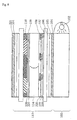
- Fig. 2 is a cross sectional view showing the structure of a liquid crystal display element of Example 1 according to the present invention.
- Fig. 3 is a schematic view for illustrating the causes of the contrast reduction in a conventional OCB type liquid crystal display element.
- Fig. 4 is a cross sectional view showing the structure of a liquid crystal display element of Example 2 according to the present invention.
- Fig. 5 is a cross sectional view showing the structure of a liquid crystal display element of Example 3 according to the present invention.
- Figs. 6(1) and 6(2) are cross sectional views showing the structures of a liquid crystal display element of Example 4 according to the present invention.
- Fig. 7 is a cross sectional view showing the structure of a liquid crystal display element of Example 5 according to the present invention.
- Fig. 8 is a cross sectional view showing the structure of a liquid crystal display element of Examples 6 and 8 according to the present invention.
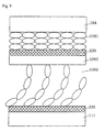
- Fig. 9 illustrates an adhesive layer and anti-reflection film for bonding two retardation films and for preventing interfacial reflection occurring between two retardation films in Example 7 according to the present invention.
- Fig. 10 is a cross sectional view showing the structure of a liquid crystal display element of Example 9 according to the present invention.
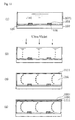
- Figs. 11(1) to 11(4) are cross sectional views showing the manufacturing process and the finished product of a liquid crystal display element of Example 10 according to the present invention.
- Fig. 12 is a diagram showing the structure of the system of a liquid crystal display element of Example 11 according to the present invention.
- Example 1 of the present invention relates to the prevention of reflection off the outer surface of a black matrix.
- Fig. 2 is a cross sectional view of the liquid crystal display element of Example 1 in accordance with the present invention.
- the liquid crystal display element includes the liquid crystal panel wherein a liquid crystal is sandwiched between two substrates, and the retardation films are formed on the outer surfaces of the liquid crystal panel. Further, the color filters are formed on one substrate, and the TFT elements, and so forth are formed on the other substrate, and also the backlight unit is disposed on the backside of the liquid crystal panel.
- the basic structure of the liquid crystal display element is the same as that of a conventional liquid crystal display element shown in Fig. 1, except that a black matrix 200, serving as a light-blocking layer, formed on the color filter substrate that is the upper substrate in Fig. 1 (the user's side), is composed of a resin BM (a black matrix made of resin).
- the resin BM is made of an acrylic resin containing a black pigment.
- a black matrix having a lattice structure in cases of so-called mosaic alignment is provided between pixels so as to obtain a clearer color for each pixel and to block the light that reaches the TFT silicone film.
- the present inventors have found that the light from the backlight reflects off the back surface of the black matrix (light-blocking layer), causing a great contrast reduction.
- a black matrix 601 is generally composed of layers of chromium oxide and chromium.
- a black chromium oxide 202 which is desirable in improving vividness of colors, is deposited on the inner surface (the surface facing the liquid crystal) of the upper substrate, and a chromium 201 having a metallic luster with an excellent light blocking effect is layered below the chromium oxide 202. Due to this structure, the surface of the black matrix contacting the liquid crystal layer has a metallic luster, and thus, it is inevitable that the light traveling from the inside in an upward direction reflects off the metallic-lustered portion toward the inside.
- the light entering the liquid crystal panel from the backlight passes through a lower polarizing plate 104, lower retardation films 105 and 106, followed by a liquid crystal layer only once, and further through upper retardation films 106 and 105 and an upper polarizing plate 104 so that the light can go out of the element.
- This is schematically illustrated by the arrow (1) in Fig. 3.
- a mode using birefringence such as an OCB type liquid crystal display element, when the light passes through the element, the total amount of retardation of the light is controlled.
- the retardation that occurs on the liquid crystal layer while the voltage for the black display state is being applied should be compensated with the retardation of the retardation films disposed on the outer surfaces of the upper and lower substrates.
- the upper and lower polarizing plates are under crossed Nicols, in which the plates are perpendicular to each other.
- the back surface of the black matrix 201 has a metallic luster, as shown in Figs. 1 and 3, light reflection occurs at the back surface. Moreover, light reflection occurs at the white-colored or metallic-lustered portions, such as the TFTs and the wirings, provided on the lower substrate shown in Figs. 1 and 3. A slight light reflection also occurs at the surface of an ITO transparent electrode.
- the project areas occupied by the black matrix, active elements, and wirings are quite large with respect to the display area, and the reflectances thereof are also large. These factors have been part of the causes of a reduction in the contrast of the display surface.
- the upper and lower retardation films have a retardation value of 30 nm and the liquid crystal layer has a retardation value of 60 nm.
- a retardation value of 120 nm remains even after the light has passed through the films. It turns out to serve as a ⁇ /4 plate, and the transmissivity of the component reaches as high as a brightness of 50% with respect to white, which is the greatest.
- the phenomenon or problem of a reduction in contrast caused by the reflected light occurs particularly in such a mode where a liquid crystal layer has birefringence in a black state, and the retardation value of the liquid crystal layer is not zero.
- the retardation value is zero, such problem will not occur even if light passes through the liquid crystal layer multiple times.
- the retardation of the films are controlled so as to compensate the retardation that occurs in the liquid crystal layer while the voltage for a black display state is being applied. In such elements, it is desirable to consider interfacial reflection.
- retardation films are attached to the front and back surfaces of the panel, and the retardation values of such retardation films in a front direction are not zero.
- the black matrix was formed by using the resin in which a black pigment is dispersed (the material for this black matrix is hereinafter referred to as "resin BM"), as shown in Fig. 2. Since the back surface of the resin BM as well as a front surface thereof is black, which differs from a conventional black matrix, little light reflection from the inside to the upward direction occurs. Therefore, reflected light almost never travels toward the user during a black display state in such a manner that the light from the backlight reflects off the back surface of the black matrix, and then, reflects off the front surface of the lower substrate again. Consequently, significant improvement in contrast is achieved.
- resin BM the material for this black matrix
- the liquid crystal display element of Example 1 achieved a contrast ratio of 200.
- the present invention differs from the prior art in that a two-step process is not required for forming a black matrix. As a result, there is no increase in cost, and also a situation wherein the upper and lower layers are not precisely aligned does not occur. These points also made the present invention preferable.
- the black matrix is not limited to the resin BM.
- a general chromium oxide-chromium layered structure may be employed instead.
- a triple-layer structure of chromium oxide/chromium/chromium oxide may be employed.
- a single-layer structure of chromium oxide may be employed, in case of which, it needs to form a thicker layer.
- the pigment used in the resin BM it is not limited to a black material but mixed materials with various colors may also be used as long as they provide the light absorption effect.
- the resin used for the resin BM other materials that do not adversely affect the liquid crystal and that are easy to form may be used.
- the black matrix in the display area has been discussed thus far. It is noted, however, that reflected light that affects the contrast of a liquid crystal display element is not limited to the light reflected by the black matrix. It is often the case that a black frame with a width of about 2 to 5 mm, serving as a light-blocking layer, is formed around the perimeter of the display area of a liquid crystal display element. Conventionally, the black frame was made of the same material used in the black matrix for the sake of convenience in manufacturing, and therefore, the back surface of the black frame also had a metallic luster. Thus, light leakage occurs around the black frame. By using a light absorbing material in the back surface of the black frame, it is possible to reduce the light leakage around the display area.
- the liquid crystal used in the present invention is not limited to a liquid crystal having a mode of an OCB type. More specifically, the invention can be applied to any types of liquid crystals or display elements comprising a liquid crystal as long as they have such a mode that the display operation is performed by using birefringence. For example, an ASV (Advanced Super V) mode that is rubbed in a parallel direction may also be used.
- ASV Advanced Super V
- the present invention since one of the problems to be solved relates to very small influence of the reflected light, the higher the contrast is, the more serious the problem becomes.
- the present invention is effective on a display element with a contrast ratio of 100 or higher, and has a distinctive effect on a display element with a contrast ratio of 200 or higher. Also, the present invention was effective on STN type display elements; however, the effect was not so great since such elements have basically low contrast.
- Example 2 of the present invention relates to anti-reflection measures employed on an array substrate.
- Example 1 of the present invention in order to prevent reflection from the upper substrate, a light absorbing material was used in the back surface of the black matrix.
- the ITO transparent electrode is formed on the upper substrate, which generates the difference in the refractive indices of the materials thereof, a slight reflection also occurs at the liquid crystal/ITO interface and at the ITO/substrate interface.
- the resin BM is used in the black matrix on the upper substrate, the reflection of light off of the upper substrate toward the lower substrate cannot be eliminated completely.
- the reflected light from the liquid crystal/ITO interface reflects off the lower substrate toward the upper substrate again, the reflected light will cause contrast reduction more or less due to the above-described reason.
- the lower substrate is an active matrix substrate on which a plurality of TFTs, metal wirings, and so forth are formed, occupying a fairly large area with respect to the display area, and therefore, for the reasons described above, the reflected light reflects off those components back toward the upper substrate.
- the area occupied by the wirings is larger than that occupied by the active elements.
- the light coming from the upper substrate reflects off the components toward the upper substrate.
- Example 2 the resin layers in which a light absorbing pigment was dispersed, that is "resin BM 301" as referred in the present invention, were formed over the top surfaces of the TFTs/wirings 108 provided on the lower substrate 107, as shown in Fig 4. Thereby, the light reflection off of the lower substrate in an upward direction was reduced, and contrast was improved, resulting in a contrast ratio of 250.
- the light absorbing material is not limited to the resin BM.
- Example 3 of the present invention only the ITO transparent electrode is formed on the upper substrate, and the array comprising TFTs, electrodes, and wirings and color filters are formed on the lower substrate.
- Fig. 5 schematically illustrates a principal portion of the liquid crystal display element of Example 3 in accordance with the present invention. As shown in the central part of Fig. 5, a green (G) color filter 112, serving as the resin BM, is formed on the lower substrate 107 such that the green color filter is a little bit bigger than pixel size. Therefore, this color filter has an extended portion 1121 over the array and over metal wiring 108 provided on the lower substrate.
- G green
- Example 3 first, only the transparent electrode 109 is formed on the upper substrate 111, which means the number of the member contributing to reflection is small, and accordingly a higher contrast than the contrast achieved by Example 2 was achieved. More specifically, a contrast ratio of 300 was obtained.
- Example 3 since the portions provided on the lower substrate are made of metal, reflection, especially from the wirings, causes a problem.
- the whole reflected light was not absorbed, just by forming a green color filter over the metal wiring, a practically sufficient effect is exhibited. That is, the color filter is capable of absorbing the reflected light of complementary color that affects the sensitivity of human eyes.
- Example 3 it is not necessary to form the resin BM additionally, providing the cost-cut effect.
- the resin BM capable of absorbing light completely may be formed over the top surfaces of the active elements and the wirings. It is also possible that color filters for other colors may be used for attaining part of the functions of the resin BM, depending on the pixel arrangement or the like.
- Example 4 of the present invention the attention is focused on the incident angle of reflected light, and thus, a light focusing means is employed.
- the previous Examples 1 to 3 discussed the reduction of the reflected light occurring at the back surface of the black matrix and at the array wirings.
- the black matrix provided on the opposing substrate and the array wirings provided on the array substrate are designed such that the black matrix and the array wirings are overlapped when viewed from the direction orthogonal to the substrate surface. Therefore, the light entering the back surface of the black matrix from the vertical direction and the light entering the array wirings from the vertical direction usually reflects off each other, and the light ends up attenuating. As a result, such light does not have much influence on the contrast reduction.
- the light entering the surface of the substrate from an oblique direction is the light that reflects internally and thereby adversely affects contrast.
- a light focusing means such as a prism sheet 210
- a liquid crystal panel 113 and a light guide plate 101 in order to direct the light from the backlight toward the direction orthogonal to the surface of the substrate, that is in a front direction, and to attenuate oblique light itself, it is possible to reduce contrast reduction caused by such reflection.
- the reference numeral 210 shows the prism sheet, and the function thereof is illustrated in Fig. 6(2).
- Example 5 of the present invention is similar to the previous Example 4.
- a focused-light reflecting means 211 for reflecting the light from the backlight in a front direction is provided on the back surface (the other side of the front side) of the light guide plate 101, as shown in Fig. 7.
- Example 4 The same effect as Example 4 was also provided by the present Example.
- Example 6 of the present invention describes the prevention of reflection that occurs between layers having different refractive indices.
- the ITO used in a transparent electrode has a refractive index of about 1.9 to 2.0, while the substrates and the liquid crystal layer contacting the ITO transparent electrode each have a refractive index of about 1.5.
- Fig. 8 schematically illustrates a principal portion of the liquid crystal display element of Example 6 in accordance with the present invention.
- anti-reflecting layers 220 which also serves as planarizing layers for reducing projections and depressions on the array substrate, are included on the ITO layer/liquid crystal interfaces, on the ITO layer/upper substrate interface, and on the ITO layer/lower substrate interface, by applying and curing acrylic resin layers having a refractive index of 1.7 that is an intermediate refractive index between that of the interfaces.
- the reflectance of the ITO surfaces was decreased, which provided a further improvement in contrast, achieving a contrast ratio of 400.
- the total intensity of the reflected light, when incident light is 100%, is 0.016%.
- reflection off of the TFTs and the wirings and of the back surface of the BM should also be added. Therefore, in conventional OCB panels, the intensity of reflected light reached as high as 0.05%.
- both front and back surfaces of the ITO transparent electrode were subjected to an anti-reflection treatment.
- an anti-reflection treatment needless to say, even when either the front surface or the back surface is subjected to such a treatment, a certain degree of effect can be provided.
- An organic conductive film with a refractive index of about 1.7 may also be used instead of an acrylic resin. Thereby, the effect of decreasing electric resistance can be provided on the ITO film additionally.
- Example 7 of the present invention relates to measures to prevent interfacial reflection that occurs within the retardation films.
- the retardation film has a two-layered structure, light reflection even occurs at the interface between the layers.
- a film wherein a discotic liquid crystal is hybrid aligned since such film is formed on a base film having a refractive index of 1.5, the alignments of the liquid crystal molecules of the film and that of the base film differ from each other, causing a difference in the refractive indices between the top and bottom films.
- a surface of a parallel-aligned discotic liquid crystal had a refractive index of about 1.7 to 2.0, and there was a high rate of occurrence of light reflection at the interfaces between the surface and the base film, and between the surface and the glass.
- a bonding layer having a refractive index of 1.6 between each of the interfaces or by including an adhesive layer having a refractive index of 1.6 between each of the interfaces, so as to bond the two films together, interfacial reflection has been reduced, which is illustrated in Fig. 9.
- the reference numeral 104 indicates a polarizing plate.
- the reference numeral 1061 indicates a film in which discotic liquid crystal having a refractive index of 1.7 is parallel aligned.
- the reference numeral 230 indicates an adhesive layer having a refractive index of 1.6.
- the reference numeral 1062 indicates a base film having a refractive index of 1.5.
- the reference numeral 1063 indicates a film in which discotic liquid crystal having a refractive index of 1.6 is hybrid aligned.
- the reference numeral 111 indicates an upper glass substrate.
- Example 8 of the present invention relates to liquid crystal display elements in which an interface between the air and the polarizing plate, which is the outermost portion of the liquid crystal display element, is subjected to an anti-reflection treatment.
- an interface between the air and the polarizing plate which is the outermost portion of the liquid crystal display element
- light reflects off the outer surface of the polarizing plate when the polarizing plate is not subjected to an anti-reflection treatment.
- Such a problem is less likely to occur in the case of the light coming from a vertical direction.
- reflection cannot be eliminated completely since the crossing angle in the polarizing plates for the light coming from oblique directions differs from that for the light coming from the front directions.
- internally reflected lights having different retardations are generated. Since such internally reflected light causes a bluish color shift, when the element in a black display state is viewed from oblique directions, the bluish color shift appears in the displayed image.
- a surface of a polarizing plate is subjected to an anti-reflection treatment, and thereby the internally reflected light resulting from the oblique light is reduced.
- Fig. 7 shows such an anti-reflection film 221.
- Example 9 of the present invention relates to light-reflective type liquid crystal display elements.
- Fig. 10 shows a cross sectional view of the liquid crystal display element of Example 9 in accordance with the present invention.
- the reference numeral 1091 shows a lower electrode film of the light-reflective type liquid crystal display element.
- the liquid crystal of the element is hybrid aligned wherein one side is parallel aligned and the other side is vertically aligned. This structure is generally called ROCB.
- Example 9 all the black matrices on the upper substrate are the resin BM 200 composed of a light absorbing material.
- the upper substrate can be an array substrate.
- Example 10 of the present invention relates to the case where only one substrate is used.
- a substrate having TFTs and wirings thereon, which are formed in advance, is prepared, and a layer of a mixture containing a material for forming a liquid crystal and a material for forming a transparent resin film is formed thereover.
- a liquid crystal layer is formed in the lower portion and a transparent resin film, which functions as an upper substrate, is formed in the upper portion. This is shown in Figs. 11(1) to 11(3). In Fig.
- the reference numeral 107 indicates a lower substrate
- the reference numeral 109 indicates a lower transparent electrode for pixels formed on top of the lower substrate
- the reference numeral 108 indicates an array of active elements, wirings, and so forth.
- the reference numeral 301 indicates a light absorbing material film having a substantially lattice structure.
- the reference numeral 1071 indicates a sidewall portion.
- the reference numeral 1141 indicates a mixture containing a liquid crystal material and a transparent resin film material.
- a liquid crystal layer 114 is formed on a lower substrate side, and a transparent resin film 1111 is formed on top thereof.
- Fig. 11(4) shows a state of the finished product
- the reference numeral 1091 indicates an upper transparent electrode made of an organic conductive resin
- the reference numeral 2201 indicates an anti-reflection film and insulated film made of a transparent resin having a refractive index of about 1.3 that is an intermediate refractive index between that of the air and that of the organic conductive resin film.
- the present example relates to liquid crystal logic elements.
- optical logic elements as shown in Fig. 12 have been developed.
- the optical logic element 42 receives an incident light 40, and outputs the results of computation as a passing light 41.
- Such an element requires a high contrast ratio when applied to optical computers.
- a high contrast ratio is achieved.
- One of the objects of the present invention is to provide liquid crystal display elements with OCB or other types having an exceptional contrast ratio and so forth by reducing various types of interfacial reflections or the like. Therefore, combinations of any of Examples 1 to 11 may be employed so as to reduce reflected light.
- liquid crystal display element with excellent display characteristics, such as high contrast, particularly when an OCB mode liquid crystal is used therein.
Landscapes
- Physics & Mathematics (AREA)
- Nonlinear Science (AREA)
- Chemical & Material Sciences (AREA)
- Crystallography & Structural Chemistry (AREA)
- General Physics & Mathematics (AREA)
- Optics & Photonics (AREA)
- Mathematical Physics (AREA)
- Engineering & Computer Science (AREA)
- Microelectronics & Electronic Packaging (AREA)
- Liquid Crystal (AREA)
Applications Claiming Priority (5)
| Application Number | Priority Date | Filing Date | Title |
|---|---|---|---|
| JP21469499 | 1999-07-29 | ||
| JP21469499 | 1999-07-29 | ||
| JP29968299 | 1999-10-21 | ||
| JP29968299 | 1999-10-21 | ||
| PCT/JP2000/005000 WO2001009673A1 (en) | 1999-07-29 | 2000-07-26 | Liquid crystal display device |
Publications (2)
| Publication Number | Publication Date |
|---|---|
| EP1118902A1 true EP1118902A1 (de) | 2001-07-25 |
| EP1118902A4 EP1118902A4 (de) | 2004-03-17 |
Family
ID=26520458
Family Applications (1)
| Application Number | Title | Priority Date | Filing Date |
|---|---|---|---|
| EP00949917A Withdrawn EP1118902A4 (de) | 1999-07-29 | 2000-07-26 | Flüssigkristallanzeigevorrichtung |
Country Status (5)
| Country | Link |
|---|---|
| EP (1) | EP1118902A4 (de) |
| KR (1) | KR20010072446A (de) |
| CN (1) | CN1316064A (de) |
| TW (1) | TW538268B (de) |
| WO (1) | WO2001009673A1 (de) |
Cited By (3)
| Publication number | Priority date | Publication date | Assignee | Title |
|---|---|---|---|---|
| EP1245995A3 (de) * | 2001-03-30 | 2004-12-15 | Matsushita Electric Industrial Co., Ltd. | Flüssigkristallanzeige |
| WO2014004387A1 (en) * | 2012-06-29 | 2014-01-03 | Qualcomm Mems Technologies, Inc. | Illumination systems incorporating a light guide and a reflective structure and related methods |
| US20230054796A1 (en) * | 2021-08-19 | 2023-02-23 | Interface Technology(Chengdu) Co., Ltd. | Optical display structure |
Families Citing this family (12)
| Publication number | Priority date | Publication date | Assignee | Title |
|---|---|---|---|---|
| KR100925452B1 (ko) | 2002-08-14 | 2009-11-06 | 삼성전자주식회사 | Ocb 모드 액정 표시 장치 그 구동 방법 |
| KR100483659B1 (ko) * | 2002-08-23 | 2005-04-19 | 에이유 오프트로닉스 코퍼레이션 | Tft-lcd의 백라이트 유닛 |
| CN100464213C (zh) * | 2005-05-28 | 2009-02-25 | 群康科技(深圳)有限公司 | 穿透式液晶显示装置 |
| TWI600958B (zh) | 2012-03-09 | 2017-10-01 | 元太科技工業股份有限公司 | 電泳顯示面板及其製作方法 |
| CN102879948B (zh) * | 2012-09-29 | 2015-10-21 | 京东方科技集团股份有限公司 | 彩膜基板、液晶显示装置及制作方法 |
| KR102112520B1 (ko) * | 2013-03-07 | 2020-05-19 | 도레이 카부시키가이샤 | 블랙 매트릭스 기판 |
| JP2018112616A (ja) * | 2017-01-10 | 2018-07-19 | 富士フイルム株式会社 | 積層体、積層体の製造方法、および車両用ルームミラー |
| CN106772777B (zh) * | 2017-02-20 | 2019-07-26 | 京东方科技集团股份有限公司 | 一种显示装置和显示装置的制备方法 |
| CN106990596A (zh) * | 2017-05-12 | 2017-07-28 | 武汉华星光电技术有限公司 | 彩膜基板和液晶显示器 |
| JP2019029057A (ja) * | 2017-07-25 | 2019-02-21 | 株式会社小糸製作所 | 光源モジュール及び車両用灯具 |
| CN107728417B (zh) * | 2017-11-10 | 2020-06-05 | 广州西岛电子科技有限公司 | 液晶投影屏幕 |
| CN111208675B (zh) * | 2020-03-06 | 2022-06-21 | 京东方科技集团股份有限公司 | 显示面板和显示装置 |
Family Cites Families (13)
| Publication number | Priority date | Publication date | Assignee | Title |
|---|---|---|---|---|
| DE3137518C2 (de) * | 1981-09-21 | 1985-11-07 | Siemens AG, 1000 Berlin und 8000 München | Reflexionsarme Flüssigkristallanzeige |
| JPH06331973A (ja) * | 1993-05-26 | 1994-12-02 | Sharp Corp | 液晶表示装置 |
| JP3307181B2 (ja) * | 1995-07-31 | 2002-07-24 | ソニー株式会社 | 透過型表示装置 |
| JPH0996790A (ja) * | 1995-09-29 | 1997-04-08 | Toshiba Corp | 液晶電気光学素子 |
| JPH09146108A (ja) * | 1995-11-17 | 1997-06-06 | Semiconductor Energy Lab Co Ltd | 液晶表示装置およびその駆動方法 |
| JP3688036B2 (ja) * | 1995-12-04 | 2005-08-24 | 大日本印刷株式会社 | 非光拡散性導光板を用いた面光源装置、及びレンズフィルム |
| JPH10186379A (ja) * | 1996-12-25 | 1998-07-14 | Casio Comput Co Ltd | 液晶表示装置 |
| JP3658904B2 (ja) * | 1996-12-25 | 2005-06-15 | カシオ計算機株式会社 | 液晶表示装置 |
| US6038006A (en) * | 1996-09-02 | 2000-03-14 | Casio Computer Co., Ltd. | Liquid crystal display device with light shield and color filter overlapping two edges of pixel electrode |
| JP3949759B2 (ja) * | 1996-10-29 | 2007-07-25 | 東芝電子エンジニアリング株式会社 | カラーフィルタ基板および液晶表示素子 |
| JP4004599B2 (ja) * | 1997-09-26 | 2007-11-07 | 日本ライツ株式会社 | 導光板および平面照明装置 |
| JPH11149015A (ja) * | 1997-11-14 | 1999-06-02 | Nitto Denko Corp | 積層波長板、円偏光板及び液晶表示装置 |
| JPH11160703A (ja) * | 1997-11-21 | 1999-06-18 | Sony Corp | 表示装置 |
-
2000
- 2000-07-26 WO PCT/JP2000/005000 patent/WO2001009673A1/ja not_active Ceased
- 2000-07-26 KR KR1020017001853A patent/KR20010072446A/ko not_active Withdrawn
- 2000-07-26 EP EP00949917A patent/EP1118902A4/de not_active Withdrawn
- 2000-07-26 CN CN00801220A patent/CN1316064A/zh active Pending
- 2000-07-28 TW TW089115129A patent/TW538268B/zh not_active IP Right Cessation
Cited By (5)
| Publication number | Priority date | Publication date | Assignee | Title |
|---|---|---|---|---|
| EP1245995A3 (de) * | 2001-03-30 | 2004-12-15 | Matsushita Electric Industrial Co., Ltd. | Flüssigkristallanzeige |
| WO2014004387A1 (en) * | 2012-06-29 | 2014-01-03 | Qualcomm Mems Technologies, Inc. | Illumination systems incorporating a light guide and a reflective structure and related methods |
| US8872764B2 (en) | 2012-06-29 | 2014-10-28 | Qualcomm Mems Technologies, Inc. | Illumination systems incorporating a light guide and a reflective structure and related methods |
| US20230054796A1 (en) * | 2021-08-19 | 2023-02-23 | Interface Technology(Chengdu) Co., Ltd. | Optical display structure |
| US12027650B2 (en) * | 2021-08-19 | 2024-07-02 | Interface Technology (Chengdu) Co., Ltd. | Optical display structure |
Also Published As
| Publication number | Publication date |
|---|---|
| EP1118902A4 (de) | 2004-03-17 |
| WO2001009673A1 (en) | 2001-02-08 |
| TW538268B (en) | 2003-06-21 |
| KR20010072446A (ko) | 2001-07-31 |
| CN1316064A (zh) | 2001-10-03 |
Similar Documents
| Publication | Publication Date | Title |
|---|---|---|
| US6341002B1 (en) | Liquid crystal display device | |
| US6690438B2 (en) | Liquid crystal display panel | |
| US5847789A (en) | Reflective type liquid crystal display device | |
| EP1118902A1 (de) | Flüssigkristallanzeigevorrichtung | |
| US7310125B2 (en) | Reflective liquid crystal display | |
| JP2004109629A (ja) | 液晶表示装置 | |
| JP3806104B2 (ja) | 半透過型液晶表示装置及びその製造方法 | |
| US6933994B1 (en) | Liquid crystal display including an anisotropic scattering layer | |
| US6072553A (en) | Reflection-type liquid crystal display with layer comprising liquid crystal compound and liquid crystal polymer being twist-aligned at same angle | |
| KR100915235B1 (ko) | 반투과형 액정 표시 장치 | |
| JP2000066195A (ja) | 反射型液晶表示素子 | |
| KR101415573B1 (ko) | 액정표시장치 | |
| EP0982623B1 (de) | Reflektierende Flüssigkristall-Anzeigevorrichtung | |
| JP2892913B2 (ja) | 反射型液晶表示装置 | |
| US20060164574A1 (en) | Liquid crystal display | |
| JP2003131268A (ja) | 液晶表示装置 | |
| US20050140901A1 (en) | Fringe field switching liquid crystal display | |
| JPH1152351A (ja) | 液晶表示装置 | |
| JP2000056125A (ja) | 液晶表示装置 | |
| JP2003207634A (ja) | 光学素子および液晶表示装置 | |
| JP2001188226A (ja) | 液晶表示素子 | |
| JP3575608B2 (ja) | 液晶表示装置 | |
| JP2002116439A (ja) | 液晶表示素子 | |
| US6163667A (en) | Semi-transmissive liquid crystal display device free from reversal of display on screen | |
| JP2000029021A (ja) | 反射型液晶表示装置 |
Legal Events
| Date | Code | Title | Description |
|---|---|---|---|
| PUAI | Public reference made under article 153(3) epc to a published international application that has entered the european phase |
Free format text: ORIGINAL CODE: 0009012 |
|
| 17P | Request for examination filed |
Effective date: 20010420 |
|
| AK | Designated contracting states |
Kind code of ref document: A1 Designated state(s): AT BE CH CY DE DK ES FI FR GB GR IE IT LI LU MC NL PT SE |
|
| AX | Request for extension of the european patent |
Free format text: AL;LT;LV;MK;RO;SI |
|
| A4 | Supplementary search report drawn up and despatched |
Effective date: 20040203 |
|
| RIC1 | Information provided on ipc code assigned before grant |
Ipc: 7G 02F 1/1362 B Ipc: 7G 02F 1/139 A Ipc: 7G 02F 1/1335 B |
|
| RBV | Designated contracting states (corrected) |
Designated state(s): DE FR GB |
|
| STAA | Information on the status of an ep patent application or granted ep patent |
Free format text: STATUS: THE APPLICATION HAS BEEN WITHDRAWN |
|
| 18W | Application withdrawn |
Effective date: 20040611 |