EP1116324B1 - Differential amplifier with gain linearization through transconductance compensation - Google Patents
Differential amplifier with gain linearization through transconductance compensation Download PDFInfo
- Publication number
- EP1116324B1 EP1116324B1 EP99946680A EP99946680A EP1116324B1 EP 1116324 B1 EP1116324 B1 EP 1116324B1 EP 99946680 A EP99946680 A EP 99946680A EP 99946680 A EP99946680 A EP 99946680A EP 1116324 B1 EP1116324 B1 EP 1116324B1
- Authority
- EP
- European Patent Office
- Prior art keywords
- transistors
- differential amplifier
- differential
- transistor
- coupled
- Prior art date
- Legal status (The legal status is an assumption and is not a legal conclusion. Google has not performed a legal analysis and makes no representation as to the accuracy of the status listed.)
- Expired - Lifetime
Links
- 238000000034 method Methods 0.000 claims description 7
- 230000001419 dependent effect Effects 0.000 claims description 2
- 230000003247 decreasing effect Effects 0.000 description 2
- 239000000654 additive Substances 0.000 description 1
- 230000000996 additive effect Effects 0.000 description 1
- 239000003990 capacitor Substances 0.000 description 1
- 238000006880 cross-coupling reaction Methods 0.000 description 1
- 230000003071 parasitic effect Effects 0.000 description 1
- 238000011084 recovery Methods 0.000 description 1
- 230000008054 signal transmission Effects 0.000 description 1
Images


Classifications
-
- H—ELECTRICITY
- H03—ELECTRONIC CIRCUITRY
- H03F—AMPLIFIERS
- H03F1/00—Details of amplifiers with only discharge tubes, only semiconductor devices or only unspecified devices as amplifying elements
- H03F1/32—Modifications of amplifiers to reduce non-linear distortion
- H03F1/3211—Modifications of amplifiers to reduce non-linear distortion in differential amplifiers
Definitions
- the present claimed invention relates to the field of differential amplifiers. More particularly, the present claimed invention relates to differential amplifiers that generate linear gain through transconductance compensation.
- Differential amplifiers are widely used in analog and digital circuits to amplify a differential voltage between two input signals. Ideally, a differential amplifier amplifies only the difference between the input signals while rejecting common-mode input changes such as noise. Differential amplifiers have found important applications where signals are contaminated by noise signals. For example, digital signals transmitted over a long cable may pick up miscellaneous noise signals during the signal transmission. The differential amplifiers reject the noise signals while amplifying the digital signals, thereby leading to the recovery of the original signals.
- the gain of conventional differential amplifiers may vary in response to a change in temperature. This is because base-emitter voltages of individual transistors in the differential amplifiers are highly sensitive to temperature variation. Since base-emitter voltages affect the transconductance of a transistor, the gain of the differential amplifier may not be constant or linear when such temperature variation occurs. In such cases, the gain of the conventional differential amplifiers may not be predictable due to the temperature variations.
- the conventional differential amplifiers may not provide sufficient gain for today's state of the art low current or low voltage applications.
- the state of the art high speed analog or digital circuits often employ low currents and/or low voltages to speed up the operation of the circuit while reducing power requirements for continuously decreasing die sizes.
- the conventional differential amplifiers may not provide a large enough gain to operate properly in high speed applications.
- EP 0648010 discloses a differential amplifier having a Darlington differential pair and a cross-coupled transistor pair to increase the transconductance of the Darlington differential pair.
- a capacitor connected between the bases of the cross-coupled transistor pair and a pair of resisters enables compensation at high frequencies for negative input impedance of the differential amplifier and reduces the gain of the differential amplifier.
- a transconductance compensating circuit for a differential amplifier having a main differential pair comprising: input means for receiving and shifting an input differential voltage signal to develop a shifted differential voltage signal; and first differential current means for providing a first differential current inversely to the input means to compensate for a change in a transconductance of the input means; characterised by a first resistor and a second resistor coupled directly to each other in use at a junction in series between the main differential pair.
- a differential amplifier comprising a circuit as defined above; and a main differential amplifier, including said first resistor and said second resistor coupled in series, coupled to receive the shifted differential voltage signal and being configured to amplify the shifted differential voltage signal to generate an output voltage signal.
- the present invention fills these needs by providing a differential amplifier having transconductance compensating circuitry to provide a linear gain over a wide input range. It should be appreciated that the present invention can be implemented in numerous ways, including as a process, an apparatus, a system, a device, or a method. Several inventive embodiments of the present invention are described below.
- the present invention provides a differential amplifier including an emitter follower pair, a first differential pair, and a main differential amplifier.
- the emitter follower pair is operative to receive an input differential voltage signal for shifting the input differential voltage signal to develop a shifted differential voltage signal.
- the first differential pair is configured to feed a first differential current inversely to the emitter follower pair so that a transconductance of the emitter follower pair changes inversely to compensate for a change in a transconductance of the first differential pair.
- the main differential amplifier is coupled to receive the shifted differential voltage signal and is configured to amplify the shifted differential voltage signal to generate an output voltage signal.
- the present invention provides a transconductance compensating circuit for a differential amplifier having a main differential pair.
- the compensating circuit includes an emitter follower pair and a first differential pair.
- the emitter follower pair is operative to receive an input differential voltage signal for shifting the input differential voltage signal to develop a shifted differential voltage signal.
- the first differential pair is configured to feed a first differential current inversely to the emitter follower pair such that a transconductance of the emitter follower pair changes inversely to compensate for a change in a transconductance of the first differential pair.
- the present invention provides a method for compensating variations in transconductance of a differential amplifier.
- the method includes (a) receiving, by a pair of emitter follower transistors, a differential input voltage; (b) providing, by a pair of differential pair of transistors, a compensating differential current inversely to the emitter follower transistors; (c) changing a transconductance of the emitter follower transistors inversely to compensate for a change in a transconductance of the differential pair transistors; and (d) shifting, by the emitter follower pair of transistors, the DC voltage level of the differential input voltage by a specified voltage in accordance with the change in the transconductance of the emitter follower pair transistors.
- a transconductance compensating circuit for a differential amplifier includes input means and differential current providing means.
- the input means receives and shifts an input differential voltage signal to develop a shifted differential voltage signal.
- the differential current providing means provides a first differential current inversely to the input means such that a transconductance of the receiving and shifting means changes inversely to compensate for a change in a transconductance of the differential current providing means.
- the differential amplifier of the present invention provides a large linear gain over a wide input range by compensating for transconductance variations of differential amplifier transistors.
- the differential amplifier provides such linear gain even in low current and low voltage applications by utilizing level shifting circuitry.
- the gain of the differential amplifier is highly predictable because the gain depends only on a set of resistors and not on the transconductance of transistors in the differential amplifier.
- differential amplifier having transconductance compensating circuitry to provide a linear gain over a wide input range
- numerous specific details are set forth in order to provide a thorough understanding of the present invention.
- the present invention may be practiced without these-specific details.
- well known methods, procedures, components, and circuits have not been described in detail so as not to unnecessarily obscure aspects of the present invention.
- the differential amplifier of the present invention provides a large and predictable linear gain over a wide input voltage range.
- the differential amplifier provides a main differential pair and a secondary differential pair coupled in parallel with the main differential pair.
- the main differential pair develops a first differential current and the secondary differential pair develops a second differential current.
- the first differential current is applied to a pair of load resistors to generate a differential output voltage.
- the second differential current is applied inversely to an emitter follower pair.
- the inversely applied second differential current operates to produce a base-emitter voltage drop in emitter follower pair that substantially compensates for a change in a base-emitter voltage drop in the main and secondary differential pairs.
- the value of load resistance and emitter series feedback resistance in the differential amplifier determines the amount of linear gain.
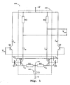
- a differential amplifier 100 includes a main differential amplifier 102, a secondary differential pair, and an emitter follower pair in accordance with one embodiment of the present invention.
- the main differential amplifier 102 includes a main differential pair, a pair of load resistors R3 and R4, a pair of emitter series feedback resistors R1 and R2, and a current source 106.
- the main differential pair includes a pair of transistors Q5 and Q6.
- Transistors Q5 and Q6 are preferably bipolar junction transistors, each having a base, a collector, and an emitter.
- the collectors of transistors Q5 and Q6 are coupled to resistors R3 and R4, respectively, which are, in turn, coupled to a positive supply voltage potential, +V.
- the emitters of transistors Q5 and Q6 are coupled to the emitter series feedback resistors R1 and R2, respectively.
- the emitter series feedback resistors R1 and R2 are coupled to each other at a junction 104.
- the current source 106 is coupled between the junction 104 of resistors R1 and R2 and a negative supply voltage potential, -V.
- the current source provides constant currents I R1 and I R2 through resistors R1 and R2, respectively.
- the main differential amplifier is configured to be symmetrical.
- transistors Q5 and Q6 are matching transistors having substantially equal emitter areas.
- the load resistors R3 and R4 are matching resistors.
- the emitter series feedback resistors R1 and R2 are also matching resistors.
- the symmetry of the main differential amplifier causes the current I1 of the current source 106 to be split evenly between the two transistors Q5 and Q6. That is, the currents I R1 and I R2 are approximately equal and each current has a value of about 1/2 of the current I1 provided by the current source 106. Further, if the base currents of the transistors Q5 and Q6 are assumed to be approximately zero, the collector currents I C5 and I C6 of transistors Q5 and Q6, respectively, are approximately equal to the currents I R1 and I R2 , respectively. Since the currents I R1 and I R2 are approximately equal, the collector currents of transistors Q5 and Q6 are also approximately equal.
- the collector currents I C5 and I C6 causes a differential voltage drop across the load resistors R3 and R4, respectively, to generate an output differential voltage signal Vout.
- the present invention employs a differential output voltage, those skilled in the art will appreciate that it may also take an output voltage from either collector of transistors Q5 and Q6.
- the secondary differential pair includes a pair of transistors Q3 and Q4, which are preferably bipolar junction transistors having a base, an emitter, and a collector.
- Transistors Q3 and Q4 are coupled in parallel to the transistors Q4 and Q6, respectively, and are arranged in a symmetrical configuration in the differential amplifier 100.
- the base of transistor Q3 is coupled to the base of transistor Q5 to form common-base transistors Q3 and Q5 while the base of transistor Q4 is coupled to the base of transistor Q6 to form common-base transistors Q4 and Q6.
- the transistors Q3 and Q4 are preferably matching transistors having matching emitter areas.
- the collectors of transistors Q3 and Q4 are cross-coupled in the differential amplifier 100.
- the collector of transistor Q3 is coupled to the common bases of transistors Q4 and Q6 whereas the collector of transistor Q4 is coupled to the common bases of transistors Q3 and Q5.
- the emitter follower pair is coupled to the common bases to form a compensation circuit and includes a pair of transistors Q1 and Q2 configured to receive a differential input voltage signal, Vin.
- Transistors Q1 and Q2 are preferably bipolar junction transistors having an emitter, a collector, and a base. The collectors of transistors Q1 and Q2 are coupled to a positive supply voltage potential, +V.
- the emitter of the emitter follower transistor Q1 is coupled to the common base of transistors Q3 and Q5 while the emitter of the emitter follower transistor Q2 is coupled to the common base of transistors Q4 and Q6.
- Transistors Q1 and Q2 receive the differential input voltage signal, Vin, across the base terminals.
- the differential output voltage signal, Vout is taken across the collectors of the main differential transistor pair Q5 and Q6.
- transistors Q1 and Q2 are matching transistors.
- the matching transistors Q1 and Q2 are also matched to matching transistors Q3 and Q4 in accordance with a preferred embodiment of the present invention.
- all four transistors Q1, Q2, Q3, and Q4 are matching transistors with substantially identical emitter areas A1, A2, A3, and A4, respectively.
- the base currents of all transistors in the differential amplifier 100 are assumed to be negligible.
- the emitter and collector currents of the each of the transistors in the differential amplifier 100 are assumed to be equal.
- the emitter areas of the transistors determine the division of current I1 in the differential amplifier 100.
- the current I1 which is provided by the current source 106, is split evenly between currents I R1 and I R2 through resistors R1 and R2, respectively, due to symmetry of the differential amplifier 100.
- Current I R1 is the sum of currents I C3 and I C5 while current I R2 is the sum of currents I C4 and I C6 .
- transistors Q4 and Q6 are matching transistors having substantially equal emitter areas. Similarly transistors Q3 and Q5 are also matching transistors having substantially same emitter areas. In a preferred embodiment, transistors Q1, Q2, Q3, Q4, Q5, and Q6 are matching transistors having matching emitter areas. In this matching transistor configuration, currents I R1 and I R2 are divided equally. That is, currents I C3 and I C5 are equal and currents I C4 and I C6 are equal. On the other hand, if the emitter area A6 of transistor Q6 is twice the area of Q4, for example, then one third of current I R2 flows through transistor Q4 and the rest flows through transistor Q6.
- the differential amplifier 100 provides two differential currents: a main differential current defined as a difference between currents I C5 and I C6 (e.g., I C5 -I C6 ) and a secondary differential current defined as a difference between currents I C3 and I C4 (e.g., I C3 -I C4 ).
- Currents I C5 and I C6 of the main differential current flow through the load resistors R3 and R4, respectively, to develop the differential output voltage Vout.
- the emitters of the emitter follower transistors Q1 and Q2 are cross-connected to the collectors of transistors Q4 and Q3, respectively.
- the cross-coupling of the transistors allows transistors Q3 and Q4 to feed currents I C3 and I C4 of the secondary differential current back to the emitter follower transistors Q2 and Q1, respectively.
- the differential amplifier 100 provides the secondary differential current inversely to the emitter follower transistors Q1 and Q2.
- the emitter follower transistors Q1 and Q2 are adapted to function as linearization circuitry by compensating for non-linear characteristics of transistors Q3 and Q4 so that transistors Q5 and Q6 may function in a linear mode.
- the emitter follower transistors Q1 and Q2 shift the DC voltage level of the differential input voltage Vin and feed the shifted input voltage to the bases of the main differential pair (e.g., transistor Q5 and Q6) and the secondary differential pair (e.g., transistors Q3 and Q4). Since the base-emitter voltage of a transistor is typically determined by its emitter area and emitter current, the differential amplifier 100 provides matching current to matching transistors in accordance with one embodiment of the present invention.
- transistors Q1, Q2, Q3, and Q4 are matching transistors with substantially identical emitter areas A1, A2, A3, and A4, respectively.
- the matching transistors Q3 and Q4, in particular, develop identical collector currents I C3 and I C4 .
- the matching transistors Q1 and Q4 have substantially identical current, I C3 , assuming negligible base currents.
- the feedback of the collector current I C4 as emitter current of transistor Q2 produces substantially identical base-emitter voltages V BE2 and V BE3 . Accordingly, the emitter follower transistors Q1 and Q2 compensates for variations in base-emitter voltages of transistors Q3 and Q4 to reduce non-linear characteristics of the differential amplifier 100.
- this compensation scheme also forces the base-emitter voltages V BE5 and V BE6 of transistors Q5 and Q6 to be equal to V BE3 and V BE4 , respectively. Moreover, if transistors Q5 and Q6 are matching transistors to Q3 and Q4, then the gain of transistors Q5 and Q6 will be substantially linear.
- the gain of the differential amplifier can be controlled by using resistor and transistors with appropriate resistance and emitter areas. For example, the gain can be decreased by means of the factor given in the above equation depending on the emitter areas of the transistors A3, A4, A5, and A6.
- the differential amplifier 100 may also be modified to provide a larger gain.
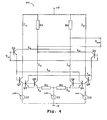
- Figure 2 illustrates a differential amplifier 200 in which the collector currents of emitter follower transistors Q1 and Q2 are fed back to the load resistors R4 and R3, respectively in accordance with one embodiment of the present invention.
- the feedback of the collector currents I C1 and I C2 to the load resistors R4 and R3, respectively, provides transconductance compensation by allowing additive superposition of the currents with the differential current from transistors Q5 and Q6. Accordingly, the differential amplifier 200 avoids loss of gain through this transconductance compensation.
- the differential amplifier 100 may also include an additional emitter follower pair to provide additional level shifting.
- Figure 3 illustrates a differential amplifier 300 having an additional level shifting between the emitter follower pair and the differential pairs in accordance with one embodiment of the present invention.
- the differential amplifier 300 adds an additional emitter follower pair between the common bases of the main and secondary differential pairs and the emitter follower pair of transistors Q1 and Q2.
- the additional emitter follower pair includes transistors Q7 and Q8, which are preferably bipolar junction transistors having a base, a collector, and an emitter.
- the bases of transistors Q7 and Q8 are coupled to the emitter of transistors Q1 and Q2.
- the collector of transistors Q7 and Q8 are coupled to positive voltage rail +V.
- the emitter of transistor Q7 is coupled to the common bases of transistors Q3 and Q5 while the emitter of transistor Q8 is coupled to the common bases of transistors Q4 and Q6.
- the transistors Q7 and Q8 are preferably matching transistors with substantially matching emitter areas.
- the differential amplifier 300 also provides a pair of current sources 108 and 110, which are coupled between the emitters of transistors Q7 and Q8, respectively, and negative voltage rail -V.
- the current sources 108 and 110 provide emitter currents 12 and 13, respectively, to transistors Q7 and Q8, respectively, for setting a proper operating point. Assuming that the base currents of transistors are negligible, the emitter currents I2 and I3 are equal to collector currents I C7 and I C8 of transistors Q7 and Q8, respectively.
- the additional emitter follower pair transistors Q7 and Q8 are provide additional level shifting of the differential input voltage Vin.
- the additional level shifting provides a voltage drop between the base and collector of transistors Q3 and Q4, thus allowing a larger amplitude for the output voltage Vout.
- the additional emitter follower provides additional current gain, which reduces the differential pair transistors' influence on the base currents.
- the gain of the differential amplifier is determined in accordance with equation (1) above.
- Figure 4 illustrates a differential amplifier 400 having both an additional level shifting and feedback of the collector currents of emitter follower transistors Q1 and Q2 to the load resistors R4 and R3 in accordance with one embodiment of the present invention the differential amplifier 400 operates as described above in Figures 1, 2,and 3.
- the differential amplifier of the present invention thus provides a large linear gain over a wide input range by compensating for transconductance variations of differential amplifier transistors.
- the differential amplifier provides such linear gain even in low current and low voltage applications by utilizing level shifting circuitry.
- the gain of the differential amplifier is highly predictable because the gain depends only on a set of resistors and not on the transconductance of transistors in the differential amplifier.
Landscapes
- Physics & Mathematics (AREA)
- Nonlinear Science (AREA)
- Engineering & Computer Science (AREA)
- Power Engineering (AREA)
- Amplifiers (AREA)
Applications Claiming Priority (3)
| Application Number | Priority Date | Filing Date | Title |
|---|---|---|---|
| US141874 | 1993-10-22 | ||
| US09/141,874 US6188280B1 (en) | 1998-08-27 | 1998-08-27 | Differential amplifier with gain linearization through transconductance compensation |
| PCT/US1999/019754 WO2000013309A1 (en) | 1998-08-27 | 1999-08-25 | Differential amplifier with gain linearization through transconductance compensation |
Publications (3)
| Publication Number | Publication Date |
|---|---|
| EP1116324A1 EP1116324A1 (en) | 2001-07-18 |
| EP1116324A4 EP1116324A4 (en) | 2005-01-26 |
| EP1116324B1 true EP1116324B1 (en) | 2006-12-20 |
Family
ID=22497635
Family Applications (1)
| Application Number | Title | Priority Date | Filing Date |
|---|---|---|---|
| EP99946680A Expired - Lifetime EP1116324B1 (en) | 1998-08-27 | 1999-08-25 | Differential amplifier with gain linearization through transconductance compensation |
Country Status (5)
| Country | Link |
|---|---|
| US (1) | US6188280B1 (enExample) |
| EP (1) | EP1116324B1 (enExample) |
| JP (1) | JP2002524900A (enExample) |
| DE (1) | DE69934501D1 (enExample) |
| WO (1) | WO2000013309A1 (enExample) |
Cited By (1)
| Publication number | Priority date | Publication date | Assignee | Title |
|---|---|---|---|---|
| TWI385922B (zh) * | 2007-10-03 | 2013-02-11 | Renesas Electronics Corp | 半導體電路 |
Families Citing this family (17)
| Publication number | Priority date | Publication date | Assignee | Title |
|---|---|---|---|---|
| EP1364460B1 (en) * | 2001-02-21 | 2008-08-27 | Nxp B.V. | Interface circuit for a differential signal |
| US6798290B2 (en) * | 2001-08-31 | 2004-09-28 | Sequoia Communications | Translinear variable gain amplifier |
| JP3833530B2 (ja) * | 2001-12-13 | 2006-10-11 | 株式会社東芝 | 差動増幅器 |
| US7180369B1 (en) * | 2003-05-15 | 2007-02-20 | Marvell International Ltd. | Baseband filter start-up circuit |
| US7652509B2 (en) * | 2003-10-13 | 2010-01-26 | St-Ericsson Sa | Differential input and output transconductance circuit |
| US7161752B1 (en) * | 2003-11-05 | 2007-01-09 | Marvell International Ltd. | Asymmetric compensation circuit |
| US7362530B2 (en) * | 2004-03-02 | 2008-04-22 | Texas Instruments Incorporated | Amplifier apparatus for use with a sensor |
| JP2006295381A (ja) * | 2005-04-07 | 2006-10-26 | Sharp Corp | 電圧−電流変換回路、ミキサ回路および携帯機器 |
| US7248116B2 (en) * | 2005-11-01 | 2007-07-24 | Mediatek, Inc. | Differential amplifiers |
| US8958290B2 (en) * | 2007-03-05 | 2015-02-17 | Marvell International Ltd. | Multi-level multi-pin differential interface |
| US20090058466A1 (en) * | 2007-08-31 | 2009-03-05 | Allan Joseph Parks | Differential pair circuit |
| US7728667B2 (en) * | 2007-08-31 | 2010-06-01 | Yokogawa Electric Corporation | Differential amplifier |
| EP2110946A1 (en) * | 2008-04-18 | 2009-10-21 | STMicroelectronics (Grenoble) SAS | Differential RF amplifier |
| WO2011099113A1 (ja) * | 2010-02-09 | 2011-08-18 | 株式会社島津製作所 | 差動増幅回路 |
| JP5673824B2 (ja) * | 2011-07-14 | 2015-02-18 | 富士通株式会社 | 差動型増幅回路 |
| US9520849B2 (en) * | 2012-11-16 | 2016-12-13 | Texas Instruments Incorporated | Rail-to-rail constant transconductance differential input stage |
| KR102728607B1 (ko) * | 2019-02-18 | 2024-11-12 | 에스케이하이닉스 주식회사 | 증폭기, 이를 포함하는 수신 회로, 반도체 장치 및 반도체 시스템 |
Family Cites Families (18)
| Publication number | Priority date | Publication date | Assignee | Title |
|---|---|---|---|---|
| JPS6236337Y2 (enExample) * | 1980-09-26 | 1987-09-16 | ||
| JPS5785715U (enExample) * | 1980-11-12 | 1982-05-27 | ||
| US4476440A (en) * | 1981-09-28 | 1984-10-09 | Medtronic, Inc. | Cross coupled amplifier |
| JPS6016708A (ja) * | 1983-07-08 | 1985-01-28 | Pioneer Electronic Corp | 差動アンプの入力回路 |
| JPH0732632B2 (ja) * | 1985-04-30 | 1995-04-10 | 松下電器産業株式会社 | ブラシレスモ−タの駆動装置 |
| JPH0775289B2 (ja) * | 1986-03-03 | 1995-08-09 | 株式会社日立製作所 | 相互コンダクタンス増幅回路 |
| NL8602892A (nl) * | 1986-11-14 | 1988-06-01 | Philips Nv | Gebalanceerde versterker en versterkerschakeling voorzien van een dergelijke versterker. |
| US4780688A (en) | 1987-05-07 | 1988-10-25 | Harris Corporation | Large signal output current enhancement for a differential pair |
| JPH02224411A (ja) * | 1989-02-23 | 1990-09-06 | Pioneer Electron Corp | 差動増幅器 |
| GB2256550B (en) | 1991-06-04 | 1995-08-02 | Silicon Systems Inc | Differential pair based transconductance element with improved linearity and signal to noise ratio |
| JP2661527B2 (ja) | 1993-01-27 | 1997-10-08 | 日本電気株式会社 | 差動増幅回路 |
| US5392002A (en) * | 1993-05-28 | 1995-02-21 | National Semiconductor Corporation | Low voltage bipolar negative impedance converter |
| BE1007434A3 (nl) * | 1993-07-30 | 1995-06-13 | Philips Electronics Nv | Spanning-stroomomzetter. |
| BE1007613A3 (nl) * | 1993-10-11 | 1995-08-22 | Philips Electronics Nv | Frekwentiecompensatiecircuit voor stabilisatie van een verschilversterker met kruisgekoppelde transistors. |
| US5461342A (en) * | 1994-07-13 | 1995-10-24 | Texas Instruments Incorporated | Wide bandwidth, phase-stable amplifier circuit and method |
| GB2295934B (en) * | 1994-12-09 | 1999-04-14 | Plessey Semiconductors Ltd | Amplifier circuit arrangements |
| US5552742A (en) | 1995-02-13 | 1996-09-03 | Motorola, Inc. | Circuit for controlling current flow between two nodes |
| US5532637A (en) * | 1995-06-29 | 1996-07-02 | Northern Telecom Limited | Linear low-noise mixer |
-
1998
- 1998-08-27 US US09/141,874 patent/US6188280B1/en not_active Expired - Lifetime
-
1999
- 1999-08-25 EP EP99946680A patent/EP1116324B1/en not_active Expired - Lifetime
- 1999-08-25 JP JP2000568179A patent/JP2002524900A/ja active Pending
- 1999-08-25 DE DE69934501T patent/DE69934501D1/de not_active Expired - Lifetime
- 1999-08-25 WO PCT/US1999/019754 patent/WO2000013309A1/en not_active Ceased
Cited By (1)
| Publication number | Priority date | Publication date | Assignee | Title |
|---|---|---|---|---|
| TWI385922B (zh) * | 2007-10-03 | 2013-02-11 | Renesas Electronics Corp | 半導體電路 |
Also Published As
| Publication number | Publication date |
|---|---|
| JP2002524900A (ja) | 2002-08-06 |
| US6188280B1 (en) | 2001-02-13 |
| EP1116324A4 (en) | 2005-01-26 |
| DE69934501D1 (de) | 2007-02-01 |
| WO2000013309A8 (en) | 2000-06-22 |
| EP1116324A1 (en) | 2001-07-18 |
| WO2000013309A1 (en) | 2000-03-09 |
Similar Documents
| Publication | Publication Date | Title |
|---|---|---|
| EP1116324B1 (en) | Differential amplifier with gain linearization through transconductance compensation | |
| EP0295221B1 (en) | Cmos power operational amplifier | |
| US5838197A (en) | High-gain amplifier circuit having voltage/current converter | |
| EP0674818A1 (en) | Balanced high-speed differential input stage for op-amps | |
| EP0227323A2 (en) | Wideband feedback amplifier | |
| US3959733A (en) | Differential amplifier | |
| JPH0121642B2 (enExample) | ||
| JPH07254828A (ja) | 増幅器 | |
| US4403199A (en) | Gain control systems | |
| KR960000774B1 (ko) | 브릿지 증폭기 | |
| US4571553A (en) | Amplifier circuit with distortion cancellation function | |
| EP0114731A1 (en) | Differential amplifier with high common-mode rejection | |
| EP0481630B1 (en) | High efficiency cross-coupled folded cascode circuit | |
| US4774478A (en) | Feedback amplifier compensation circuitry | |
| EP0526423B1 (en) | An integrated instrumentation amplifier with differential input and a single power supply, with integrated frequency-compensating capacitance | |
| US4578647A (en) | Amplifier circuit | |
| US4357578A (en) | Complementary differential amplifier | |
| US5371476A (en) | Amplifying circuit | |
| US5729176A (en) | Linear differential gain stage | |
| GB2158665A (en) | Voltage follower | |
| US4258331A (en) | Differential amplifier | |
| JP2748017B2 (ja) | リニア広帯域差動増幅器 | |
| US4167708A (en) | Transistor amplifier | |
| KR900002089B1 (ko) | 증폭회로 | |
| US6028481A (en) | Rail to rail output stage of an amplifier |
Legal Events
| Date | Code | Title | Description |
|---|---|---|---|
| PUAI | Public reference made under article 153(3) epc to a published international application that has entered the european phase |
Free format text: ORIGINAL CODE: 0009012 |
|
| 17P | Request for examination filed |
Effective date: 20010306 |
|
| AK | Designated contracting states |
Kind code of ref document: A1 Designated state(s): DE DK FR GB IT |
|
| A4 | Supplementary search report drawn up and despatched |
Effective date: 20041215 |
|
| RIC1 | Information provided on ipc code assigned before grant |
Ipc: 7H 03F 1/32 B Ipc: 7H 03F 3/45 A |
|
| 17Q | First examination report despatched |
Effective date: 20050311 |
|
| GRAP | Despatch of communication of intention to grant a patent |
Free format text: ORIGINAL CODE: EPIDOSNIGR1 |
|
| GRAS | Grant fee paid |
Free format text: ORIGINAL CODE: EPIDOSNIGR3 |
|
| GRAA | (expected) grant |
Free format text: ORIGINAL CODE: 0009210 |
|
| AK | Designated contracting states |
Kind code of ref document: B1 Designated state(s): DE DK FR GB IT |
|
| PG25 | Lapsed in a contracting state [announced via postgrant information from national office to epo] |
Ref country code: IT Free format text: LAPSE BECAUSE OF FAILURE TO SUBMIT A TRANSLATION OF THE DESCRIPTION OR TO PAY THE FEE WITHIN THE PRESCRIBED TIME-LIMIT;WARNING: LAPSES OF ITALIAN PATENTS WITH EFFECTIVE DATE BEFORE 2007 MAY HAVE OCCURRED AT ANY TIME BEFORE 2007. THE CORRECT EFFECTIVE DATE MAY BE DIFFERENT FROM THE ONE RECORDED. Effective date: 20061220 Ref country code: DK Free format text: LAPSE BECAUSE OF FAILURE TO SUBMIT A TRANSLATION OF THE DESCRIPTION OR TO PAY THE FEE WITHIN THE PRESCRIBED TIME-LIMIT Effective date: 20061220 |
|
| REG | Reference to a national code |
Ref country code: GB Ref legal event code: FG4D |
|
| REF | Corresponds to: |
Ref document number: 69934501 Country of ref document: DE Date of ref document: 20070201 Kind code of ref document: P |
|
| PG25 | Lapsed in a contracting state [announced via postgrant information from national office to epo] |
Ref country code: DE Free format text: LAPSE BECAUSE OF FAILURE TO SUBMIT A TRANSLATION OF THE DESCRIPTION OR TO PAY THE FEE WITHIN THE PRESCRIBED TIME-LIMIT Effective date: 20070321 |
|
| EN | Fr: translation not filed | ||
| PLBE | No opposition filed within time limit |
Free format text: ORIGINAL CODE: 0009261 |
|
| STAA | Information on the status of an ep patent application or granted ep patent |
Free format text: STATUS: NO OPPOSITION FILED WITHIN TIME LIMIT |
|
| 26N | No opposition filed |
Effective date: 20070921 |
|
| GBPC | Gb: european patent ceased through non-payment of renewal fee |
Effective date: 20070825 |
|
| PG25 | Lapsed in a contracting state [announced via postgrant information from national office to epo] |
Ref country code: FR Free format text: LAPSE BECAUSE OF FAILURE TO SUBMIT A TRANSLATION OF THE DESCRIPTION OR TO PAY THE FEE WITHIN THE PRESCRIBED TIME-LIMIT Effective date: 20070810 |
|
| PG25 | Lapsed in a contracting state [announced via postgrant information from national office to epo] |
Ref country code: GB Free format text: LAPSE BECAUSE OF NON-PAYMENT OF DUE FEES Effective date: 20070825 Ref country code: FR Free format text: LAPSE BECAUSE OF FAILURE TO SUBMIT A TRANSLATION OF THE DESCRIPTION OR TO PAY THE FEE WITHIN THE PRESCRIBED TIME-LIMIT Effective date: 20061220 |