EP1116178B1 - Standardformatige ic-karte mit einer abnehmbaren mini-karte und herstellungsverfahren - Google Patents
Standardformatige ic-karte mit einer abnehmbaren mini-karte und herstellungsverfahren Download PDFInfo
- Publication number
- EP1116178B1 EP1116178B1 EP99940259A EP99940259A EP1116178B1 EP 1116178 B1 EP1116178 B1 EP 1116178B1 EP 99940259 A EP99940259 A EP 99940259A EP 99940259 A EP99940259 A EP 99940259A EP 1116178 B1 EP1116178 B1 EP 1116178B1
- Authority
- EP
- European Patent Office
- Prior art keywords
- card
- strap
- minicard
- smart card
- format
- Prior art date
- Legal status (The legal status is an assumption and is not a legal conclusion. Google has not performed a legal analysis and makes no representation as to the accuracy of the status listed.)
- Expired - Lifetime
Links
Images

Classifications
-
- G—PHYSICS
- G06—COMPUTING; CALCULATING OR COUNTING
- G06K—GRAPHICAL DATA READING; PRESENTATION OF DATA; RECORD CARRIERS; HANDLING RECORD CARRIERS
- G06K19/00—Record carriers for use with machines and with at least a part designed to carry digital markings
- G06K19/06—Record carriers for use with machines and with at least a part designed to carry digital markings characterised by the kind of the digital marking, e.g. shape, nature, code
- G06K19/067—Record carriers with conductive marks, printed circuits or semiconductor circuit elements, e.g. credit or identity cards also with resonating or responding marks without active components
- G06K19/07—Record carriers with conductive marks, printed circuits or semiconductor circuit elements, e.g. credit or identity cards also with resonating or responding marks without active components with integrated circuit chips
- G06K19/077—Constructional details, e.g. mounting of circuits in the carrier
- G06K19/07737—Constructional details, e.g. mounting of circuits in the carrier the record carrier consisting of two or more mechanically separable parts
- G06K19/07739—Constructional details, e.g. mounting of circuits in the carrier the record carrier consisting of two or more mechanically separable parts comprising a first part capable of functioning as a record carrier on its own and a second part being only functional as a form factor changing part, e.g. SIM cards type ID 0001, removably attached to a regular smart card form factor
-
- G—PHYSICS
- G06—COMPUTING; CALCULATING OR COUNTING
- G06K—GRAPHICAL DATA READING; PRESENTATION OF DATA; RECORD CARRIERS; HANDLING RECORD CARRIERS
- G06K19/00—Record carriers for use with machines and with at least a part designed to carry digital markings
- G06K19/06—Record carriers for use with machines and with at least a part designed to carry digital markings characterised by the kind of the digital marking, e.g. shape, nature, code
- G06K19/067—Record carriers with conductive marks, printed circuits or semiconductor circuit elements, e.g. credit or identity cards also with resonating or responding marks without active components
- G06K19/07—Record carriers with conductive marks, printed circuits or semiconductor circuit elements, e.g. credit or identity cards also with resonating or responding marks without active components with integrated circuit chips
- G06K19/077—Constructional details, e.g. mounting of circuits in the carrier
Definitions
- the invention relates to microcircuit cards.
- electronic more generally known as smart cards.
- Microchip is a rectangle about 8.5 cm long by 5.4 cm long wide and just under a millimeter thick (international standards ISO 7810 and 7816 today).
- chip card manufacturing are built in based on these standards, to be able to produce cards that meet standards.
- the invention aims to propose a technical solution economical to make format smart cards smaller than the format generally used.
- a process described in particular in patent application EP-A-0 521 778, consists in carrying out all the stages of manufacture of a standard format smart card and perform an additional precut step partial map in standard format so that that the small format card be detachable by a at the touch of a finger.
- Partial precut is created around the micromodule contained in the card. It consists of a slit along the perimeter of the reduced format card, the slot being interrupted locally to make room for place ties between the reduced size card and the standard format card.
- sleepers are in particularly weakened in thickness, at the level of the reduced size card, to allow the separation of this and the rest of the format card body standard by exerting a simple finger pressure.
- a major drawback of this type of process is in the fact that the detachment of the format card reduced may under certain rare conditions not do very clearly. Indeed, the efforts of shear may be insufficiently focused at where the cutting should be done so that the reduced size card may have edges irregular. In addition, during bending tests on the width of standard format card, sleepers can twist and be stressed. These constraints can exceptionally deteriorate the micromodule contained in the card or break one of suspenders involuntarily. In this case, the large card format may not conform to ISO standard 7816 in terms of its resistance to the efforts of bending and twisting.
- US-A-4,764,803 describes a standard format smart card provided with a ring surrounding the chip in order to reduce the mechanical stress exerted on the chip for example when the chip is folded.
- the invention solves the above problems by offering an improved map. For it, it proposes a smart card as defined in claim 1.
- the hinge consists of a thinning of the thickness of the strap.
- the slimming presents a form of laughs at the rounded profile.
- the imposed place of rupture is achieved by two notches on the front and back sides of the menu.
- the strap (s) includes (s) leave for connection to the card and to the mini-map.
- the width of the ramp on the mini-card side is less than the width of the ramp on the card body side.
- the card to chip also has a large strap, along a small side of the mini-map, which has a place imposed rupture formed by two notches which extend over its entire width and on the front sides and back of the card.
- the separation of the strap in two portions respectively with a thinning of the thickness and an imposed place of rupture minimises the mechanical stresses.
- the detachment of the mini-card is ease and it is done without burr as well on the side front side only on the back side of the card.
- the mini-map has good resistance to deformation due to bending tests on the card.
- Another subject of the invention also relates to a method for producing a smart card as defined in claim 10.
- Partial cutting allows in particular to detach from the map with standard dimensions a map of predetermined reduced dimensions.
- the detachment is made only after the end of all manufacturing, testing, and printed personalization, so you can use all standard manufacturing devices and tests without any constraints due to dimensions reductions desired for the final card.
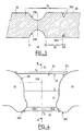
- Figure 1 shows the implementation of the invention. From a standard format card flat rectangular 20, length 8.5 cm; width 5.4 cm and thickness less than a millimeter, we perform the entire manufacturing process, including testing the micromodule 22 (once it has been put in place in the top left corner of the map, with flush contacts) and the personalization of card areas by printing of graphic texts.
- the mini-card 30 is not detached.
- a cutout is shown partial consisting of a slot 32 on all the thickness of the card.
- This slot 32 defines and extends around the periphery of the mini-card 30, except at some places where it is interrupted and leaves straps 34 and 40 connecting the reduced size card 30 to the rest of the standard format card 20.
- FIG 3 shows a sectional view along B-B a strap 34 shown in Figure 2.
- This strap 34 has two portions 35 and 36 in which it has a weakened thickness.
- a first portion 36, located on the side of the card of reduced format 30 is shaped to constitute a imposed place of rupture.
- This imposed place of rupture is constituted, in the example, by two notches 38A, 38B, conical, made respectively on the front and back sides of the card, and across the width 12 of the strap 34, as illustrated on the Figures 2 and 4. These notches are for example made on a depth of 150 ⁇ m on the front of the map (reference 38A), and over a depth of 120 ⁇ m on the back of the card (reference 38B).
- a second portion 35 located on the side of the standard format card 20, the thickness is thinned on both sides front 37A and back 37B. This thinning is achieved in particular by sinking a suitable tool in portion 35, on a sufficient depth, for example 250 ⁇ m, on each face of the card. It also extends over the entire width 11 of the strap as illustrated in the figure 2 and on the top view and enlarged of FIG. 4.
- this thinning 37A, 37B, in the portion 35 of the strap 34 preferably present a form of channel with a rounded profile.
- This shape rounded avoids the creation and spread of cracks during bending tests of the card. of the corners too sharp, such as in a trapezoidal shape for example, may not be suitable because they do not avoid not the spread of these cracks.
- This thinning 37A, 37B of the thickness of the strap 34 constitutes a hinge.
- Such a hinge has the function of ensuring decoupling mechanical between the card body and the first portion 36 shaped to constitute an imposed place of break. This prevents accidental breakage of the 34 suspenders and an involuntary separation from the mini-card 30.
- the hinge also has the function, during a voluntary pressure, for example with a finger on the mini-map 30, to move and focus the pressure constraints towards the imposed place of rupture (in the first portion 36), thus guaranteeing a rupture at this place rather than at another place of the ramp.
- the hinge can be obtained directly by injection in case the card and the slot to define the outline of the map at reduced format would be obtained by injection.
- the shape of the hinge can be equivalent to a rounded thinning as in Figure 3, or by example constitute a flexible blade meeting the pivot principle.
- the hinge could also be discontinued by two parts overlapping one another, the mini-map and the card body being fabricated independently each with a hinge part intended to be nested with the complementary part.
- the slot 32 then has two leaves of connection 37C, 38C which appear on each side of the strap 34 as illustrated in FIG. 2 and in the enlarged top view of Figure 4. So, in the map of the surface of the map located above and below portion 35 respectively reserved for thinning, the slot 32 has a first connection leave 37C to the format card standard 20; and in the map of the surface of the map located respectively above and below the portion 36 reserved for the imposed place of rupture, the slot 32 presents a second connecting leave 38C at the mini-map 30. The radius of curvature of the leave of 38C connection to the mini-card is lower than that connection leave 37C to the card body 20. From more, the strap 34 has a width 12, on the side of the reduced format card 30, which is less than width 11 on the side of the standard format card 20.
- the pressure forces on the mini-card are moved by the hinge (second portion 35) towards the zone 33, located between the two portions 35, 36 of the strap 34, and are concentrated at the level of the primer breaking (first portion 36), so it is possible to make a frank cut of the mini-card.
- the mini-card 30 thus obtained therefore has clean and regular edges.
- the smart card according to the invention can also have other types of suspenders. So she can for example have a large strap 40 which extends along a small side of the mini-map 30, as shown in the diagram in Figure 2.
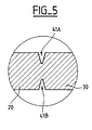
- the figure 5 shows a sectional view of this large strap referenced 40, whose width 13 is greater than that of the suspenders 34 previously described.
- This strap 40 actually has just an imposed place breaking formed by two notches 41A, 41B which extend over its entire width. These two cuts 41A, 41B are respectively carried out on the two front and back sides of the card.
- the slot 32 has two small leaves 42 at both ends of the strap 40. These holidays set back allow a good orientation of the constraints towards notches 41A, 41B when cutting the mini-card 30, by pressing a finger for example.
Landscapes
- Engineering & Computer Science (AREA)
- Computer Hardware Design (AREA)
- Microelectronics & Electronic Packaging (AREA)
- Physics & Mathematics (AREA)
- General Physics & Mathematics (AREA)
- Theoretical Computer Science (AREA)
- Credit Cards Or The Like (AREA)
- Purses, Travelling Bags, Baskets, Or Suitcases (AREA)
- Coupling Device And Connection With Printed Circuit (AREA)
Claims (10)
- Chipkarte im Standardformat mit einem Kartenkörper (20) und einer Minikarte (30), die über mindestens einen Steg (34) mit im verbunden ist, wobei der besagte Steg einen ersten Abschnitt (36) umfasst, der auf der Seite der Minikarte (30) angeordnet und ausgebildet ist, um eine Sollbruchstelle zu bilden, um eine Trennung der Minikarte (30) per Fingerdruck zu ermöglichen, dadurch gekennzeichnet, dass der besagte Steg (34) ebenfalls einen zweiten, vom ersten Abschnitt (36) getrennten Abschnitt (35) umfasst, der auf der Seite des Kartenkörpers (20) angeordnet ist und ein Scharnier bilden kann.
- Chipkarte nach Anspruch 1, dadurch gekennzeichnet, dass das besagte Scharnier aus einer Verdünnung (37A, 37B) der Dicke des Stegs (34) besteht.
- Chipkarte nach Anspruch 2, dadurch gekennzeichnet, dass die Verdünnung (37A, 37B) eine Rinnenform mit abgerundetem Profil aufweist.
- Chipkarte nach Anspruch 3, dadurch gekennzeichnet, dass die Verdünnung (37A, 27B) über eine Tiefe von 260 µm auf der Vorder- und der Rückseite der Karte hergestellt wird.
- Chipkarte nach einem der Ansprüche 1 bis 4, dadurch gekennzeichnet, dass die Sollbruchstelle aus zwei Kerben (38A, 38B) auf der Vorder- und Rückseite der Karte besteht.
- Chipkarte nach Anspruch 5, dadurch gekennzeichnet, dass die Kerben (38A, 38B) über eine Tiefe von 150 µm auf der Vorderseite (38A) und von 120 µm auf der Rückseite (38B) der Karte vorgesehen sind.
- Chipkarte nach einem der Ansprüche 1 bis 6, dadurch gekennzeichnet, dass der oder die Steg(e) (34) Hohlkehlen (37C, 38C) jeweils für den Anschluss an die Karte (20) und die Minikarte (30) umfasst (umfassen).
- Chipkarte nach einem der Ansprüche 1 bis 7, dadurch gekennzeichnet, dass die Breite (12) des Stegs (34) auf der Seite der Minikarte (30) kleiner ist als die Breite (11) des Stegs (34) auf der Seite des Kartenkörpers (20).
- Chipkarte nach einem der Ansprüche 1 bis 8, dadurch gekennzeichnet, dass sie ferner einen großen Steg (40) entlang einer Schmalseite der Minikarte (30) aufweist, und dass dieser große Steg eine Sollbruchstelle umfasst, die von zwei Kerben (41A, 41B) gebildet wird, die sich über seine ganze Breite und auf der Vorder- und Rückseite der Karte erstrecken.
- Herstellungsverfahren einer kleinformatigen Chipkarte (30), das das gesamte Fertigungsverfahren einer Chipkarte im Standardformat (20) umfasst, sowie eine zusätzliche Etappe zur Herstellung eines Teilausschnitts mit den Abmessungen der Minikarte (30), wobei der besagte Teilausschnitt aus einem örtlich von mindestens einem Steg (34) zwischen der kleinformatigen Karte (30) und der Karte im Standardformat (20) unterbrochenen Schlitz (32) besteht, dadurch gekennzeichnet, dass der oder die Steg(e) so beschaffen ist (sind), dass er (sie) einen ersten Abschnitt (36) umfasst (umfassen), der auf der Seite der Minikarte (30) angeordnet und ausgebildet ist, um eine Sollbruchstelle zu bilden, und einen zweiten, vom ersten Abschnitt (36) getrennten Abschnitt (35), der auf der Seite der Karte im Standardformat (20) angeordnet ist und aus einer Verdünnung der Dicke des Stegs (der Stege) besteht, wobei der besagte erste und zweite Abschnitt über die ganze Breite des Stegs (der Stege) und auf der Vorder- und Rückseite der Karte vorgesehen sind.
Applications Claiming Priority (3)
| Application Number | Priority Date | Filing Date | Title |
|---|---|---|---|
| FR9811971A FR2783948B1 (fr) | 1998-09-24 | 1998-09-24 | Carte a puce grand format comprenant une mini-carte detachable et procede de fabrication |
| FR9811971 | 1998-09-24 | ||
| PCT/FR1999/002071 WO2000017814A1 (fr) | 1998-09-24 | 1999-08-31 | Carte a puce grand format comprenant une mini-carte detachable et procede de fabrication |
Publications (2)
| Publication Number | Publication Date |
|---|---|
| EP1116178A1 EP1116178A1 (de) | 2001-07-18 |
| EP1116178B1 true EP1116178B1 (de) | 2002-11-27 |
Family
ID=9530815
Family Applications (1)
| Application Number | Title | Priority Date | Filing Date |
|---|---|---|---|
| EP99940259A Expired - Lifetime EP1116178B1 (de) | 1998-09-24 | 1999-08-31 | Standardformatige ic-karte mit einer abnehmbaren mini-karte und herstellungsverfahren |
Country Status (9)
| Country | Link |
|---|---|
| US (1) | US6685097B1 (de) |
| EP (1) | EP1116178B1 (de) |
| CN (1) | CN1157690C (de) |
| AT (1) | ATE228687T1 (de) |
| AU (1) | AU5427299A (de) |
| DE (1) | DE69904219T2 (de) |
| ES (1) | ES2188219T3 (de) |
| FR (1) | FR2783948B1 (de) |
| WO (1) | WO2000017814A1 (de) |
Families Citing this family (39)
| Publication number | Priority date | Publication date | Assignee | Title |
|---|---|---|---|---|
| FR2817063A1 (fr) * | 2000-11-20 | 2002-05-24 | Roberge Dominique | Carte a memoire electronique microsim |
| FR2826155B1 (fr) * | 2001-06-14 | 2003-09-19 | Oberthur Card Syst Sa | Carte a microcircuit avec plaquette detachable |
| FR2829267B1 (fr) | 2001-09-05 | 2003-12-12 | Gemplus Card Int | Carte du type carte a puce comprenant un support plan sensiblement rectangulaire |
| FR2853434B1 (fr) * | 2003-04-03 | 2005-07-01 | Oberthur Card Syst Sa | Carte a microcircuit fixee sur un support adaptateur, support de carte et procede de fabrication |
| US7341198B2 (en) * | 2004-02-20 | 2008-03-11 | Renesas Technology Corp. | IC card and a method of manufacturing the same |
| FR2872946B1 (fr) * | 2004-07-08 | 2006-09-22 | Gemplus Sa | Procede de fabrication d'un support de carte a puce mini uicc avec adaptateur plug-in uicc associe et support obtenu |
| US20060118639A1 (en) * | 2004-12-06 | 2006-06-08 | First Data Corporation | Punchout contactless transaction card |
| EP1684213A1 (de) * | 2005-01-18 | 2006-07-26 | Arthur Blank & Company, Inc. | Verfahren zum Herstellen einer Transaktionskartenanordnung |
| JP2007183776A (ja) * | 2006-01-06 | 2007-07-19 | Renesas Technology Corp | 半導体装置 |
| US20070176007A1 (en) * | 2006-01-31 | 2007-08-02 | Priya Suresh C | Variably sized mini card |
| US8123135B2 (en) * | 2006-09-08 | 2012-02-28 | Mastercard International, Inc. | Very small subcard for identification applications |
| US7997498B2 (en) | 2006-09-08 | 2011-08-16 | Mastercard International, Inc. | Identification of installable card |
| US7991692B2 (en) | 2006-10-09 | 2011-08-02 | First Data Corporation | Electronic payment instrument and packaging |
| US8794532B2 (en) * | 2008-12-29 | 2014-08-05 | Mastercard International Incorporated | Methods and apparatus for use in association with identification token |
| US8286862B2 (en) * | 2007-12-28 | 2012-10-16 | Mastercard International, Inc. | Methods and apparatus for use in association with security parameter |
| DE102008021519B3 (de) * | 2008-04-30 | 2009-10-01 | Giesecke & Devrient Gmbh | Sicherheitselement mit IC-Karte |
| US7885878B2 (en) * | 2008-05-28 | 2011-02-08 | First Data Corporation | Systems and methods of payment account activation |
| US8684261B2 (en) * | 2009-01-20 | 2014-04-01 | Mastercard International Incorporated | Methods, apparatus, computer program products and articles for use in providing human understandable indication of account balance |
| FR2958208B1 (fr) | 2010-03-30 | 2012-08-31 | Oberthur Technologies | Support comprenant un element detachable, procede de detachement d'un tel element detachable et procede de fabrication d'un tel support |
| SK288650B6 (sk) * | 2010-05-10 | 2019-03-01 | Smk Corporation | Nosič pamäťovej karty, spôsob prvotného ukladania dát do pamäťovej karty |
| FR2964219B1 (fr) * | 2010-08-24 | 2012-09-21 | Oberthur Technologies | Carte a microcircuit comprenant une mini-carte |
| CH703738B1 (de) | 2010-08-31 | 2018-05-31 | Swisscom Ag | SIM-Karte und Verfahren zur Herstellung derselben. |
| EP2587412A1 (de) * | 2011-10-31 | 2013-05-01 | Gemalto SA | Vorgestanzte Chipkarte |
| USD691610S1 (en) * | 2011-11-07 | 2013-10-15 | Blackberry Limited | Device smart card |
| US8950681B2 (en) | 2011-11-07 | 2015-02-10 | Blackberry Limited | Universal integrated circuit card apparatus and related methods |
| ITMI20112415A1 (it) | 2011-12-28 | 2013-06-29 | St Microelectronics Srl | Modulo sim |
| FR2985345B1 (fr) * | 2011-12-29 | 2021-11-26 | Oberthur Technologies | Procede de fabrication d'une carte de petite epaisseur detachable d'une plaque de grande epaisseur |
| EP2738714A1 (de) * | 2012-11-30 | 2014-06-04 | Gemalto SA | Herstellungsverfahren einer elektrischen oder elektronischen Vorrichtung mit einer Schnittstelle für die Stromversorgung oder Kommunikation |
| FR2999753B1 (fr) * | 2012-12-13 | 2015-02-13 | Oberthur Technologies | Procede de fabrication par lamination en continu de cartes a microcircuit du type a contact |
| US10027089B2 (en) | 2013-03-13 | 2018-07-17 | Hewlett Packard Enterprise Development Lp | Coupled ring resonator system |
| JP2015060392A (ja) | 2013-09-18 | 2015-03-30 | 株式会社東芝 | Icカード用基材、icカードの製造方法、及びicカード |
| FR3015087B1 (fr) | 2013-12-13 | 2017-05-12 | Plastifrance | Support de cartes de formats multiples et a positionnement reversible stable. |
| JP6342219B2 (ja) | 2014-05-27 | 2018-06-13 | 株式会社東芝 | Icカード用基材、及び嵌込icカード |
| USD1002717S1 (en) | 2021-12-01 | 2023-10-24 | Capital One Services, Llc | Transaction card |
| US11868833B2 (en) | 2021-12-01 | 2024-01-09 | Capital One Services, Llc | Transaction card assembly |
| US11893443B2 (en) | 2021-12-01 | 2024-02-06 | Capital One Services, Llc | Transaction card assembly |
| US11934900B2 (en) | 2021-12-01 | 2024-03-19 | Capital One Services, Llc | Transaction card assembly |
| US11907786B2 (en) | 2021-12-01 | 2024-02-20 | Capital One Services, Llc | Transaction card assembly |
| US11893573B2 (en) | 2021-12-01 | 2024-02-06 | Capital One Services, Llc | Transaction card assembly |
Family Cites Families (8)
| Publication number | Priority date | Publication date | Assignee | Title |
|---|---|---|---|---|
| DE3420051A1 (de) * | 1984-05-29 | 1985-12-05 | GAO Gesellschaft für Automation und Organisation mbH, 8000 München | Datentraeger mit ic-baustein und verfahren zur herstellung eines derartigen datentraegers |
| JPS62214998A (ja) * | 1986-03-17 | 1987-09-21 | 三菱電機株式会社 | 薄型半導体カ−ド |
| DE4007221A1 (de) * | 1990-03-07 | 1991-09-12 | Gao Ges Automation Org | Pruefkopf fuer kontaktflaechen von wertkarten mit eingelagertem halbleiterchip |
| FR2678753B1 (fr) | 1991-07-02 | 1996-12-20 | Gemplus Card Int | Fabrication de cartes a puce a module autodetachable. |
| US5581065A (en) * | 1993-08-02 | 1996-12-03 | Dai Nippon Printing Co., Ltd. | Sheet-framed IC carrier, method for producing the same, and IC carrier case |
| DE19606789C2 (de) * | 1996-02-23 | 1998-07-09 | Orga Kartensysteme Gmbh | Kunststoffkarte mit aus dieser heraustrennbarer Minichipkarte |
| FR2773900B1 (fr) * | 1998-01-22 | 2000-02-18 | Gemplus Card Int | Carte a circuit(s) integre(s) a contact, comportant une minicarte detachable |
| DE19901965A1 (de) * | 1999-01-19 | 2000-07-20 | Giesecke & Devrient Gmbh | Tragbarer Datenträger mit ausbrechbarer Minichipkarte |
-
1998
- 1998-09-24 FR FR9811971A patent/FR2783948B1/fr not_active Expired - Fee Related
-
1999
- 1999-08-31 EP EP99940259A patent/EP1116178B1/de not_active Expired - Lifetime
- 1999-08-31 CN CNB998113115A patent/CN1157690C/zh not_active Expired - Lifetime
- 1999-08-31 US US09/787,815 patent/US6685097B1/en not_active Expired - Lifetime
- 1999-08-31 AU AU54272/99A patent/AU5427299A/en not_active Abandoned
- 1999-08-31 ES ES99940259T patent/ES2188219T3/es not_active Expired - Lifetime
- 1999-08-31 AT AT99940259T patent/ATE228687T1/de not_active IP Right Cessation
- 1999-08-31 DE DE69904219T patent/DE69904219T2/de not_active Expired - Lifetime
- 1999-08-31 WO PCT/FR1999/002071 patent/WO2000017814A1/fr active IP Right Grant
Also Published As
| Publication number | Publication date |
|---|---|
| ATE228687T1 (de) | 2002-12-15 |
| CN1319215A (zh) | 2001-10-24 |
| FR2783948A1 (fr) | 2000-03-31 |
| WO2000017814A1 (fr) | 2000-03-30 |
| EP1116178A1 (de) | 2001-07-18 |
| FR2783948B1 (fr) | 2000-11-10 |
| AU5427299A (en) | 2000-04-10 |
| CN1157690C (zh) | 2004-07-14 |
| DE69904219T2 (de) | 2003-10-09 |
| US6685097B1 (en) | 2004-02-03 |
| DE69904219D1 (de) | 2003-01-09 |
| ES2188219T3 (es) | 2003-06-16 |
Similar Documents
| Publication | Publication Date | Title |
|---|---|---|
| EP1116178B1 (de) | Standardformatige ic-karte mit einer abnehmbaren mini-karte und herstellungsverfahren | |
| EP1886264B1 (de) | Klebender formatadapter für eine speichervorrichtung und verfahren zu seiner herstellung | |
| CA2429435C (fr) | Carte a puce sans contact ou hybride contact-sans contact a tenue renforcee du module electronique | |
| EP0521778B1 (de) | Herstellung von Chipkarten mit selbstlösbarem Modull | |
| EP1769429B1 (de) | Verfahren zur herstellung eines mini-uicc-chipkarten-trägers mit einem assoziierten plug-in-uicc-adapter und so erhaltene halterung | |
| EP1192594B1 (de) | Herstellungsverfahren einer laminierten karte mit einer zwischenschicht aus petg | |
| EP2036007B1 (de) | Verfahren zum herstellen von karten, die jeweils ein elektronisches modul umfassen, und zwischenprodukte | |
| FR2964063A1 (fr) | Procede de fabrication d'une carte a partir d'un support | |
| EP1105839B1 (de) | Verfahren zum herstellen einer kontaktlosen chipkarte | |
| FR2794059A1 (fr) | Dispositif portable a circuit integre et procede de fabrication | |
| EP1433127B1 (de) | Chip-karte mit einem rechteckigen flächigen träger | |
| EP1214685B1 (de) | Biegesteifte karte mit trennbarem modul | |
| EP1073998B1 (de) | Verfahren zur herstellung einer mit kontakten versehenen ic-karte und nach diesem verfahren hergestellte ic-karte | |
| EP1611813B1 (de) | Epilierstreifen für Epilierung mit Epilierwachs | |
| EP1080446B1 (de) | Zwei-standard ic-karte mit einem isolierungsschlitz | |
| EP2587412A1 (de) | Vorgestanzte Chipkarte | |
| WO2013098508A1 (fr) | Adaptateur de format pour carte a cote convexe | |
| EP2521073B1 (de) | Vorbereitungsverfahen eines Kartenhalters auf Zellulosebasis für Minikarte | |
| EP2423857B1 (de) | Mikrochipkarte, die eine Minikarte umfasst | |
| EP2766854B1 (de) | Verfahren und vorrichtung zur herstellung eines substrats zur aufnahme einer elektronischen vorrichtung und substrat | |
| FR3131035A1 (fr) | Support de carte SIM et éjecteur de carte SIM | |
| FR3090447A1 (fr) | Procédé de réalisation d’un contour d’un élément détachable dans un substrat, dispositif et substrat associés | |
| WO2014083002A1 (fr) | Procede de fabrication de dispositif electrique ou electronique a interface d'alimentation ou de communication | |
| FR2819081A1 (fr) | Carte a puce a structure composee et procede de fabrication | |
| FR2967515A1 (fr) | Carte a microcircuit a au moins trois formats de mise en oeuvre |
Legal Events
| Date | Code | Title | Description |
|---|---|---|---|
| PUAI | Public reference made under article 153(3) epc to a published international application that has entered the european phase |
Free format text: ORIGINAL CODE: 0009012 |
|
| 17P | Request for examination filed |
Effective date: 20010424 |
|
| AK | Designated contracting states |
Kind code of ref document: A1 Designated state(s): AT BE CH CY DE DK ES FI FR GB GR IE IT LI LU MC NL PT SE |
|
| GRAG | Despatch of communication of intention to grant |
Free format text: ORIGINAL CODE: EPIDOS AGRA |
|
| RTI1 | Title (correction) |
Free format text: STANDART FORMAT SMART CARD COMPRISING A REMOVABLE MINICARD AND METHOD FOR MAKING SAME |
|
| RTI1 | Title (correction) |
Free format text: STANDARD FORMAT SMART CARD COMPRISING A REMOVABLE MINICARD AND METHOD FOR MAKING SAME |
|
| 17Q | First examination report despatched |
Effective date: 20010827 |
|
| GRAG | Despatch of communication of intention to grant |
Free format text: ORIGINAL CODE: EPIDOS AGRA |
|
| GRAH | Despatch of communication of intention to grant a patent |
Free format text: ORIGINAL CODE: EPIDOS IGRA |
|
| GRAH | Despatch of communication of intention to grant a patent |
Free format text: ORIGINAL CODE: EPIDOS IGRA |
|
| GRAA | (expected) grant |
Free format text: ORIGINAL CODE: 0009210 |
|
| AK | Designated contracting states |
Kind code of ref document: B1 Designated state(s): AT BE CH CY DE DK ES FI FR GB GR IE IT LI LU MC NL PT SE |
|
| PG25 | Lapsed in a contracting state [announced via postgrant information from national office to epo] |
Ref country code: NL Free format text: LAPSE BECAUSE OF FAILURE TO SUBMIT A TRANSLATION OF THE DESCRIPTION OR TO PAY THE FEE WITHIN THE PRESCRIBED TIME-LIMIT Effective date: 20021127 Ref country code: IE Free format text: LAPSE BECAUSE OF FAILURE TO SUBMIT A TRANSLATION OF THE DESCRIPTION OR TO PAY THE FEE WITHIN THE PRESCRIBED TIME-LIMIT Effective date: 20021127 Ref country code: GR Free format text: LAPSE BECAUSE OF FAILURE TO SUBMIT A TRANSLATION OF THE DESCRIPTION OR TO PAY THE FEE WITHIN THE PRESCRIBED TIME-LIMIT Effective date: 20021127 Ref country code: FI Free format text: LAPSE BECAUSE OF FAILURE TO SUBMIT A TRANSLATION OF THE DESCRIPTION OR TO PAY THE FEE WITHIN THE PRESCRIBED TIME-LIMIT Effective date: 20021127 Ref country code: AT Free format text: LAPSE BECAUSE OF FAILURE TO SUBMIT A TRANSLATION OF THE DESCRIPTION OR TO PAY THE FEE WITHIN THE PRESCRIBED TIME-LIMIT Effective date: 20021127 |
|
| REF | Corresponds to: |
Ref document number: 228687 Country of ref document: AT Date of ref document: 20021215 Kind code of ref document: T |
|
| REG | Reference to a national code |
Ref country code: GB Ref legal event code: FG4D Free format text: NOT ENGLISH |
|
| REG | Reference to a national code |
Ref country code: CH Ref legal event code: EP |
|
| REG | Reference to a national code |
Ref country code: IE Ref legal event code: FG4D Free format text: FRENCH |
|
| REF | Corresponds to: |
Ref document number: 69904219 Country of ref document: DE Date of ref document: 20030109 |
|
| PG25 | Lapsed in a contracting state [announced via postgrant information from national office to epo] |
Ref country code: SE Free format text: LAPSE BECAUSE OF FAILURE TO SUBMIT A TRANSLATION OF THE DESCRIPTION OR TO PAY THE FEE WITHIN THE PRESCRIBED TIME-LIMIT Effective date: 20030227 Ref country code: PT Free format text: LAPSE BECAUSE OF FAILURE TO SUBMIT A TRANSLATION OF THE DESCRIPTION OR TO PAY THE FEE WITHIN THE PRESCRIBED TIME-LIMIT Effective date: 20030227 Ref country code: DK Free format text: LAPSE BECAUSE OF FAILURE TO SUBMIT A TRANSLATION OF THE DESCRIPTION OR TO PAY THE FEE WITHIN THE PRESCRIBED TIME-LIMIT Effective date: 20030227 |
|
| GBT | Gb: translation of ep patent filed (gb section 77(6)(a)/1977) |
Effective date: 20030317 |
|
| NLV1 | Nl: lapsed or annulled due to failure to fulfill the requirements of art. 29p and 29m of the patents act | ||
| REG | Reference to a national code |
Ref country code: ES Ref legal event code: FG2A Ref document number: 2188219 Country of ref document: ES Kind code of ref document: T3 |
|
| REG | Reference to a national code |
Ref country code: IE Ref legal event code: FD4D Ref document number: 1116178E Country of ref document: IE |
|
| PG25 | Lapsed in a contracting state [announced via postgrant information from national office to epo] |
Ref country code: MC Free format text: LAPSE BECAUSE OF NON-PAYMENT OF DUE FEES Effective date: 20030831 Ref country code: LU Free format text: LAPSE BECAUSE OF NON-PAYMENT OF DUE FEES Effective date: 20030831 Ref country code: LI Free format text: LAPSE BECAUSE OF NON-PAYMENT OF DUE FEES Effective date: 20030831 Ref country code: CY Free format text: LAPSE BECAUSE OF FAILURE TO SUBMIT A TRANSLATION OF THE DESCRIPTION OR TO PAY THE FEE WITHIN THE PRESCRIBED TIME-LIMIT Effective date: 20030831 Ref country code: CH Free format text: LAPSE BECAUSE OF NON-PAYMENT OF DUE FEES Effective date: 20030831 Ref country code: BE Free format text: LAPSE BECAUSE OF NON-PAYMENT OF DUE FEES Effective date: 20030831 |
|
| PLBE | No opposition filed within time limit |
Free format text: ORIGINAL CODE: 0009261 |
|
| STAA | Information on the status of an ep patent application or granted ep patent |
Free format text: STATUS: NO OPPOSITION FILED WITHIN TIME LIMIT |
|
| 26N | No opposition filed |
Effective date: 20030828 |
|
| BERE | Be: lapsed |
Owner name: *GEMPLUS Effective date: 20030831 |
|
| REG | Reference to a national code |
Ref country code: CH Ref legal event code: PL |
|
| REG | Reference to a national code |
Ref country code: FR Ref legal event code: TP Ref country code: FR Ref legal event code: CD |
|
| REG | Reference to a national code |
Ref country code: GB Ref legal event code: 732E Free format text: REGISTERED BETWEEN 20100916 AND 20100922 |
|
| REG | Reference to a national code |
Ref country code: GB Ref legal event code: 732E Free format text: REGISTERED BETWEEN 20110616 AND 20110622 |
|
| REG | Reference to a national code |
Ref country code: DE Ref legal event code: R082 Ref document number: 69904219 Country of ref document: DE Representative=s name: HOFFMANN - EITLE, DE |
|
| REG | Reference to a national code |
Ref country code: DE Ref legal event code: R082 Ref document number: 69904219 Country of ref document: DE Representative=s name: HOFFMANN - EITLE PATENT- UND RECHTSANWAELTE PA, DE Effective date: 20120629 Ref country code: DE Ref legal event code: R082 Ref document number: 69904219 Country of ref document: DE Representative=s name: HOFFMANN - EITLE, DE Effective date: 20120629 Ref country code: DE Ref legal event code: R081 Ref document number: 69904219 Country of ref document: DE Owner name: GEMALTO SA, FR Free format text: FORMER OWNER: GEMPLUS, GEMENOS, FR Effective date: 20120629 |
|
| REG | Reference to a national code |
Ref country code: FR Ref legal event code: PLFP Year of fee payment: 18 |
|
| REG | Reference to a national code |
Ref country code: FR Ref legal event code: PLFP Year of fee payment: 19 |
|
| REG | Reference to a national code |
Ref country code: FR Ref legal event code: PLFP Year of fee payment: 20 |
|
| PGFP | Annual fee paid to national office [announced via postgrant information from national office to epo] |
Ref country code: IT Payment date: 20180719 Year of fee payment: 20 Ref country code: FR Payment date: 20180720 Year of fee payment: 20 Ref country code: DE Payment date: 20180719 Year of fee payment: 20 Ref country code: ES Payment date: 20180903 Year of fee payment: 20 |
|
| PGFP | Annual fee paid to national office [announced via postgrant information from national office to epo] |
Ref country code: GB Payment date: 20180720 Year of fee payment: 20 |
|
| REG | Reference to a national code |
Ref country code: DE Ref legal event code: R071 Ref document number: 69904219 Country of ref document: DE |
|
| REG | Reference to a national code |
Ref country code: GB Ref legal event code: PE20 Expiry date: 20190830 |
|
| PG25 | Lapsed in a contracting state [announced via postgrant information from national office to epo] |
Ref country code: GB Free format text: LAPSE BECAUSE OF EXPIRATION OF PROTECTION Effective date: 20190830 |
|
| REG | Reference to a national code |
Ref country code: ES Ref legal event code: FD2A Effective date: 20200904 |
|
| PG25 | Lapsed in a contracting state [announced via postgrant information from national office to epo] |
Ref country code: ES Free format text: LAPSE BECAUSE OF EXPIRATION OF PROTECTION Effective date: 20190901 |