EP1102526A2 - Montagesystem für die reihenweise Montage von Steckeinschüben - Google Patents
Montagesystem für die reihenweise Montage von Steckeinschüben Download PDFInfo
- Publication number
- EP1102526A2 EP1102526A2 EP00125138A EP00125138A EP1102526A2 EP 1102526 A2 EP1102526 A2 EP 1102526A2 EP 00125138 A EP00125138 A EP 00125138A EP 00125138 A EP00125138 A EP 00125138A EP 1102526 A2 EP1102526 A2 EP 1102526A2
- Authority
- EP
- European Patent Office
- Prior art keywords
- plug
- modules
- connector
- drives
- mating
- Prior art date
- Legal status (The legal status is an assumption and is not a legal conclusion. Google has not performed a legal analysis and makes no representation as to the accuracy of the status listed.)
- Granted
Links
- 230000013011 mating Effects 0.000 claims abstract description 48
- 238000003780 insertion Methods 0.000 claims description 5
- 230000037431 insertion Effects 0.000 claims description 5
- 238000011144 upstream manufacturing Methods 0.000 claims 1
- 238000009434 installation Methods 0.000 abstract description 8
- BZTYNSQSZHARAZ-UHFFFAOYSA-N 2,4-dichloro-1-(4-chlorophenyl)benzene Chemical compound C1=CC(Cl)=CC=C1C1=CC=C(Cl)C=C1Cl BZTYNSQSZHARAZ-UHFFFAOYSA-N 0.000 description 1
- 102100032131 Lymphocyte antigen 6E Human genes 0.000 description 1
- 101710157879 Lymphocyte antigen 6E Proteins 0.000 description 1
- 238000000034 method Methods 0.000 description 1
- 239000013307 optical fiber Substances 0.000 description 1
Images


Classifications
-
- H—ELECTRICITY
- H05—ELECTRIC TECHNIQUES NOT OTHERWISE PROVIDED FOR
- H05K—PRINTED CIRCUITS; CASINGS OR CONSTRUCTIONAL DETAILS OF ELECTRIC APPARATUS; MANUFACTURE OF ASSEMBLAGES OF ELECTRICAL COMPONENTS
- H05K7/00—Constructional details common to different types of electric apparatus
- H05K7/14—Mounting supporting structure in casing or on frame or rack
- H05K7/1438—Back panels or connecting means therefor; Terminals; Coding means to avoid wrong insertion
- H05K7/1439—Back panel mother boards
Definitions
- the present invention relates to a mounting system for the installation of plug-in modules in rows with in the direction of the row different, predetermined dimensions in one electronic device, the plug-in modules each via a back on its leading in the direction of insertion arranged connector with one of the on the back plate (backplane) of the device in a row in a row arranged mating connector can be coupled.
- plug-in modules have different dimensions can, it is generally required to have a slot dimensioned so that the largest one in question Plug-in slot has space. If then with a plug-in module smaller dimensions, part of the Unused space.
- a typical example of the latter case are computers, into the multiple hard drives in a row can be installed one above the other.
- the present invention is illustrated wherein however, this is not limited to this, but also others Plug-in modules and, for example, an arrangement the plug-in modules are sensed side by side.
- Server and attached storage expansion units are increasingly using hot-swappable hard drives equipped. This can result in redundant configurations a failed hard drive can be replaced, without having to shut down the system.
- Hard drives are generally of two different types Height dimensions available, namely with a Height of 1 "or a height of 1.6"; the remaining dimensions, i.e. So width and depth, are with both types of drives equal.
- a back plate for 1.6 "drives can be provided, so it can also be used of 1 "drives only four such drives are inserted; also in this case, a considerable space remains unused.
- This object is achieved in that the Mating connector on the back plate with one of the smallest specified Dimension of the possible plug-in modules corresponding Pitch are arranged, and that at least the plug-in modules with a larger dimension at least two in a row, have plugs connected in parallel, the Distance smaller than the pitch of the mating connector is.
- This arrangement allows for such a equipped with several plugs Finding plug positions, each with one of its Plug with a mating connector is aligned, so that for the arrangement of the plug-in modules a wider range results.
- This arrangement also allows the plug-in units with a to assemble a wider range of arrangements and in the event that the plug of a plug-in module is not a mating connector on the back plate, the distance from the plug to a free mating plug using the Bridge adapters.
- the adapters are each one to the direction of insertion include transverse PCB, on the insertion side Surface of the input connector and on their one or more in the row direction Output connectors arranged one behind the other are provided are whose axes lie in a common plane.
- the circuit board contains the connecting lines between the input connector and the output connector. Circuit boards are inexpensive to produce in a simple manner, so that on adapters manufactured in this way can be inexpensive.
- the adapter always has one input connector and several Output connector; the axis of the input connector according to an embodiment between the axes of two output plugs run, as with an exemplary embodiment is set out, or the axes of the output connector can turn into a relative to the axis of the input connector Be offset, as not shown.
- the mating connector the spacing of the back plate the first given height dimension, and the connector or output plugs are spaced from each other, which is half the pitch of the mating connector corresponds.
- the plug-in modules can then be arranged in this way be that one of the two plugs of the plug-in module or output connector of the adapter to a mating connector the back plate is aligned, making a space-saving Arrangement of hard drives of different thicknesses is possible.
- At least one status signal lamp for each mating connector on the rear panel is assigned, and that each plug-in module from the front to the back Light guide is assigned, the back side end according to the number of plugs or output plugs of the adapter assigned to the plug-in module. So if an adapter with two output plugs is provided, then the light guide is on his rear end branched into two branches so that each State signal lamp is assigned an optical fiber end.
- the drives 4 are each with a recessed plug 6 equipped, each in one the rear plate 2 arranged mating connector 8 engages.
- the drives 4 are each arranged in a frame 10, which in a known manner in the not shown Computer housing can be used so that the Drive is correctly placed and held firmly.
- the mating connectors 8 have one Pitch a, which is based on the thickness dimension of the Drives is matched.
- FIG. 2 shows a rear plate in a view similar to FIG. 1 12, on which four 1.6 "drives 14 are mounted Drives 14 are on their plugs 16 with the back plate 12 arranged mating connectors 18 electrically connected.
- the drives 14 are also adapted to their size Frame 20 added, which in turn in the housing of the computer.
- the mating connector 18 have a pitch b in the case of FIG. 2, which is adapted to the thickness of the 1.6 "drives, i.e., b is larger than a.
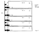
- Fig. 3 shows a back plate 22, in which both the mating connectors 8 according to the Fig. 1 corresponding mating connector 8 'and the mating connector 18 of FIG. 2 corresponding mating connector 18 'is provided are, for example, that shown in Fig. 3 Allow arrangement.
- FIG. 3 would be an arrangement is also possible in which three 1 "drives are arranged over two 1.6 "drives.
- Fig. 4 shows a drive arrangement according to the invention accordingly 3.
- three 1 "drives and in the upper half of the Installation frame two 1.6 "drives arranged.
- the back plate 2 with the mating connectors 8 corresponds exactly to the mating plate 2 of FIG. 1.
- the lower drives 4 can directly as in the case of FIG. 1 be plugged in, i.e. the connectors 6 take the mating connector 8, so that extensions as in the case of Fig. 3rd are not required.
- Adapter 26 In the plug 16 of the upper drives 14 is one Adapter 26 inserted, which is the connection to one of the Mating connector 8 produces.
- the two adapters 26 are each other equal. They each have a parallel to the back plate 8 PCB 28 on the drive side Surface an input connector 30 is arranged, and at the rear panel-side surface two output connectors 32, 34 arranged are.
- the configuration of the adapter 26 according to FIG. 4 is accordingly given the opportunity to arrange the drive 14 so that its connector is either at a distance of 1/4 a below the next higher mating connector or at a distance 1/4 a above the next lower mating connector is, so that compared to the fundamentally existing Possibility of aligning the connector 16 to one Align mating connector, two further arrangements realized can be.
- each mating connector 8 is the Back plate 2 each assigned a status signal lamp 9, which has a specific operating state of the mating connector displays. It is well known, the light of this Status signal lamps via one on the frame or on Drive attached light guide from the back plate to the To lead the front of the drives, such as at the drives 4 in Fig. 4 can be seen.
- the light guide 4 takes the light coming from the status signal lamp 9 and leads it to the front end 13 of the light guide 11.
- the assigned light guide is also in a corresponding number of arms branched.
Landscapes
- Engineering & Computer Science (AREA)
- Microelectronics & Electronic Packaging (AREA)
- Details Of Connecting Devices For Male And Female Coupling (AREA)
- Coupling Device And Connection With Printed Circuit (AREA)
- Two-Way Televisions, Distribution Of Moving Picture Or The Like (AREA)
- Conveying And Assembling Of Building Elements In Situ (AREA)
Abstract
Description
- Fig. 1
- zeigt schematisch eine Anordnung von mehreren 1"-Laufwerken an einer Rückplatte gemäß dem Stand der Technik;
- Fig. 2
- zeigt schematisch die Anordnung von mehreren 1,6-"Laufwerken an einer Rückplatte gemäß dem Stand der Technik;
- Fig. 3
- zeigt schematisch die Anordnung von mehreren 1"-Laufwerken und mehreren 1,6-"-Laufwerken an einer Rückwand gemäß dem Stand der Technik;
- Fig. 4
- zeigt schematisch die Anordnung von mehreren 1"-Laufwerken und mehreren 1,6"-Laufwerken an einer Rückplatte gemäß der Erfindung.
Claims (7)
- Montagesystem für die reihenweise Montage von Steckeinschüben mit in Reihenrichtung unterschiedlichen, vorgegebenen Abmessungen in einem elektronischen Gerät, wobei die Steckeinschübe jeweils über einen an ihrer in Einschubrichtung voreilenden Rückseite angeordneten Stecker mit einem der an der Rückplatte (backplane) des Gerätes in Reihenrichtung hintereinander angeordneten Gegenstekker gekuppelt werden, dadurch gekennzeichnet, daß die Gegenstecker (8) an der Rückplatte (2) mit einem der kleinsten vorgegebenen Abmessung der Steckeinschübe (4) entsprechenden Teilungsabstand (a) angeordnet sind, und daß zumindest die Steckeinschübe (14) mit größerer Abmessung jeweils wenigstens zwei in Reihenrichtung hintereinander angeordnete, zueinander parallel gschaltete Stecker (32, 43) aufweisen, deren Abstand (c) kleiner als der Teilungsabstand (a) der Gegenstecker (8) ist.
- Montagesystem nach Anspruch 1, dadurch gekennzeichnet, daß die parallel geschalteten Stecker (32, 34) der Stekkeinschübe (14) jeweils durch einen Adapter (26) gebildet sind, welcher einen mit einem einzigen vorgesehenen Stecker (16) des Steckeinschubes (14) kuppelbaren Eingangsstecker (30) und wenigstens zwei Ausgangsstecker (32, 34) hat, die mit dem Eingangsstecker (16) verbunden und zueinander parallel geschaltet sind, und die mit jeweils einem Gegenstecker (8) der Rückplatte (2) kuppelbar sind.
- Montagesystem nach Anspruch 2, dadurch gekennzeichnet, daß die Adapter (26) jeweils eine zur Steckrichtung quer stehende Leiterplatte (28) umfassen, auf deren einschubseitiger Fläche der Eingangsstecker (16) und auf deren rückplattenseitiger Fläche die Ausgangsstecker (32, 34) angeordnet sind.
- Montagesystem nach den Ansprüchen 2 oder 3, dadurch gekennzeichnet, daß die Achsen der Ausgangsstecker zu einer Seite der Achse des Eingangssteckers hin versetzt angeordnet sind.
- Montagesystem nach den Ansprüchen 2 oder 3, dadurch gekennzeichnet, daß die Achse des Eingangssteckers (16) zwischen den Achsen zweier in Reihenrichtung davor bzw. dahinter angeordneten Ausgangssteckern (32, 34) angeordnet ist.
- Montagesystem nach einem der Ansprüche 1 bis 5, dadurch gekennzeichnet, daß für die Übereinander-Montage von ersten Steckeinschüben (4) mit einer kleineren Höhe (1") und von zweiten Steckeinschüben (14) mit einer größeren Höhe (1,6") die Gegenstecker (8) der Rückplatte (2) einen Teilungsabstand (a) haben, welcher an die kleinere Höhe (1") angepaßt ist, und daß die Steckeinschübe (14) mit der größeren Höhe (1,6") jeweils zwei übereinander angeordnete Stecker (32, 34) haben, deren Abstand (c) der Hälfte des Teilungsabstandes (a) der Gegenstecker (8) entspricht.
- Montagesystem nach einem der Ansprüche 1 bis 6, dadurch gekennzeichnet, daß jedem Gegenstecker (8) der Rückplatte wenigstens eine Zustands-Signallampe (9) zugeordnet ist, und daß jedem Steckeinschub (14) ein von der Vorderseite desselben zur Rückseite verlaufender Lichtleiter (15) zugeordnet ist, welcher sich entsprechend der Anzahl der an den Steckeinschüben größeren Abmessung vorgesehenen Stecker bzw. der Ausgangsstecker (32, 34) des dem Steckeinschub (14) zugeordneten Adapters (26) verzweigt.
Applications Claiming Priority (2)
| Application Number | Priority Date | Filing Date | Title |
|---|---|---|---|
| DE19955783 | 1999-11-19 | ||
| DE19955783A DE19955783C2 (de) | 1999-11-19 | 1999-11-19 | Montagesystem für die reihenweise Montage von Steckeinschüben |
Publications (4)
| Publication Number | Publication Date |
|---|---|
| EP1102526A2 true EP1102526A2 (de) | 2001-05-23 |
| EP1102526A3 EP1102526A3 (de) | 2002-01-02 |
| EP1102526B1 EP1102526B1 (de) | 2006-08-30 |
| EP1102526B8 EP1102526B8 (de) | 2006-11-08 |
Family
ID=7929678
Family Applications (1)
| Application Number | Title | Priority Date | Filing Date |
|---|---|---|---|
| EP00125138A Expired - Lifetime EP1102526B8 (de) | 1999-11-19 | 2000-11-17 | Montagesystem für die reihenweise Montage von Steckeinschüben |
Country Status (3)
| Country | Link |
|---|---|
| EP (1) | EP1102526B8 (de) |
| AT (1) | ATE338445T1 (de) |
| DE (2) | DE19955783C2 (de) |
Family Cites Families (6)
| Publication number | Priority date | Publication date | Assignee | Title |
|---|---|---|---|---|
| US3534804A (en) * | 1968-03-26 | 1970-10-20 | Gulf & Western Ind Prod Co | Continuous casting apparatus |
| US4790760A (en) * | 1987-06-22 | 1988-12-13 | Amp Incorporated | Power distribution adapter |
| US5822184A (en) * | 1994-07-28 | 1998-10-13 | Rabinovitz; Josef | Modular disk drive assembly operatively mountable in industry standard expansion bays of personal desktop computers |
| DE19734623A1 (de) * | 1997-08-09 | 1999-02-11 | Alsthom Cge Alcatel | Baugruppenträger mit Steckbaugruppen |
| US6137679A (en) * | 1998-06-04 | 2000-10-24 | Chang; Cheng-Chun | Multi-bus mobile hard disk drive rack |
| US6142796A (en) * | 1999-06-08 | 2000-11-07 | Behl; Sunny | Collapsible hard disk drive docking adapter |
-
1999
- 1999-11-19 DE DE19955783A patent/DE19955783C2/de not_active Expired - Fee Related
-
2000
- 2000-11-17 AT AT00125138T patent/ATE338445T1/de not_active IP Right Cessation
- 2000-11-17 EP EP00125138A patent/EP1102526B8/de not_active Expired - Lifetime
- 2000-11-17 DE DE50013386T patent/DE50013386D1/de not_active Expired - Lifetime
Also Published As
| Publication number | Publication date |
|---|---|
| DE50013386D1 (de) | 2006-10-12 |
| ATE338445T1 (de) | 2006-09-15 |
| DE19955783A1 (de) | 2001-10-31 |
| EP1102526A3 (de) | 2002-01-02 |
| EP1102526B8 (de) | 2006-11-08 |
| DE19955783C2 (de) | 2002-04-18 |
| EP1102526B1 (de) | 2006-08-30 |
Similar Documents
| Publication | Publication Date | Title |
|---|---|---|
| DE3851988T2 (de) | Anordnung zum Verbinden elektronischer Bausteine untereinander. | |
| EP2068228B1 (de) | Datenverarbeitungssystem | |
| DE69010655T2 (de) | Anordnung für doppelseitige Rückwand. | |
| DE10036934B4 (de) | Hauptplatine | |
| DE102004022905A1 (de) | Flüssigkristalldisplay und Verfahren zu dessen Herstellung | |
| EP0886993A1 (de) | Baugruppe eines elektrischen gerätes | |
| EP1930992B1 (de) | Blockiervorrichtung gegen Fehlsteckungen bei Leiterplattensteckverbindern | |
| DE20120192U1 (de) | Patchkabelmanagementsystem | |
| DE69624643T2 (de) | Festplatteneinrichtung mit Bus und Installierungsverfahren | |
| EP2622952B1 (de) | Vorrichtung zur aufnahme von tragschienen-modulgehäusen | |
| DE102023122649B4 (de) | Halterung für Leiterplattenmontage | |
| EP0359895A1 (de) | Steckverbinder für eine beidseitig mit Bauelementen bestückte Flachbaugruppe | |
| EP1102526B1 (de) | Montagesystem für die reihenweise Montage von Steckeinschüben | |
| DE2417285C2 (de) | Gestell zur Aufnahme von elektrischen oder elektronischen Schaltungen | |
| DE8908973U1 (de) | Eine aus mindestens aus zwei parallel zueinander angeordneten Leiterplatten bestehende Baugruppe mit elektrisch leitender Verbindung | |
| DE3686405T2 (de) | Programmsteuerung. | |
| CH607542A5 (en) | Printed circuit board mechanical coding system | |
| DE19526330C2 (de) | Vorrichtung zur Herstellung einer elektrischen und/oder optischen Verbindung | |
| EP0664582A1 (de) | Anschlussmodul | |
| DE102016109133B3 (de) | Anordnung für ein Desktop-Computersystem sowie derartiges Desktop-Computersystem | |
| DE8713168U1 (de) | Elektrische Steckbaugruppe | |
| DE3435773A1 (de) | Rueckwandverdrahtung fuer einschiebbare elektrische baugruppen | |
| DE2304456A1 (de) | Einschubsystem fuer elektronikbaugruppen | |
| WO2009147019A1 (de) | Serversystem sowie zum einsatz in dem serversystem geeigneter server und geeignetes anschlussmodul | |
| DE3826460A1 (de) | Kompakte modulare leiterplatteneinheit |
Legal Events
| Date | Code | Title | Description |
|---|---|---|---|
| PUAI | Public reference made under article 153(3) epc to a published international application that has entered the european phase |
Free format text: ORIGINAL CODE: 0009012 |
|
| AK | Designated contracting states |
Kind code of ref document: A2 Designated state(s): AT BE CH CY DE DK ES FI FR GB GR IE IT LI LU MC NL PT SE TR |
|
| AX | Request for extension of the european patent |
Free format text: AL;LT;LV;MK;RO;SI |
|
| PUAL | Search report despatched |
Free format text: ORIGINAL CODE: 0009013 |
|
| AK | Designated contracting states |
Kind code of ref document: A3 Designated state(s): AT BE CH CY DE DK ES FI FR GB GR IE IT LI LU MC NL PT SE TR |
|
| AX | Request for extension of the european patent |
Free format text: AL;LT;LV;MK;RO;SI |
|
| RIC1 | Information provided on ipc code assigned before grant |
Free format text: 7H 05K 7/14 A, 7G 11B 33/12 B, 7H 01R 31/06 B |
|
| RAP1 | Party data changed (applicant data changed or rights of an application transferred) |
Owner name: FUJITSU SIEMENS COMPUTERS GMBH |
|
| 17P | Request for examination filed |
Effective date: 20020122 |
|
| AKX | Designation fees paid |
Free format text: AT BE CH CY DE DK ES FI FR GB GR IE IT LI LU MC NL PT SE TR |
|
| RAP1 | Party data changed (applicant data changed or rights of an application transferred) |
Owner name: FUJITSU SIEMENS COMPUTERS GMBH |
|
| GRAP | Despatch of communication of intention to grant a patent |
Free format text: ORIGINAL CODE: EPIDOSNIGR1 |
|
| GRAS | Grant fee paid |
Free format text: ORIGINAL CODE: EPIDOSNIGR3 |
|
| GRAA | (expected) grant |
Free format text: ORIGINAL CODE: 0009210 |
|
| AK | Designated contracting states |
Kind code of ref document: B1 Designated state(s): AT BE CH CY DE DK ES FI FR GB GR IE IT LI LU MC NL PT SE TR |
|
| PG25 | Lapsed in a contracting state [announced via postgrant information from national office to epo] |
Ref country code: IT Free format text: LAPSE BECAUSE OF FAILURE TO SUBMIT A TRANSLATION OF THE DESCRIPTION OR TO PAY THE FEE WITHIN THE PRESCRIBED TIME-LIMIT;WARNING: LAPSES OF ITALIAN PATENTS WITH EFFECTIVE DATE BEFORE 2007 MAY HAVE OCCURRED AT ANY TIME BEFORE 2007. THE CORRECT EFFECTIVE DATE MAY BE DIFFERENT FROM THE ONE RECORDED. Effective date: 20060830 Ref country code: NL Free format text: LAPSE BECAUSE OF FAILURE TO SUBMIT A TRANSLATION OF THE DESCRIPTION OR TO PAY THE FEE WITHIN THE PRESCRIBED TIME-LIMIT Effective date: 20060830 Ref country code: IE Free format text: LAPSE BECAUSE OF FAILURE TO SUBMIT A TRANSLATION OF THE DESCRIPTION OR TO PAY THE FEE WITHIN THE PRESCRIBED TIME-LIMIT Effective date: 20060830 Ref country code: FI Free format text: LAPSE BECAUSE OF FAILURE TO SUBMIT A TRANSLATION OF THE DESCRIPTION OR TO PAY THE FEE WITHIN THE PRESCRIBED TIME-LIMIT Effective date: 20060830 |
|
| REG | Reference to a national code |
Ref country code: GB Ref legal event code: FG4D Free format text: NOT ENGLISH |
|
| REG | Reference to a national code |
Ref country code: CH Ref legal event code: EP |
|
| REG | Reference to a national code |
Ref country code: IE Ref legal event code: FG4D Free format text: LANGUAGE OF EP DOCUMENT: GERMAN |
|
| REF | Corresponds to: |
Ref document number: 50013386 Country of ref document: DE Date of ref document: 20061012 Kind code of ref document: P |
|
| RBV | Designated contracting states (corrected) |
Designated state(s): AT BE CH CY DK ES FI FR GB GR IE IT LI LU MC NL PT SE TR |
|
| GBT | Gb: translation of ep patent filed (gb section 77(6)(a)/1977) |
Effective date: 20061101 |
|
| PG25 | Lapsed in a contracting state [announced via postgrant information from national office to epo] |
Ref country code: SE Free format text: LAPSE BECAUSE OF FAILURE TO SUBMIT A TRANSLATION OF THE DESCRIPTION OR TO PAY THE FEE WITHIN THE PRESCRIBED TIME-LIMIT Effective date: 20061130 Ref country code: BE Free format text: LAPSE BECAUSE OF NON-PAYMENT OF DUE FEES Effective date: 20061130 Ref country code: DK Free format text: LAPSE BECAUSE OF FAILURE TO SUBMIT A TRANSLATION OF THE DESCRIPTION OR TO PAY THE FEE WITHIN THE PRESCRIBED TIME-LIMIT Effective date: 20061130 Ref country code: MC Free format text: LAPSE BECAUSE OF NON-PAYMENT OF DUE FEES Effective date: 20061130 Ref country code: CH Free format text: LAPSE BECAUSE OF NON-PAYMENT OF DUE FEES Effective date: 20061130 Ref country code: LI Free format text: LAPSE BECAUSE OF NON-PAYMENT OF DUE FEES Effective date: 20061130 |
|
| PG25 | Lapsed in a contracting state [announced via postgrant information from national office to epo] |
Ref country code: ES Free format text: LAPSE BECAUSE OF FAILURE TO SUBMIT A TRANSLATION OF THE DESCRIPTION OR TO PAY THE FEE WITHIN THE PRESCRIBED TIME-LIMIT Effective date: 20061211 |
|
| PG25 | Lapsed in a contracting state [announced via postgrant information from national office to epo] |
Ref country code: PT Free format text: LAPSE BECAUSE OF FAILURE TO SUBMIT A TRANSLATION OF THE DESCRIPTION OR TO PAY THE FEE WITHIN THE PRESCRIBED TIME-LIMIT Effective date: 20070206 |
|
| NLV1 | Nl: lapsed or annulled due to failure to fulfill the requirements of art. 29p and 29m of the patents act | ||
| ET | Fr: translation filed | ||
| REG | Reference to a national code |
Ref country code: IE Ref legal event code: FD4D |
|
| PLBE | No opposition filed within time limit |
Free format text: ORIGINAL CODE: 0009261 |
|
| STAA | Information on the status of an ep patent application or granted ep patent |
Free format text: STATUS: NO OPPOSITION FILED WITHIN TIME LIMIT |
|
| REG | Reference to a national code |
Ref country code: CH Ref legal event code: PL |
|
| 26N | No opposition filed |
Effective date: 20070531 |
|
| BERE | Be: lapsed |
Owner name: FUJITSU SIEMENS COMPUTERS G.M.B.H. Effective date: 20061130 |
|
| PG25 | Lapsed in a contracting state [announced via postgrant information from national office to epo] |
Ref country code: AT Free format text: LAPSE BECAUSE OF NON-PAYMENT OF DUE FEES Effective date: 20061117 |
|
| PG25 | Lapsed in a contracting state [announced via postgrant information from national office to epo] |
Ref country code: GR Free format text: LAPSE BECAUSE OF FAILURE TO SUBMIT A TRANSLATION OF THE DESCRIPTION OR TO PAY THE FEE WITHIN THE PRESCRIBED TIME-LIMIT Effective date: 20061201 |
|
| PG25 | Lapsed in a contracting state [announced via postgrant information from national office to epo] |
Ref country code: TR Free format text: LAPSE BECAUSE OF FAILURE TO SUBMIT A TRANSLATION OF THE DESCRIPTION OR TO PAY THE FEE WITHIN THE PRESCRIBED TIME-LIMIT Effective date: 20060830 Ref country code: LU Free format text: LAPSE BECAUSE OF NON-PAYMENT OF DUE FEES Effective date: 20061117 |
|
| PG25 | Lapsed in a contracting state [announced via postgrant information from national office to epo] |
Ref country code: CY Free format text: LAPSE BECAUSE OF FAILURE TO SUBMIT A TRANSLATION OF THE DESCRIPTION OR TO PAY THE FEE WITHIN THE PRESCRIBED TIME-LIMIT Effective date: 20060830 |
|
| PGFP | Annual fee paid to national office [announced via postgrant information from national office to epo] |
Ref country code: FR Payment date: 20101202 Year of fee payment: 11 |
|
| PGFP | Annual fee paid to national office [announced via postgrant information from national office to epo] |
Ref country code: GB Payment date: 20101124 Year of fee payment: 11 |
|
| GBPC | Gb: european patent ceased through non-payment of renewal fee |
Effective date: 20111117 |
|
| REG | Reference to a national code |
Ref country code: FR Ref legal event code: ST Effective date: 20120731 |
|
| PG25 | Lapsed in a contracting state [announced via postgrant information from national office to epo] |
Ref country code: GB Free format text: LAPSE BECAUSE OF NON-PAYMENT OF DUE FEES Effective date: 20111117 |
|
| PG25 | Lapsed in a contracting state [announced via postgrant information from national office to epo] |
Ref country code: FR Free format text: LAPSE BECAUSE OF NON-PAYMENT OF DUE FEES Effective date: 20111130 |