EP1101842A2 - Substrate for epitaxy of III-V compounds and a method for producing the same - Google Patents
Substrate for epitaxy of III-V compounds and a method for producing the same Download PDFInfo
- Publication number
- EP1101842A2 EP1101842A2 EP00124939A EP00124939A EP1101842A2 EP 1101842 A2 EP1101842 A2 EP 1101842A2 EP 00124939 A EP00124939 A EP 00124939A EP 00124939 A EP00124939 A EP 00124939A EP 1101842 A2 EP1101842 A2 EP 1101842A2
- Authority
- EP
- European Patent Office
- Prior art keywords
- film
- epitaxial growth
- growth substrate
- base material
- substrate
- Prior art date
- Legal status (The legal status is an assumption and is not a legal conclusion. Google has not performed a legal analysis and makes no representation as to the accuracy of the status listed.)
- Withdrawn
Links
Images



Classifications
-
- C—CHEMISTRY; METALLURGY
- C30—CRYSTAL GROWTH
- C30B—SINGLE-CRYSTAL GROWTH; UNIDIRECTIONAL SOLIDIFICATION OF EUTECTIC MATERIAL OR UNIDIRECTIONAL DEMIXING OF EUTECTOID MATERIAL; REFINING BY ZONE-MELTING OF MATERIAL; PRODUCTION OF A HOMOGENEOUS POLYCRYSTALLINE MATERIAL WITH DEFINED STRUCTURE; SINGLE CRYSTALS OR HOMOGENEOUS POLYCRYSTALLINE MATERIAL WITH DEFINED STRUCTURE; AFTER-TREATMENT OF SINGLE CRYSTALS OR A HOMOGENEOUS POLYCRYSTALLINE MATERIAL WITH DEFINED STRUCTURE; APPARATUS THEREFOR
- C30B25/00—Single-crystal growth by chemical reaction of reactive gases, e.g. chemical vapour-deposition growth
- C30B25/02—Epitaxial-layer growth
-
- C—CHEMISTRY; METALLURGY
- C30—CRYSTAL GROWTH
- C30B—SINGLE-CRYSTAL GROWTH; UNIDIRECTIONAL SOLIDIFICATION OF EUTECTIC MATERIAL OR UNIDIRECTIONAL DEMIXING OF EUTECTOID MATERIAL; REFINING BY ZONE-MELTING OF MATERIAL; PRODUCTION OF A HOMOGENEOUS POLYCRYSTALLINE MATERIAL WITH DEFINED STRUCTURE; SINGLE CRYSTALS OR HOMOGENEOUS POLYCRYSTALLINE MATERIAL WITH DEFINED STRUCTURE; AFTER-TREATMENT OF SINGLE CRYSTALS OR A HOMOGENEOUS POLYCRYSTALLINE MATERIAL WITH DEFINED STRUCTURE; APPARATUS THEREFOR
- C30B25/00—Single-crystal growth by chemical reaction of reactive gases, e.g. chemical vapour-deposition growth
- C30B25/02—Epitaxial-layer growth
- C30B25/18—Epitaxial-layer growth characterised by the substrate
-
- C—CHEMISTRY; METALLURGY
- C30—CRYSTAL GROWTH
- C30B—SINGLE-CRYSTAL GROWTH; UNIDIRECTIONAL SOLIDIFICATION OF EUTECTIC MATERIAL OR UNIDIRECTIONAL DEMIXING OF EUTECTOID MATERIAL; REFINING BY ZONE-MELTING OF MATERIAL; PRODUCTION OF A HOMOGENEOUS POLYCRYSTALLINE MATERIAL WITH DEFINED STRUCTURE; SINGLE CRYSTALS OR HOMOGENEOUS POLYCRYSTALLINE MATERIAL WITH DEFINED STRUCTURE; AFTER-TREATMENT OF SINGLE CRYSTALS OR A HOMOGENEOUS POLYCRYSTALLINE MATERIAL WITH DEFINED STRUCTURE; APPARATUS THEREFOR
- C30B29/00—Single crystals or homogeneous polycrystalline material with defined structure characterised by the material or by their shape
- C30B29/10—Inorganic compounds or compositions
- C30B29/40—AIIIBV compounds wherein A is B, Al, Ga, In or Tl and B is N, P, As, Sb or Bi
- C30B29/403—AIII-nitrides
- C30B29/406—Gallium nitride
-
- H—ELECTRICITY
- H10—SEMICONDUCTOR DEVICES; ELECTRIC SOLID-STATE DEVICES NOT OTHERWISE PROVIDED FOR
- H10H—INORGANIC LIGHT-EMITTING SEMICONDUCTOR DEVICES HAVING POTENTIAL BARRIERS
- H10H20/00—Individual inorganic light-emitting semiconductor devices having potential barriers, e.g. light-emitting diodes [LED]
- H10H20/01—Manufacture or treatment
- H10H20/011—Manufacture or treatment of bodies, e.g. forming semiconductor layers
- H10H20/013—Manufacture or treatment of bodies, e.g. forming semiconductor layers having light-emitting regions comprising only Group III-V materials
- H10H20/0133—Manufacture or treatment of bodies, e.g. forming semiconductor layers having light-emitting regions comprising only Group III-V materials with a substrate not being Group III-V materials
- H10H20/01335—Manufacture or treatment of bodies, e.g. forming semiconductor layers having light-emitting regions comprising only Group III-V materials with a substrate not being Group III-V materials the light-emitting regions comprising nitride materials
-
- H—ELECTRICITY
- H10—SEMICONDUCTOR DEVICES; ELECTRIC SOLID-STATE DEVICES NOT OTHERWISE PROVIDED FOR
- H10P—GENERIC PROCESSES OR APPARATUS FOR THE MANUFACTURE OR TREATMENT OF DEVICES COVERED BY CLASS H10
- H10P14/00—Formation of materials, e.g. in the shape of layers or pillars
- H10P14/20—Formation of materials, e.g. in the shape of layers or pillars of semiconductor materials
- H10P14/29—Formation of materials, e.g. in the shape of layers or pillars of semiconductor materials characterised by the substrates
- H10P14/2901—Materials
- H10P14/2921—Materials being crystalline insulating materials
-
- H—ELECTRICITY
- H10—SEMICONDUCTOR DEVICES; ELECTRIC SOLID-STATE DEVICES NOT OTHERWISE PROVIDED FOR
- H10P—GENERIC PROCESSES OR APPARATUS FOR THE MANUFACTURE OR TREATMENT OF DEVICES COVERED BY CLASS H10
- H10P14/00—Formation of materials, e.g. in the shape of layers or pillars
- H10P14/20—Formation of materials, e.g. in the shape of layers or pillars of semiconductor materials
- H10P14/32—Formation of materials, e.g. in the shape of layers or pillars of semiconductor materials characterised by intermediate layers between substrates and deposited layers
- H10P14/3202—Materials thereof
- H10P14/3214—Materials thereof being Group IIIA-VA semiconductors
- H10P14/3216—Nitrides
-
- H—ELECTRICITY
- H10—SEMICONDUCTOR DEVICES; ELECTRIC SOLID-STATE DEVICES NOT OTHERWISE PROVIDED FOR
- H10P—GENERIC PROCESSES OR APPARATUS FOR THE MANUFACTURE OR TREATMENT OF DEVICES COVERED BY CLASS H10
- H10P14/00—Formation of materials, e.g. in the shape of layers or pillars
- H10P14/20—Formation of materials, e.g. in the shape of layers or pillars of semiconductor materials
- H10P14/34—Deposited materials, e.g. layers
- H10P14/3402—Deposited materials, e.g. layers characterised by the chemical composition
- H10P14/3414—Deposited materials, e.g. layers characterised by the chemical composition being group IIIA-VIA materials
- H10P14/3416—Nitrides
Definitions
- An epitaxial growth substrate is employed for an electronic device such as a light emitting diode (LED), a laser diode (LD) or a field effect transistor (FET).
- LED light emitting diode
- LD laser diode
- FET field effect transistor
- Fig. 1 is a cross sectional view showing a conventional light emitting diode to generate a blue light, which is composed of the above Al x Ga y In z N films.
- a GaN film 2 as a buffer layer is formed on a C-face sapphire (Al 2 O 3 ) substrate 1 at a low temperature by CVD, and an n-type Al x Ga y In z N film 3 is formed on the GaN film 2 by epitaxial growth through CVD.
- a p-type Al x Ga y In z N film 4 is epitaxially grown on the n-type Al x Ga y In z N film 3 by epitaxial growth through CVD, and a low resistive p-type Al x Ga y In z N film 5 is epitaxially grown on the p-type Al x Ga y In z N film 4.
- Electrodes 6 and 7 are formed on the n-type Al x Ga y In z N film 3 and the p-type Al x Ga y In z N film 5, respectively.
- the light emitting diode having the directly formed n-type Al x Ga y In z N film can have a relatively small light emission efficiency.
- the GaN film 2 which is formed at a low temperature by CVD, intervenes as the buffer layer between the sapphire substrate 1 and the n-type Al x Ga y In z N film 3. Since the GaN film 2 is grown at a low temperature by CVD, the lattice constant difference of approximately 10% between the sapphire substrate 1 and the n-type GaN film 3 is compensated. Moreover, it is proposed that an AlN film is employed as the buffer layer instead of the GaN film 2.
- the sapphire substrate 1 is exposed to an ammonia atmosphere under a high temperature of 1000°C to nitride its surface and form an AlN film with a thickness of 100 ⁇ or below thereon.
- the AlN film serves as the above buffer layer, so that the lattice constant difference between the sapphire substrate 1 and the GaN film 3 is compensated.
- a base material composed of a sapphire substrate, a SiC substrate, a GaN substrate or the like
- the Al x Ga y In z N film is directly formed on such a sapphire substrate by CVD, it can have only its degraded crystallinity and its rough surface.
- a GaN film or an AlN film is formed, as a buffer layer, in a thickness of 100-300 ⁇ on the sapphire substrate by epitaxial growth at a low temperature by CVD.
- the Al x Ga y In z N film, formed on the buffer layer can have its relatively good crystallinity and its flat surface.
- the crystallinity of the Al x Ga y In z N film is sensitive to the buffer layer configuration such as thickness and the buffer layer-forming conditions, and the buffer layer itself is formed at a low temperature, so that the crystallinity of the Al x Ga y In z N film can not be sufficiently improved because of its low crystallization.
- the rough surface flatness may result from the thermal treatment at a high temperature in forming the AlN film.
- the high crystallinity may result from the crystallinity of the sapphire substrate because the AlN film is obtained by improving the surface layer of the substrate.
- the above-mentioned conventional technique can provide only the Al x Ga y In z N film having its excellent surface flatness and its degraded crystallinity, or the Al x Ga y In z N film having its excellent crystallinity through its a small amount of defect and its degraded surface flatness.
- the Al x Ga y In z N film having both its excellent crystallinity and surface flatness can not be provided.
- It is an object of the present invention to provide an epitaxial growth substrate on which the Al x Ga y In z N (x+y+z 1,x,y,z ⁇ 0) film having both its excellent crystallinity through a small amount of defect and its surface flatness can be formed by epitaxial growth.
- the epitaxial growth substrate has a high crystallinity nitride film between the base material and the Al x Ga y In z N film.
- This invention also relates to a method for producing an epitaxial growth substrate comprising the steps of:
- the above epitaxial growth substrate can be easily and precisely formed. Therefore, in this case, it is preferable to form a high crystallinity nitride film between the base material and the Al x Ga y In z N film, in view of the above enhancement for the crystallinity and surface flatness of the additional Al x Ga y In z N film.
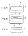
- Figs. 2a-2c are cross sectional views showing successive steps in producing an epitaxial growth substrate according to the present invention.
- a sapphire substrate 11 as a base material is set into a nitriding vessel 12 having an high temperature ammonia atmosphere of 1000°C therein, and is exposed to the high temperature ammonia atmosphere to form an aluminum nitride film 13 on the C-face of the sapphire substrate.
- the aluminum nitride film have its small thickness of for example, 100 ⁇ .
- the nitriding vessel 12 can be common to the CVD chamber 14.
- the Al x Ga y In z N film 15 is formed, by epitaxial growth, on the aluminum nitride film 13 which is formed by nitriding the C-face of the sapphire substrate 11, it can have its excellent crystallinity through a small amount of defect, but can not have its excellent surface flatness. Therefore, if an additional Al x Ga y In z N film is epitaxially grown on the Al x Ga y In z N film 15, it can not have its excellent characteristics due to the rough surface flatness. As a result, the epitaxial growth substrate composed of the sapphire substrate 11 and the Al x Ga y In z N film 15 can not be practically used.
- the surface part of the Al x Ga y In z N film 15 is polished by chemical mechanical polishing, so that the Al x Ga y In z N film 15 is flattened.
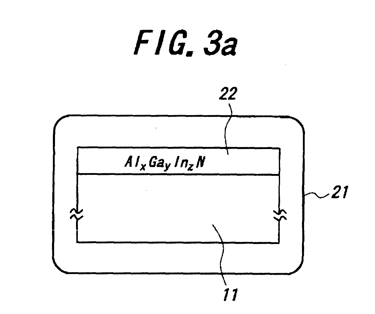
- Figs. 3a and 3b are cross sectional views showing successive steps in producing another epitaxial growth substrate according to the present invention.
- the sapphire substrate 11 as a base material is set into a CVD chamber 21, and an Al x Ga y In z N film 22 is epitaxially grown in a thickness of 1.1 ⁇ m on the C-face of the substrate by high temperature CVD under a temperature of 1000°C or over.
- the Al x Ga y In z N film 22 can have its excellent crystallinity through a small amount of defect by the epitaxial growth at the high temperature.
- the sapphire substrate 11 having the Al x Ga y In z N film 22 thereon is taken out of the CVD chamber 21, and as shown in Fig. 3b, the surface part of the Al x Ga y In z film 22 is polished in a thickness of about 1.0 ⁇ m by chemical mechanical polishing. If an additional Al x Ga y In z N film is formed on the Al x Ga y In z N film 22 by epitaxial growth, it can have its excellent crystallinity and surface flatness.
- Figs. 4a-4d are cross sectional views showing successive steps in producing a light emitting diode using the above epitaxial growth substrate.
- an epitaxial growth substrate 31 has the sapphire substrate 11, the aluminum nitride film 13 with a thickness of 100 ⁇ formed by nitriding the surface of the sapphire substrate 11, and the Al x Ga y In z N film 15 with a thickness of 1 ⁇ m formed by epitaxial growth on the aluminum nitride film 13.
- the Al x Ga y In z N film 15 with a thickness of 1 ⁇ m formed by epitaxial growth on the aluminum nitride film 13.
- the n-type Al x Ga y In z N film 33 can have its excellent crystallinity and surface flatness.
- the p-type Al x Ga y In z N film can have its excellent crystallinity and surface flatness due to the crystallinity and surface flatness of the Al x Ga y In z N film 15.
- the p-type Al x Ga y In z N films 34 and 35 are partially etched and removed to expose a part of the surface of the n-type Al x Ga y In z N film 33.
- an electrode 36 is formed on the exposed part of the surface of the n-type Al x Ga y In z N film 33 and an electrode 37 is formed on the low resistive p-type Al x Ga y In z N film 35.
- Figs. 5a-5c are cross sectional views showing successive steps in producing a light emitting diode using another epitaxial growth substrate according to the present invention.
- the above epitaxial growth substrate may be composed of a SiC substrate or a GaN substrate as a base material instead of the sapphire substrate.
- another electronic device such as a light emitting diode to emit another color light or ultraviolet light, a laser diode and a field effect transistor can be produced.
- the epitaxially grown Al x Ga y In z N film on the sapphire substrate is polished by chemical mechanical polishing, but it may done by mechanical polishing or the combination of chemical mechanical polishing and mechanical polishing.
- the epitaxial growth substrate of the present invention has an Al x Ga y In z N film with its excellent crystallinity and surface flatness thereon which is epitaxially grown on a base material such as a sapphire substrate directly or via a nitride film formed by nitriding the surface of the base material and is polished. Therefore, an additional Al x Ga y In z N film formed by epitaxial growth on the epitaxial growth substrate can have its excellent crystallinity and surface flatness due to the crystallinity and surface flatness of the Al x Ga y In z N film of the epitaxial growth substrate. As a result, if a light emission element is made by using the epitaxial growth substrate, it can have a high light emission efficiency.
- the Al x Ga y In z N film formed on the base material directly or via the nitride film formed by nitriding the surface of the base material can have a large thickness at a high temperature by CVD, it can have its excellent crystallinity.
- the Al x Ga y In z N film can have its surface flatness through polishing.
Landscapes
- Chemical & Material Sciences (AREA)
- Engineering & Computer Science (AREA)
- Crystallography & Structural Chemistry (AREA)
- Materials Engineering (AREA)
- Metallurgy (AREA)
- Organic Chemistry (AREA)
- Chemical Kinetics & Catalysis (AREA)
- General Chemical & Material Sciences (AREA)
- Inorganic Chemistry (AREA)
- Led Devices (AREA)
- Recrystallisation Techniques (AREA)
- Crystals, And After-Treatments Of Crystals (AREA)
Abstract
Description
Accordingly, when an additional AlxGayInzN (x+y+z=1,x,y,z≥0) film is formed on the epitaxial growth substrate by epitaxially growth, it can have its excellent crystallinity and surface flatness.
Therefore, in this case, it is preferable to form a high crystallinity nitride film between the base material and the AlxGayInzN film, in view of the above enhancement for the crystallinity and surface flatness of the additional AlxGayInzN film.
Claims (15)
- An epitaxial growth substrate comprising a base material and an AlxGayInzN (x+y+z=1,x,y,z≥0) film, on one surface of the base material, of which the opposite surface to the base material is polished and thus, flattened.
- An epitaxial growth substrate as defined in claim 1, wherein the AlxGayInzN film has a surface roughness Ra of less than 10Å.
- An epitaxial growth substrate as defined in claim 1 or 2, wherein the AlxGayInzN film has a thickness of about 1.0 µm.
- An epitaxial growth substrate as defined in any one of claims 1-3, further comprising a high crystallinity nitride film between the base material and the AlxGayInzN film.
- An epitaxial growth substrate as defined in any one of claims 1-4, wherein the base material is composed of a sapphire substrate.
- An epitaxial growth substrate as defined in claim 5, wherein the high crystallinity nitride film is an aluminum nitride film.
- A method for producing an epitaxial growth substrate comprising the steps of:preparing a base material,epitaxially growing an AlxGayInzN (x+y+z=1,x,y,z≥0) film on one surface of the base material, andpolishing and thus, flattening the opposite surface of the AlxGayInzN film to the base material.
- A method for producing an epitaxial growth substrate as defined in claim 7, wherein the polishing of the AlxGayInzN film is carried out by chemical mechanical polishing.
- A method for producing an epitaxial growth substrate as defined in claim 7 or 8, wherein the opposite surface of the AlxGayInzN film is flattened to a surface roughness Ra of less than 10Å.
- A method for producing an epitaxial growth substrate as defined in any one of claims 7-9, wherein the AlxGayInzN film is epitaxially grown in a thickness of about 1.1 µm, and is polished up to a thickness of about 1.0 µm.
- A method for producing an epitaxial growth substrate as defined in any one of claims 7-10, further comprising the step of forming a high crystallinity nitride film between the base material and the AlxGayInzN film.
- A method for producing an epitaxial growth substrate as defined in claim 11, wherein the high crystallinity nitride film is made by nitriding the one surface of the base material.
- A method for producing an epitaxial growth substrate as defined in claim 12, wherein the base material is composed of a sapphire substrate.
- A method for producing an epitaxial growth substrate as defined in claim 13, wherein the high crystallinity nitride film is an aluminum nitride film.
- A light emitting diode comprising an epitaxial growth substrate as defined in any one of claims 1-6.
Applications Claiming Priority (2)
| Application Number | Priority Date | Filing Date | Title |
|---|---|---|---|
| JP32656199A JP2001144014A (en) | 1999-11-17 | 1999-11-17 | Substrate for epitaxial growth and method of manufacturing the same |
| JP32656199 | 1999-11-17 |
Publications (2)
| Publication Number | Publication Date |
|---|---|
| EP1101842A2 true EP1101842A2 (en) | 2001-05-23 |
| EP1101842A3 EP1101842A3 (en) | 2005-08-17 |
Family
ID=18189210
Family Applications (1)
| Application Number | Title | Priority Date | Filing Date |
|---|---|---|---|
| EP00124939A Withdrawn EP1101842A3 (en) | 1999-11-17 | 2000-11-15 | Substrate for epitaxy of III-V compounds and a method for producing the same |
Country Status (3)
| Country | Link |
|---|---|
| US (1) | US6554896B1 (en) |
| EP (1) | EP1101842A3 (en) |
| JP (1) | JP2001144014A (en) |
Cited By (3)
| Publication number | Priority date | Publication date | Assignee | Title |
|---|---|---|---|---|
| US7655197B2 (en) | 2000-03-13 | 2010-02-02 | Cree, Inc. | III-V nitride substrate boule and method of making and using the same |
| US7781314B2 (en) | 2003-03-05 | 2010-08-24 | Sumitomo Electric Industries, Ltd. | Nitride semiconductor device manufacturing method |
| EP2124258A3 (en) * | 2008-05-22 | 2011-03-02 | Sharp Kabushiki Kaisha | Mos field effect transistor and manufacturing method for the same |
Families Citing this family (8)
| Publication number | Priority date | Publication date | Assignee | Title |
|---|---|---|---|---|
| US6488767B1 (en) * | 2001-06-08 | 2002-12-03 | Advanced Technology Materials, Inc. | High surface quality GaN wafer and method of fabricating same |
| JP4784012B2 (en) * | 2001-07-27 | 2011-09-28 | 日亜化学工業株式会社 | Nitride semiconductor substrate and manufacturing method thereof |
| JP4514727B2 (en) * | 2001-12-25 | 2010-07-28 | 日本碍子株式会社 | Group III nitride film manufacturing method, group III nitride film, group III nitride element epitaxial substrate, and group III nitride element |
| JP2003327497A (en) * | 2002-05-13 | 2003-11-19 | Sumitomo Electric Ind Ltd | GaN single crystal substrate, nitride-based semiconductor epitaxial substrate, nitride-based semiconductor device, and method of manufacturing the same |
| TW561637B (en) * | 2002-10-16 | 2003-11-11 | Epistar Corp | LED having contact layer with dual dopant state |
| JP2006206343A (en) * | 2005-01-25 | 2006-08-10 | Ngk Insulators Ltd | Surface flattening method of AlN single crystal and manufacturing method of AlN single crystal substrate |
| KR100766858B1 (en) * | 2006-03-16 | 2007-10-12 | 서울옵토디바이스주식회사 | Buffer layer forming method for nitride semiconductor light emitting device and nitride semiconductor light emitting device thereof |
| JP2011222969A (en) * | 2010-03-26 | 2011-11-04 | Ngk Insulators Ltd | Method of manufacturing epitaxial substrate for semiconductor device, epitaxial substrate for semiconductor device, and semiconductor device |
Family Cites Families (7)
| Publication number | Priority date | Publication date | Assignee | Title |
|---|---|---|---|---|
| JPH0754806B2 (en) * | 1987-01-20 | 1995-06-07 | 日本電信電話株式会社 | Method for growing compound semiconductor single crystal film |
| US6020602A (en) * | 1996-09-10 | 2000-02-01 | Kabushiki Kaisha Toshba | GaN based optoelectronic device and method for manufacturing the same |
| JP3361964B2 (en) * | 1996-09-10 | 2003-01-07 | 株式会社東芝 | Semiconductor light emitting device and method of manufacturing the same |
| PL184902B1 (en) * | 1997-04-04 | 2003-01-31 | Centrum Badan Wysokocisnieniowych Pan | Method of removing roughness and strongly defective areas from surface of gan and ga1-x-y-alxinyn crystals and epitaxial layers |
| JP3395631B2 (en) * | 1997-04-17 | 2003-04-14 | 日亜化学工業株式会社 | Nitride semiconductor device and method of manufacturing nitride semiconductor device |
| JPH11261106A (en) * | 1998-03-12 | 1999-09-24 | Nippon Telegr & Teleph Corp <Ntt> | Semiconductor device |
| JP3201475B2 (en) * | 1998-09-14 | 2001-08-20 | 松下電器産業株式会社 | Semiconductor device and method of manufacturing the same |
-
1999
- 1999-11-17 JP JP32656199A patent/JP2001144014A/en active Pending
-
2000
- 2000-11-15 EP EP00124939A patent/EP1101842A3/en not_active Withdrawn
- 2000-11-15 US US09/713,636 patent/US6554896B1/en not_active Expired - Lifetime
Cited By (5)
| Publication number | Priority date | Publication date | Assignee | Title |
|---|---|---|---|---|
| US7655197B2 (en) | 2000-03-13 | 2010-02-02 | Cree, Inc. | III-V nitride substrate boule and method of making and using the same |
| US7915152B2 (en) | 2000-03-13 | 2011-03-29 | Cree, Inc. | III-V nitride substrate boule and method of making and using the same |
| US8212259B2 (en) | 2000-03-13 | 2012-07-03 | Cree, Inc. | III-V nitride homoepitaxial material of improved quality formed on free-standing (Al,In,Ga)N substrates |
| US7781314B2 (en) | 2003-03-05 | 2010-08-24 | Sumitomo Electric Industries, Ltd. | Nitride semiconductor device manufacturing method |
| EP2124258A3 (en) * | 2008-05-22 | 2011-03-02 | Sharp Kabushiki Kaisha | Mos field effect transistor and manufacturing method for the same |
Also Published As
| Publication number | Publication date |
|---|---|
| JP2001144014A (en) | 2001-05-25 |
| EP1101842A3 (en) | 2005-08-17 |
| US6554896B1 (en) | 2003-04-29 |
Similar Documents
| Publication | Publication Date | Title |
|---|---|---|
| US6426519B1 (en) | Epitaxial growth substrate and a method for producing the same | |
| US6110277A (en) | Process for the fabrication of epitaxial layers of a compound semiconductor on monocrystal silicon and light-emitting diode fabricated therefrom | |
| US7180088B2 (en) | Nitride based semiconductor light-emitting device | |
| US20080191191A1 (en) | Light Emitting Diode of a Nanorod Array Structure Having a Nitride-Based Multi Quantum Well | |
| EP1605522A1 (en) | Semiconductor light-emitting element and method for manufacturing same; integrated semiconductor light-emitting device and method for manufacturing same; image display and method for manufacturing same; and illuminating device and method for manufacturing same | |
| CN101258616A (en) | Semiconductor light emitting device and lighting apparatus using the same | |
| KR20050084774A (en) | Gallium nitride-based devices and manufacturing process | |
| JP6472459B2 (en) | Optoelectronic semiconductor chip manufacturing method and optoelectronic semiconductor chip | |
| TW201005828A (en) | Method of forming a semiconductor structure | |
| CN102959739A (en) | Group III nitride semiconductor device and method for producing same | |
| JP7407303B2 (en) | LED precursor | |
| US6554896B1 (en) | Epitaxial growth substrate and a method for producing the same | |
| KR100682873B1 (en) | Semiconductor light emitting device and method for manufacturing same | |
| CN114503290B (en) | LED precursors containing strain relaxation structures | |
| KR100616543B1 (en) | Nitride single crystal growth method on silicon substrate, nitride semiconductor light emitting device using same and manufacturing method thereof | |
| JP3289682B2 (en) | Semiconductor light emitting device | |
| US11616164B2 (en) | Method for producing a nitride compound semiconductor component | |
| JP2000114599A (en) | Semiconductor light emitting device | |
| US20060289891A1 (en) | Electronic and/or optoelectronic devices grown on free-standing GaN substrates with GaN spacer structures | |
| JP3541775B2 (en) | Group III nitride semiconductor light emitting device wafer, method of manufacturing the same, and group III nitride semiconductor light emitting device | |
| JPH05243613A (en) | Light emitting device and manufacturing method thereof | |
| JP7338045B2 (en) | Light Emitting Diode and Method of Forming Light Emitting Diode | |
| JPH09237938A (en) | III-V group compound semiconductor device | |
| JP2000012979A (en) | Method for manufacturing nitride semiconductor substrate | |
| JP2000332293A (en) | III-V nitride semiconductor light emitting device and method of manufacturing the same |
Legal Events
| Date | Code | Title | Description |
|---|---|---|---|
| PUAI | Public reference made under article 153(3) epc to a published international application that has entered the european phase |
Free format text: ORIGINAL CODE: 0009012 |
|
| AK | Designated contracting states |
Kind code of ref document: A2 Designated state(s): AT BE CH CY DE DK ES FI FR GB GR IE IT LI LU MC NL PT SE TR |
|
| AX | Request for extension of the european patent |
Free format text: AL;LT;LV;MK;RO;SI |
|
| PUAL | Search report despatched |
Free format text: ORIGINAL CODE: 0009013 |
|
| AK | Designated contracting states |
Kind code of ref document: A3 Designated state(s): AT BE CH CY DE DK ES FI FR GB GR IE IT LI LU MC NL PT SE TR |
|
| AX | Request for extension of the european patent |
Extension state: AL LT LV MK RO SI |
|
| RIC1 | Information provided on ipc code assigned before grant |
Ipc: 7C 30B 29/40 B Ipc: 7C 30B 25/18 B Ipc: 7H 01L 21/20 B Ipc: 7H 01L 33/00 B Ipc: 7H 01L 21/306 A |
|
| STAA | Information on the status of an ep patent application or granted ep patent |
Free format text: STATUS: THE APPLICATION IS DEEMED TO BE WITHDRAWN |
|
| 18D | Application deemed to be withdrawn |
Effective date: 20050601 |