EP1098428B1 - Semiconductor power converting apparatus - Google Patents
Semiconductor power converting apparatus Download PDFInfo
- Publication number
- EP1098428B1 EP1098428B1 EP00117732A EP00117732A EP1098428B1 EP 1098428 B1 EP1098428 B1 EP 1098428B1 EP 00117732 A EP00117732 A EP 00117732A EP 00117732 A EP00117732 A EP 00117732A EP 1098428 B1 EP1098428 B1 EP 1098428B1
- Authority
- EP
- European Patent Office
- Prior art keywords
- voltage
- gate
- collector
- emitter
- semiconductor element
- Prior art date
- Legal status (The legal status is an assumption and is not a legal conclusion. Google has not performed a legal analysis and makes no representation as to the accuracy of the status listed.)
- Expired - Lifetime
Links
- 239000004065 semiconductor Substances 0.000 title claims description 121
- 230000007935 neutral effect Effects 0.000 claims description 5
- 230000000630 rising effect Effects 0.000 claims description 2
- 238000005513 bias potential Methods 0.000 claims 1
- 238000010586 diagram Methods 0.000 description 17
- 239000003990 capacitor Substances 0.000 description 12
- 230000000694 effects Effects 0.000 description 5
- 230000000295 complement effect Effects 0.000 description 4
- 230000001629 suppression Effects 0.000 description 2
- 230000003247 decreasing effect Effects 0.000 description 1
- 230000004048 modification Effects 0.000 description 1
- 238000012986 modification Methods 0.000 description 1
- 230000000087 stabilizing effect Effects 0.000 description 1
Images



Classifications
-
- H—ELECTRICITY
- H02—GENERATION; CONVERSION OR DISTRIBUTION OF ELECTRIC POWER
- H02M—APPARATUS FOR CONVERSION BETWEEN AC AND AC, BETWEEN AC AND DC, OR BETWEEN DC AND DC, AND FOR USE WITH MAINS OR SIMILAR POWER SUPPLY SYSTEMS; CONVERSION OF DC OR AC INPUT POWER INTO SURGE OUTPUT POWER; CONTROL OR REGULATION THEREOF
- H02M1/00—Details of apparatus for conversion
- H02M1/08—Circuits specially adapted for the generation of control voltages for semiconductor devices incorporated in static converters
-
- H—ELECTRICITY
- H03—ELECTRONIC CIRCUITRY
- H03K—PULSE TECHNIQUE
- H03K17/00—Electronic switching or gating, i.e. not by contact-making and –breaking
- H03K17/16—Modifications for eliminating interference voltages or currents
- H03K17/168—Modifications for eliminating interference voltages or currents in composite switches
-
- H—ELECTRICITY
- H03—ELECTRONIC CIRCUITRY
- H03K—PULSE TECHNIQUE
- H03K4/00—Generating pulses having essentially a finite slope or stepped portions
-
- H—ELECTRICITY
- H03—ELECTRONIC CIRCUITRY
- H03K—PULSE TECHNIQUE
- H03K17/00—Electronic switching or gating, i.e. not by contact-making and –breaking
- H03K17/16—Modifications for eliminating interference voltages or currents
- H03K17/161—Modifications for eliminating interference voltages or currents in field-effect transistor switches
- H03K17/165—Modifications for eliminating interference voltages or currents in field-effect transistor switches by feedback from the output circuit to the control circuit
- H03K17/166—Soft switching
Definitions
- the present invention relates to a semiconductor power converting apparatus with employment of a semiconductor element and the like. More specifically, the present invention relates to a semiconductor power converting apparatus capable of suppressing a peak voltage during a switching operation without requiring a snubber circuit.
- IGBTs Insulated-Gate Bipolar Transistor
- a typical insulated-gate transistor own low gate power consumption and can be switched in high speeds with a small switching loss. Accordingly, these IGBTs are employed in semiconductor power converting apparatuses having relatively medium and small capacities. Furthermore, these IGBTs are desirably applied to semiconductor power converting apparatuses having large capacities.
- this jump-up voltage ⁇ V is direct proportional to both a switching current I and a root-mean-squared value of a wiring inductance L. Therefore, in the case that a wiring inductance L can be minimized and a switching current I is low in a semiconductor power converting apparatus having a medium/small capacity, since a switching loss E off of an IGBT is present, this power converting apparatus can be made in a snubberless form, namely a snubber capacitor C is omitted.
- a semiconductor power converting apparatus having a large capacity requires such a snubber circuit for suppressing a peak voltage produced when a large switching current is turned OFF, and furthermore, another snubber circuit for equally sharing a high DC voltage to series-connected semiconductor elements.
- switching losses of these snubber circuits would reduce the converter efficiency, namely could not be neglected.
- the snubber circuits are connected to such a semiconductor power converting apparatus, the cost thereof is increased and this semiconductor power converting apparatus becomes bulky.
- both ON timing and OFF timing of all of these IGBTs must be adjusted in high precision in order to equally sharing the voltages to these IGBTs. This requires time and high cost. As a result, very recently, various circuit systems have been proposed.
- the peak voltages are suppressed when the IGBTs are turned OFF.
- the stational voltage sharing operation for the series-connected IGBTs is uniformly carried out on that any snubber circuit.
- This recently proposed circuit system corresponds to, as described in Japanese patent application No. 9-334633, the gate driving circuit with the basic circuit arrangement such that the zener diode is connected between the collector of the IGBT and the gate thereof, or the series circuit made of the zener diode and the resistor is connected between the collector and the gate of the IGBT.
- the avalanche current will flow when the collector voltage of the IGBT becomes higher than, or equal to the avalanche voltage of the zener diode, and thus, since the voltage of the gate resistor is increased, the peak value of the collector voltage of this IGBT is suppressed.
- an avalanche voltage of a zener diode would also require several Kilovolts.
- avalanche currents having values of several to several tens of Amperes are required.
- a resistance value of a gate resistor would also require approximately several tens of Ohms, so that the switching loss of this IGBT would be increased.
- EP-A-0 730 331 discloses a circuit for limiting switching overvoltages in semiconductor switches as used in semiconductor power converting apparatuses having the features of the precharacterizing portion of claim 1.
- the circuit comprises a control path connected in parallel with a power semiconductor element and containing a resistive voltage divider in series with a capacitor and a diode.
- the voltage divider tap-off point is coupled to the semiconductor gate, so that the latter conducts in response to an overvoltage across the semiconductor element.
- a disadvantage of this circuit is that the gate cannot be actively discharged and in case an overvoltage occurs and the gate conducts again, it takes too much time to switch off the gate. Consequently, the switching frequency is low.
- the present invention has been made to solve the above-explained problems, and therefore, has an object to provide a semiconductor power converting apparatus capable of making an electric power converting apparatus compact and in low cost, and capable of operating the electric power converting apparatus in a high efficiency.
- the semiconductor power converting apparatus comprises: a semiconductor element for controlling a current flowing between a collector and an emitter in response to a gate condition; a driving device connected to the gate, for driving the gate in response to a drive signal entered therinto; a voltage applying device for applying both a forward bias and a reverse bias to the gate so as to set the emitter of the semiconductor element to a neutral potential; and a voltage dividing device for dividing a voltage appearing between the collector and the emitter of the semiconductor element; wherein: when the drive signal is under OFF state, a voltage produced based upon the divided voltage by the voltage dividing device is applied to the gate; and the gate voltage is controlled in response to the voltage appearing between the collector and the emitter of the semiconductor element.
- the semiconductor power converting device is further featured in that the voltage dividing device includes the collector and a minus-polarity terminal for applying the reverse bias voltage.
- the semiconductor power converting apparatus may comprise; a selecting device made by a switching element connected to a gate of a semiconductor element typically known as an insulating gate transistor, capable of selecting a drive signal in response to either an ON command or an OFF command issued by a control device; a voltage source for applying both a forward bias and a reverse bias to the gate while setting the emitter for driving the semiconductor element as a neutral potential; and a voltage dividing device for dividing a voltage appearing between the collector of the semiconductor element and a minus-sided electrode of the voltage source by employing a resistor, in which when the drive signal is an OFF command, a gate voltage of the semiconductor element becomes such a voltage value corresponding to the voltage division; in which when the voltage appearing between the collector of the semiconductor element and the emitter thereof is higher than, or equal to a predetermined voltage, the voltage dividing device can suppress this peak voltage.
- a selecting device made by a switching element connected to a gate of a semiconductor element typically known as an insulating gate transistor, capable of selecting a drive
- the reverse bias voltage can be applied just after the semiconductor element is turned OFF without increasing the gate resistance with being turned OFF.
- the gate voltage is switched from the reverse bias voltage to the forward bias voltage in response to the voltage between the collector and the emitter.
- the voltage between the collector and the emitter of the semiconductor element becomes high, the peak voltage of the voltage between the collector and the emitter is suppressed by utilizing the gate voltage of the forward bias voltage in response to this voltage between the collector and the emitter.
- the semiconductor power converting apparatus may comprise: a selecting device made by a switching element connected to a gate of a semiconductor element, capable of selecting a drive signal in response to either an ON command or an OFF command issued by a control device; a voltage source for applying both a forward bias and a reverse bias to the gate while setting the emitter for driving the semiconductor element as a neutral potential; a voltage dividing device for dividing a voltage appearing between the collector of the semiconductor element and the emitter thereof, or a voltage appearing between the collector of the semiconductor element and a minus-sided electrode of the voltage source by employing a resistor, in which when the drive signal is an OFF command, a gate voltage of the semiconductor element is brought into such a voltage condition corresponding to the voltage division; and a switching device for switching the gate voltage in such a manner that the gate voltage is equal to a negative voltage corresponding to the source voltage of the voltage source when the divided voltage detected by the voltage dividing device is lower than a set voltage, and also the gate voltage is equal to a voltage value produced
- the reverse bias voltage can be applied just after the semiconductor element is turned OFF without increasing the gate resistance when being turned OFF.
- the gate voltage is switched from the reverse bias voltage to the forward bias voltage in response to the voltage between the collector and the emitter.
- the reverse bias voltage is applied to the gate so as to increase the noise margin performance.
- the voltage between the collector and the emitter of the semiconductor element becomes high, the peak voltage of the OFF-voltage between the collector and the emitter is suppressed by applying the gate voltage of the forward bias voltage directly proportion to this voltage between the collector and the emitter.
- the semiconductor power converting device may comprise: a driving device connected to a gate of a semiconductor element, for applying both a forward bias and a reverse bias to the gate of the semiconductor element by employing a first switch and a second switch, the first switch series-connected to a resistor being turned ON in response to an ON command issued by a control device, and the second switch series-connected to a resistor being turned ON in response to an OFF command issued by the control device; a voltage source for applying both a forward bias and a reverse bias to the gate while setting the emitter for driving the semiconductor element as a neutral potential; voltage dividing device for dividing a voltage appearing between the collector of the semiconductor element and the emitter thereof, or a voltage appearing between the collector of the semiconductor element and a minus-sided electrode of the voltage source by employing a resistor, and for detecting a voltage appearing between the collector and the emitter of the semiconductor element; and an adjusting device constituted by a third switch parallel-connected to a first switch, and a fourth switch series-connected to a
- the switching losses produced when the semiconductor element is turned ON and also turned OFF can be reduced.
- this peak voltage can be suppressed.
- the gate voltage is switched from the reverse bias voltage to a bias voltage direct proportional to the forward bias voltage.
- the semiconductor power converting apparatus of the present invention may be featured in that either a zener diode or a voltage source is inserted in series to a voltage dividing resistor which divides a voltage appearing between an emitter and a collector of a semiconductor element so as to increase a changing ratio of a gate voltage with respect to the voltage between the emitter and the collector of this semiconductor element while a peak voltage is suppressed.
- a voltage dividing resistor which divides a voltage appearing between an emitter and a collector of a semiconductor element so as to increase a changing ratio of a gate voltage with respect to the voltage between the emitter and the collector of this semiconductor element while a peak voltage is suppressed.
- the peak voltage suppressing effect is improved.
- the peak voltage suppressing operation when the semiconductor element is turned OFF can be effectively carried out.
- the semiconductor power converting apparatus of the present invention may be featured in that a circuit constituted by either a capacitor or a switch is connected in parallel to a portion of a voltage dividing resistor which divides a voltage appearing between a collector of a semiconductor element and an emitter thereof, and such a device is provided which changes a voltage dividing ratio in such a manner that a relationship between the gate voltage and the collector potential can be continuously, or stepwise changed, and rising of the collector potential is commenced. Then, the voltage dividing device can suppress a peak voltage appearing between the collector and the emitter by changing the setting condition even when dv/dt of the voltage between the collector and the emitter of the semiconductor element is high.
- the semiconductor power converting apparatus of the present invention may be featured by employing a device for changing a voltage dividing ratio by way of a timer switch connected in parallel to a portion of a voltage dividing resistor which divides a voltage appearing between a collector of a semiconductor element and an emitter thereof. Then, after the semiconductor element has been turned OFF, the voltage between the collector and the emitter of the semiconductor element is stationally stabilized with respect to the power supply voltage. After a preselected time period has passed, the voltage dividing ratio is changed into a higher value than the power supply voltage, so that the reverse bias can be applied to the gate of the semiconductor element.
- the semiconductor power converting apparatus of the present invention may be featured in that more than two sets of semiconductor elements are connected in series to each other so as to constitute an arm, the arms are simultaneously turned ON, or OFF. Then, a voltage dividing ratio of a voltage dividing device is set in such a manner that the voltages between the collectors and the emitters of the respective semiconductor elements can be equally shared, so that the voltages between the collectors and the emitters of the series-connected semiconductor elements may be made equal.
- the semiconductor power converting apparatus that a plurality of series-connected semiconductor elements are simultaneously turned ON or OFF, the peak voltage of the voltage appearing between the collector and the emitter of each of the semiconductor elements series-connected to each other can be suppressed. Also, the stationary voltage stabilizing operation after suppressing the peak voltage is carried out in a highspeed, and the switching frequency of the semiconductor power apparatus converting apparatus is increased. As a result, the power converting efficiency can be increased.
- the semiconductor power converting apparatus may comprise: a semiconductor element for controlling a current flowing between a collector and an emitter in response to a gate condition; a driving device connected to the gate, for driving the gate in response to a drive signal; a bias applying device for applying both a forward bias and a reverse bias to the gate; and a voltage dividing device for dividing a voltage appearing between the collector and the emitter of the semiconductor element; wherein: when the drive signal is under OFF state and also a voltage appearing between the collector and the emitter is higher than, or equal to the voltage determined by the voltage dividing means the bias applying means applies a forward bias to the gate.
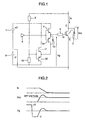
- Fig. 1, Fig. 2 and Fig. 3 are diagram for indicating a first embodiment mode of the present invention.
- Fig. 1 represents an arrangement of a main circuit in unit of an arm.
- a cross-connected diode 2 is connected to an insulated-gate transistor 1, and both a transistor 4 and another transistor 5a are connected to a gate resistor 3.
- both an ON command and an OFF command are supplied from a control circuit 6 to these transistors 4 and 5a.
- a power supply 7 and another power supply 8 are provided so as to set bias voltages.
- a collector electrode C of the insulated-gate transistor 1 and a minus-polarity terminal of the power supply 8 a series member constituted by a resistor 9 and a resistor 10 is connected.
- the transistor 11 and the transistor 12 are connected in a complementary connection manner.
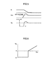
- FIG. 2 graphically shows a collector current Ic when the insulated-gate transistor 1 is turned OFF, a voltage V CE between the collector and the emitter of the insulated-gate transistor 1, and also a gate voltage Vg indicated in Fig. 1.
- the ON signal is outputted from the control circuit 6, the transistor 4 of the power supply 7 is applied to the gate terminal of the insulated-gate transistor 1 via the gate resistor 3, so that this insulated-gate transistor 1 is brought into an ON state.
- This reverse bias voltage may extract gate charges between the gate and the emitter of the insulated-gate transistor 1.
- the voltage V CE of the insulated-gate transistor 1 whose gate charges have been extracted starts to be increased.
- the voltage at the gate electrode is similarly increased in response to such a voltage obtained by dividing the voltage V CE by the resistors 9 and 10. Since this voltage dividing ratio of the resistor 9 and the resistor 10 is determined in such a manner that the gate voltage Vg is approximated to 0 V at a preset value of the voltage V CE , when this voltage V CE is higher than the set voltage, a forward bias voltage corresponding to this voltage V CE is applied to the gate electrode, so that an impedance between the collector and emitter of the insulated-gate transistor 1 may be decreased. As a result, a peak voltage of the voltage V CE may be suppressed. When the peak voltage of the voltage V CE is converged to a voltage near the set voltage, this voltage Vg is also converged to a voltage near zero V.
- Fig. 3 graphically shows a relationship between V CE and Vg.
- a position on an abscissa where Vg becomes 0 and is intersected with V CE corresponds to a set voltage of V CE .
- the gate voltage "Vg" is substantially direct proportion to the voltage "V CE ".
- the peak voltage can be suppressed based upon the gate voltage Vg corresponding to the voltage V CE .
- the voltage utilization efficiency of the semiconductor element can be increased.
- such a compact semiconductor power converting apparatus can be operated in a high efficiency, while no longer the snubber circuit is required, or the snubber circuit can be operated under low capacity.
- Fig. 4 and Fig. 5 indicate a second embodiment mode of the present invention.
- Fig. 4 represents an arrangement of a major circuit in unit of an arm.
- a voltage detected by a detecting circuit having a similar circuit arrangement to that of the above-explained first embodiment mode is compared with a reference voltage decided by a resistor 13 and a resistor 14 in a comparator 15.
- the detecting circuit divides a voltage appearing between a collector of an insulated-gate transistor 1 and a minus-polarity terminal of a power supply 8.
- the comparator 15 causes a transistor 16 to be turned OFF and another transistor 17 to be turned ON, so that this detected voltage becomes a reverse bias voltage corresponding to a power supply voltage "Vge" of the power supply 8.
- the comparator 15 when the detected voltage is higher than, or equal to the reference voltage, the comparator 15 outputs such a voltage responding to the detected voltage, and both the transistor 16 and the transistor 17 which are connected in a complementary manner will output a similar voltage.
- the gate voltage Vg when the reference voltage is made substantially equal to the set voltage of the voltage V CE , the gate voltage Vg can be applied as a forward voltage corresponding to the voltage V CE only when the voltage V CE becomes higher than the set voltage.
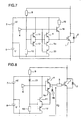
- FIG. 5 graphically shows a collector current Ic when the insulated-gate transistor 1 is turned OFF, a voltage V CE between the collector and the emitter of the insulated-gate transistor 1, and also a gate voltage Vg indicated in Fig. 4.
- the transistor 4 of the power supply 7 is applied to the gate terminal of the insulated-gate transistor 1 via the gate resistor 3, so that this insulated-gate transistor 1 is brought into an ON state.
- the voltage V CE of the insulated-gate transistor 1 is substantially equal to 0 V
- the voltage outputted from the complementary-connected transistors 11 and 12 becomes substantially equal to the voltage appearing on the minus-polarity terminal of the power supply 8.
- the control circuit 6 outputs the OFF signal
- the transistor 4 is turned OFF and the transistor 5a is turned ON.
- the comparator 15 causes the transistor 17 to be turned ON, so that the gate voltage Vg is set as a reverse bias voltage equivalent to the voltage appearing on the minus-polarity terminal of the power supply 8.
- the gate charges appearing between the gate and the emitter of the insulated-gate transistor 1 are extracted by this reverse bias voltage.
- the voltage V CE of the insulated-gate transistor 1 whose gate electrodes have been extracted starts to be increased. While this voltage V CE is increased, the divided voltage by the resistor 9 and the resistor 10 is also increased. Under such a condition that the divided voltage is lower than the reference voltage produced by the resistor 13 and the resistor 14, the gate voltage Vg becomes such a reverse.bias voltage corresponding to the power supply voltage of the power supply 8.
- the gate voltage Vg is set as a forward bias voltage in response to the voltage V CE by the comparator 15, and the insulated-gate transistor 1 causes the impedance changing ratio between the collector and the emitter to be lowered.
- the peak voltage of the voltage V CE is suppressed.
- this gate voltage Vg is also converged to a voltage near zero V.
- Fig. 7 graphically shows a relationship between V CE and Vg.
- this gate voltage Vg becomes a reverse bias voltage substantially equal to the power supply voltage of the power supply 8.
- this gate voltage Vg is switched to higher than 0 V.
- the gate voltage Vg becomes such a voltage which is substantially direct proportion to the set voltage.
- the peak voltage can be suppressed based upon the gate voltage Vg corresponding to the voltage V CE . In connection thereto, the voltage utilization efficiency of the semiconductor element can be increased.
- the noise margin can be increased in order that the erroneous operations caused by the noise such as the error ignition do not occur. Furthermore, such a compact semiconductor power converting apparatus can be operated in a high efficiency, while no longer the snubber circuit is required, or the snubber circuit can be operated under low capacity.
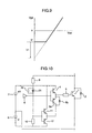
- Fig. 7 represents a third embodiment mode of the present invention.
- Fig. 7 shows an arrangement of the major circuit in unit of an arm.
- a voltage detected by a detecting circuit having a similar circuit arrangement to that of the above-explained first embodiment mode is used to drive both a transistor 4 and a transistor 5a, which are connected in a complementary connection manner.
- This detecting circuit divides a voltage appearing between a collector of an insulated-gate transistor 1 and a minus-polarity electrode of a power supply 8.
- a series member constituted by a transistor 18 and a resistor 19 is connected in parallel to the transistor 4, and is driven by a control circuit 6.
- another transistor 20 driven by the control circuit 6 is connected in series to the transistor 5a.
- both the transistor 4 and the transistor 18 establish a relationship of an OR logic gate circuit.
- the transistor 4 adjusts the gate voltage in response to the divided voltage.
- the transistor 18 is driven by the control circuit 6.
- both the transistor 5a and a transistor 20 establish a relationship of an AND logic gate circuit.
- the transistor 4 adjusts the gate voltage Vg in response to the divided voltage.
- the transistor 20 is driven by the control circuit 6.
- the transistor 4 when the gate voltage Vg responding to the voltage V CE is outputted, the transistor 4 is directly connected to the gate of the insulated-gate transistor 1, so that the voltage V CE with respect to a change in the gate voltages Vg can be quickly controlled.
- the transistor for outputting the gate voltage in response to the voltage V CE and another transistor for normally turning ON the transistor is provided, it is possible to emphasize the suppression effect with respect to the peak voltage caused by the gate voltage Vg in response to the voltage V CE in such a case that this voltage V CE of the insulated-gate transistor 1 is higher than, or equal to the set voltage.
- the voltage utilization efficiency of the semiconductor element can be increased.
- such a compact semiconductor power converting apparatus can be operated in a high efficiency, while no longer the snubber circuit is required, or the snubber circuit can be operated under low capacity.
- Fig. 8 and Fig. 9 indicate a fourth embodiment mode of the present invention.
- Fig. 8 represents an arrangement of a major circuit in unit of an arm.
- a peak voltage of an insulated-gate transistor 1 is suppressed by employing a similar circuit arrangement to that of the above-explained first embodiment mode, namely the gate voltage Vg is controlled by an output voltage from transistors 11 and 12 connected in a complementary manner.
- the gate voltage Vg is controlled by an output voltage from transistors 11 and 12 connected in a complementary manner.
- a zener diode 21 is connected in series to a resistor 9, a changing ratio of the gate voltage Vg in the vicinity of the set voltage of V CE is increased.
- V1 an avalanche voltage of the zener diode 21
- V2 a voltage source
- Fig. 9 graphically shows a relationship between V CE and Vg.
- a position on an abscissa where Vg becomes 0 and is intersected with V CE corresponds to a set voltage of V CE .
- This is equivalent to such a fact that the power supply voltage of the power supply 8 is increased by V1 by way of the zener diode, so that the changing ratio of the gate voltage Vg in the vicinity of the V CE set voltage is increased.
- the converging speed to the set voltage can be increased, the switching frequency can be increased. Furthermore, such a compact semiconductor power converting apparatus can be operated in a high efficiency, while no longer the snubber circuit is required, or the snubber circuit can be operated under low capacity.
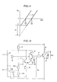
- Fig. 10 and Fig. 11 indicate a fifth embodiment mode of the present invention.
- Fig. 10 represents an arrangement of a major circuit in unit of an arm.
- a capacitor 22 is connected in parallel to this zener diode 21 by employing a similar circuit arrangement to that of the above-explained fourth embodiment mode, namely the resistor 9 is connected in series to the zener diode 21. Since the capacitor 22 is connected to this zener diode, when the voltage V CE after the IGBT is turned OFF rises up, the zener diode 21 cannot be quickly reached to the avalanche voltage due to charging operation of the capacitor 22.
- the gate voltage Vg is set as a forward bias voltage. Since the capacitor 22 is gradually charged, the relationship between V CE and Vg is varied. At such a time instant when the capacitor 22 is charged up to the avalanche voltage of the zener diode 21, the voltage V CE becomes a predetermined set value and becomes stable. Since the capacitance of the capacitor 22 is selected to a proper capacitance value, the effect for suppressing the peak voltage can be improved.
- Fig. 11 graphically shows a relationship between V CE and Vg.
- a position on an abscissa where Vg becomes 0 and is intersected with V CE corresponds to a set voltage of V CE .
- V CE starts to rise up
- no charge is stored in the capacitor 22, and the voltage of the zener diode is equal to 0 V.
- the original V CE set voltage is equivalent to such a voltage condition that this set voltage is lower than, or equal to a predetermined voltage V CE .
- the capacitor 22 is gradually charged up to the voltage of the zener diode 21.
- the set voltage of V CE is gradually increased, and then is reached up to a preselected original set voltage.
- the impedance of the insulated-gate transistor 1 since there are small amounts of a delay defined after the voltage V CE is detected and until the gate voltage Vg is controlled, and another delay with respect to the gate voltage Vg, if the set voltage when the voltage V CE rises up is suppressed to a lower voltage, then the peak suppressing effect can be improved.
- the peak voltage suppressing effect can be emphasized by the gate voltage Vg in accordance with the voltage V CE in such a case that the voltage V CE of the insulated-gate transistor 1 is higher than, or equal to the set voltage in such a form that both the delay in the circuit operation and the response delay of the insulated-gate transistor 1 with respect to the gate voltage Vg can be compensated.
- a compact semiconductor power converting apparatus can be operated in a high efficiency, while no longer the snubber circuit is required, or the snubber circuit can be operated under low capacity.
- Fig. 12, Fig. 13 and Fig. 14 are diagram for indicating a sixth embodiment mode of the present invention.
- Fig. 12 represents an arrangement of a main circuit in unit of an arm. Similar to the circuit arrangement of the first embodiment mode, a resistor 10 used to divide a voltage appearing between a collector of an insulated-gate transistor 1 and a minus-polarity terminal of a power supply 8 is subdivided into a resistor 10a and another resistor 10b. A switch 23 is connected in parallel to the resistor 10b. The switch 23 is brought into an OFF state immediately after the insulated-gate transistor 1 is turned OFF, and a V CE set voltage set by the resistor 9 and the resistors 10a and 10b is brought into a predetermined condition.
- the switch 23 After a peak voltage by turning OFF the insulated-gate transistor 1 is converged up to the power supply voltage, the switch 23 is turned ON, so that the resistor 10b is shortcircuited. As a result, the set voltage with respect to the voltage V CE is changed into a higher set voltage. Since the V CE set voltage is set to such a higher set voltage, the gate voltage Vg becomes a reverse bias voltage of several V, so that the noise margin with respect to the erroneous ignition operation can be increased.
- Fig. 13 graphically shows a relationship between V CE and Vg.
- the relationship between V CE and Vg is a relationship (1) of Fig. 13, and the peak voltage is converged to a set voltage corresponding to the power supply voltage.
- the switch 23 is turned ON.
- the relationship between V CE and Vg may be changed into another relationship (2) of Fig. 13.
- Fig. 14 indicates such a condition that after the voltage V CE has been converged to the set voltage, the switch 23 is turned ON and therefore, a reverse bias voltage of several V is applied.
- the noise margin can be increased in order that the erroneous ignition operations do not occur without employing a complex circuit.
- such a compact semiconductor power converting apparatus can be operated in a high efficiency, while no longer the snubber circuit is required, or the snubber circuit can be operated under low capacity.
- Fig. 15 represents a seventh embodiment mode of the present invention.
- Fig. 15 shows a circuit arrangement of a main circuit in unit of an arm, in which "n" pieces of insulated-gate transistors are series-connected to each other, and are turned ON, or OFF at the same time.
- these insulated-gate transistors 11 to 1n constitute a similar arrangement to that of the first embodiment mode, which divides a voltage appearing between collectors thereof and minus-polarity terminals of power supplies 81 to 8n.
- Each of these insulated-gate transistors 11 to 1n which are simultaneously turned OFF by control circuits 61 to 6n may suppress a peak voltage in a similar manner to that of the first embodiment mode.
- each of these insulated-gate transistors is converged from the peak voltage to a set voltage V CE , the set value of the voltage V CE is made equal to such a voltage produced by equally sharing a DC power supply voltage by "n" pieces of series-connected transistors.
- the power supply voltage can be equally divided.
- the respective insulated-gate transistors which are series-connected to each other own different ground capacitances from each other, and further own different circuit characteristics and different element characteristics from each other. Therefore, a snubber circuit for equally dividing voltages, and also a gate timing controller are required.
- each of these insulated-gate transistors can suppress the peak voltage, and also the power supply voltage can be equally shared by these insulated-gate transistors by converging the voltage to a predetermined voltage V CE .
- the voltage utilization ratio of the semiconductor elements can be increased.
- the snubber circuit is no longer required, or can be operated with a low capacity. Therefore, such a compact semiconductor power converting apparatus operable in a high efficiency can be provided without requiring the selections of the circuits/elements, and the fine adjustment.
- the circuit for constituting the arm is constituted similar to that of the first embodiment mode.
- the circuit arrangements of the above-explained embodiment modes other than this first embodiment mode may be applied to the circuit for constituting the arm.
- the peak voltage can be suppressed.
- the voltage utilization efficiency of the semiconductor element can be increased.
- the snubber circuit is omitted, the snubber loss can be reduced. Therefore, the electric power converting apparatus can be made compact and operable in a high efficiency. Also, the semiconductor power converting apparatus can be made in low cost.
- the suppression effect of the peak voltage can be improved.
- the voltage utilization ratio of the semiconductor element can be increased.
- the converging speed to the set voltage can be shortened, it is possible to provide such a semiconductor power converting apparatus whose switching frequency is set to the high switching frequency.
Landscapes
- Engineering & Computer Science (AREA)
- Power Engineering (AREA)
- Power Conversion In General (AREA)
Description
Claims (11)
- A semiconductor power converting apparatus comprising:characterised bya semiconductor element (1) for controlling a current (IC) flowing between a collector (C) and an emitter (E) in response to a gate (G) voltage (Vg);driving means (6) connected to said gate (G), for driving said gate (G) in response to a drive signal entered thereinto;voltage dividing means (9, 10) for dividing a voltage (VCE) appearing between the collector (C) and the emitter (E) of said semiconductor element (1); andgate voltage control means (11, 12) for controlling the gate voltage (Vg) in response to the voltage (VCE) appearing between the collector (C) and emitter (E) of said semiconductor element (1), by applying a voltage based on the voltage divided by said voltage dividing means (9, 10) to the gate (G) in an OFF-state of the drive signal,
voltage applying means (7, 8) for applying, a forward bias or a reverse bias to said gate (G) while the emitter (E) of said semiconductor element (1) is set to neutral potential; and
switching means (4, 5a, 11, 12)
for applying said reverse bias to said gate (G) when the voltage divided by said voltage dividing means (9, 10) is lower than a set voltage, and
for applying said forward bias to said gate (G) when said voltage divided by said voltage dividing means is higher than the set voltage. - The apparatus of claim 1, further comprising:wherein when the voltage appearing between the collector (C) of said semiconductor element (1) and the emitter (E) thereof is higher than, or equal to a predetermined voltage, said gate voltage is controlled in response to the voltage appearing between the collector (C) and the emitter (E) of said semiconductor element (1).a first switch (4) for adjusting said forward bias based upon the voltage value from said voltage dividing means;a second switch (18) connected in parallel to said first switch (4) and controlled in response to said drive signal;a third switch (5a) for adjusting said reverse bias in response to the voltage value from said voltage dividing means; anda fourth switch (20) connected in series to said third switch (5a) and controlled in response to said drive signal,
- The apparatus of any preceding claim, wherein said voltage dividing means (9, 10) divides a voltage between the collector (C) of said semiconductor element (1) and a minus-side electrode of said voltage applying means by way of a resistor circuit containing a zener diode (21).
- The apparatus of any preceding claim, wherein said voltage dividing means changes a voltage dividing ratio in such a manner that the gate voltage is changed with respect to a collector potential.
- The apparatus of claim 4, wherein said voltage dividing means changes the voltage dividing ratio for a predetermined time period after said drive signal has been switched from the ON state to the OFF state.
- The apparatus of claim 1, wherein
said voltage dividing means is provided for dividing a voltage appearing between a power source line and the collector (C), wherein a voltage is present between the emitter potential of said semiconductor element (1) and the reverse bias potential, and in an OFF-state of the drive signal, the gate voltage of said semiconductor element (1) is made to correspond to the divided voltage,
the gate voltage is controlled in response to and by means of the voltage between the collector (C) and the emitter (E) of said semiconductor element (1), and
when the voltage appearing between the collector (C) of said semiconductor element (1) and the emitter (E) thereof is higher than, or equal to a predetermined voltage, said voltage dividing means controls the gate voltage in response to the voltage appearing between the collector (C) and the emitter (E). - The apparatus of claim 2, wherein said voltage dividing means suppresses a peak voltage appearing between the collector (C) and the emitter (E) by means of the gate voltage and in response to said voltage between the collector (C) and the emitter (E).
- The apparatus of claim 6 or 7, wherein
said voltage dividing means employs either a zener diode (21) or a voltage source to control a voltage changing ratio of the gate (G) signal to the collector (C) potential of the semiconductor element (1), and
said voltage dividing means can suppress a peak voltage appearing between the collector (C) and the emitter (E) based upon a gate voltage and in response to the voltage between the collector (C) and the emitter (E) when the voltage between the collector (C) and the emitter (E) of said semiconductor element (1) is higher than, or equal to a predetermined voltage. - The apparatus of any one of claims 6 to 8, wherein
said voltage dividing means changes a voltage dividing ratio in such a manner that a relationship between the gate voltage and the collector (C) potential can be continuously, or stepwise changed, and rising of the collector (C) potential is commenced, and
said voltage dividing means can suppress a peak voltage appearing between the collector (C) and the emitter (E) based upon a gate voltage and in response to the voltage between the collector (C) and the emitter (E) when the voltage between the collector (C) and the emitter (E) of said semiconductor element (1) is higher than, or equal to a predetermined voltage. - The apparatus of any one of claims 6 to 9, wherein said voltage dividing means reverse-biases a gate (G) signal by timer means for changing the voltage dividing ratio for a predetermined time period after the drive signal is switched ON to OFF.
- The apparatus of any preceding claim, wherein:more than 2 sets of said semiconductor elements (11, ... , 1n) are connected in series to each other so as to constitute an arm,said voltage dividing means owned by each of said semiconductor elements sets the voltage dividing ratio in accordance with a voltage value obtained by dividing a voltage applied to the arm by a total number of said series-connected semiconductor elements of the arm, andwhen a voltage appearing between the collector (C) and the emitter (E) of each of said semiconductor elements is higher than, or equal to a predetermined voltage, the gate voltage of each of said semiconductor element (1) is made a voltage state corresponding to the divided voltage.
Applications Claiming Priority (2)
| Application Number | Priority Date | Filing Date | Title |
|---|---|---|---|
| JP31473499A JP3770008B2 (en) | 1999-11-05 | 1999-11-05 | Semiconductor power converter |
| JP31473499 | 1999-11-05 |
Publications (3)
| Publication Number | Publication Date |
|---|---|
| EP1098428A2 EP1098428A2 (en) | 2001-05-09 |
| EP1098428A3 EP1098428A3 (en) | 2002-01-02 |
| EP1098428B1 true EP1098428B1 (en) | 2004-10-20 |
Family
ID=18056945
Family Applications (1)
| Application Number | Title | Priority Date | Filing Date |
|---|---|---|---|
| EP00117732A Expired - Lifetime EP1098428B1 (en) | 1999-11-05 | 2000-08-17 | Semiconductor power converting apparatus |
Country Status (4)
| Country | Link |
|---|---|
| US (2) | US6242968B1 (en) |
| EP (1) | EP1098428B1 (en) |
| JP (1) | JP3770008B2 (en) |
| DE (1) | DE60015052T2 (en) |
Families Citing this family (46)
| Publication number | Priority date | Publication date | Assignee | Title |
|---|---|---|---|---|
| US6473284B1 (en) * | 2000-09-06 | 2002-10-29 | General Electric Company | Low-power dc-to-dc converter having high overvoltage protection |
| SE519790C2 (en) * | 2001-08-09 | 2003-04-08 | Abb Ab | Electrical device and method for limiting the peak voltage across a rectifier component |
| JP2003102180A (en) * | 2001-09-21 | 2003-04-04 | Hitachi Ltd | Modular inverter device for train |
| US6804502B2 (en) | 2001-10-10 | 2004-10-12 | Peregrine Semiconductor Corporation | Switch circuit and method of switching radio frequency signals |
| JP3997905B2 (en) * | 2002-12-06 | 2007-10-24 | 日産自動車株式会社 | Voltage drive element drive circuit |
| JP2004228768A (en) * | 2003-01-21 | 2004-08-12 | Toshiba Corp | Gate drive circuit |
| JP4069022B2 (en) * | 2003-06-12 | 2008-03-26 | 三菱電機株式会社 | Power semiconductor device |
| WO2006002347A1 (en) | 2004-06-23 | 2006-01-05 | Peregrine Semiconductor Corporation | Integrated rf front end |
| JP2006042564A (en) * | 2004-07-30 | 2006-02-09 | Tokyo Electric Power Co Inc:The | Power switching circuit, power converter, and driving method for power semiconductor switching element |
| US8742502B2 (en) | 2005-07-11 | 2014-06-03 | Peregrine Semiconductor Corporation | Method and apparatus for use in improving linearity of MOSFETs using an accumulated charge sink-harmonic wrinkle reduction |
| US7890891B2 (en) | 2005-07-11 | 2011-02-15 | Peregrine Semiconductor Corporation | Method and apparatus improving gate oxide reliability by controlling accumulated charge |
| US20080076371A1 (en) | 2005-07-11 | 2008-03-27 | Alexander Dribinsky | Circuit and method for controlling charge injection in radio frequency switches |
| US7910993B2 (en) | 2005-07-11 | 2011-03-22 | Peregrine Semiconductor Corporation | Method and apparatus for use in improving linearity of MOSFET's using an accumulated charge sink |
| USRE48965E1 (en) | 2005-07-11 | 2022-03-08 | Psemi Corporation | Method and apparatus improving gate oxide reliability by controlling accumulated charge |
| US9653601B2 (en) | 2005-07-11 | 2017-05-16 | Peregrine Semiconductor Corporation | Method and apparatus for use in improving linearity of MOSFETs using an accumulated charge sink-harmonic wrinkle reduction |
| JP2007028278A (en) * | 2005-07-19 | 2007-02-01 | Denso Corp | Driving circuit |
| JP4727360B2 (en) * | 2005-09-20 | 2011-07-20 | 東芝三菱電機産業システム株式会社 | Gate circuit of insulated gate semiconductor device |
| CN100495881C (en) * | 2005-12-21 | 2009-06-03 | 昂宝电子(上海)有限公司 | System for driving bipolar transistor and system for controlling power converter |
| CN101079576B (en) * | 2006-05-24 | 2010-04-07 | 昂宝电子(上海)有限公司 | System for providing switching to a power regulator |
| KR20080041410A (en) * | 2006-11-07 | 2008-05-13 | 삼성에스디아이 주식회사 | Plasma display device, driving device thereof and switching element thereof |
| JP4762929B2 (en) | 2007-02-14 | 2011-08-31 | トヨタ自動車株式会社 | Semiconductor power converter |
| US7960772B2 (en) * | 2007-04-26 | 2011-06-14 | Peregrine Semiconductor Corporation | Tuning capacitance to enhance FET stack voltage withstand |
| US7812647B2 (en) * | 2007-05-21 | 2010-10-12 | Advanced Analogic Technologies, Inc. | MOSFET gate drive with reduced power loss |
| EP2255443B1 (en) * | 2008-02-28 | 2012-11-28 | Peregrine Semiconductor Corporation | Method and apparatus for use in digitally tuning a capacitor in an integrated circuit device |
| DE112010003761T5 (en) * | 2009-09-15 | 2012-10-04 | Mitsubishi Electric Corporation | Gate drive circuit |
| JP5627316B2 (en) * | 2010-06-28 | 2014-11-19 | 株式会社東芝 | Power conversion device and control circuit for semiconductor switching element |
| CN103828205B (en) * | 2011-06-27 | 2016-05-18 | Abb技术有限公司 | For controlling the power supply of power switch |
| US20130049843A1 (en) * | 2011-08-26 | 2013-02-28 | Mari Curbelo Alvaro Jorge | Reverse conduction mode self turn-off gate driver |
| JP2013099123A (en) * | 2011-11-01 | 2013-05-20 | Sanken Electric Co Ltd | Gate drive circuit |
| CN104604134B (en) * | 2012-08-30 | 2017-06-30 | 株式会社电装 | Semiconductor device |
| US9590674B2 (en) | 2012-12-14 | 2017-03-07 | Peregrine Semiconductor Corporation | Semiconductor devices with switchable ground-body connection |
| US20150236798A1 (en) | 2013-03-14 | 2015-08-20 | Peregrine Semiconductor Corporation | Methods for Increasing RF Throughput Via Usage of Tunable Filters |
| US9406695B2 (en) | 2013-11-20 | 2016-08-02 | Peregrine Semiconductor Corporation | Circuit and method for improving ESD tolerance and switching speed |
| US9595023B1 (en) | 2014-05-21 | 2017-03-14 | Plaid Technologies, Inc. | System and method for facilitating programmatic verification of transactions |
| US9449346B1 (en) | 2014-05-21 | 2016-09-20 | Plaid Technologies, Inc. | System and method for programmatically accessing financial data |
| DE102015102878B4 (en) * | 2015-02-27 | 2023-03-30 | Infineon Technologies Austria Ag | Electronic control circuit |
| US9831857B2 (en) | 2015-03-11 | 2017-11-28 | Peregrine Semiconductor Corporation | Power splitter with programmable output phase shift |
| US10305362B2 (en) * | 2016-06-28 | 2019-05-28 | Fuji Electric Co., Ltd. | Semiconductor device |
| US9948281B2 (en) | 2016-09-02 | 2018-04-17 | Peregrine Semiconductor Corporation | Positive logic digitally tunable capacitor |
| US10505530B2 (en) | 2018-03-28 | 2019-12-10 | Psemi Corporation | Positive logic switch with selectable DC blocking circuit |
| US10236872B1 (en) | 2018-03-28 | 2019-03-19 | Psemi Corporation | AC coupling modules for bias ladders |
| US10886911B2 (en) | 2018-03-28 | 2021-01-05 | Psemi Corporation | Stacked FET switch bias ladders |
| US10756726B2 (en) * | 2018-10-01 | 2020-08-25 | Texas Instruments Incorporated | Systems with power transistors, transistors coupled to the gates of the power transistors, and capacitive dividers coupled to the power transistors |
| US11476849B2 (en) | 2020-01-06 | 2022-10-18 | Psemi Corporation | High power positive logic switch |
| EP4318947B1 (en) * | 2021-03-22 | 2025-07-02 | Nissan Motor Co., Ltd. | Drive circuit |
| CN119631289A (en) * | 2022-07-22 | 2025-03-14 | 三菱电机株式会社 | Semiconductor device and power conversion device |
Family Cites Families (8)
| Publication number | Priority date | Publication date | Assignee | Title |
|---|---|---|---|---|
| US4303841A (en) * | 1979-05-21 | 1981-12-01 | Exxon Research & Engineering Co. | VMOS/Bipolar power switch |
| DE4236334A1 (en) * | 1992-10-28 | 1994-05-05 | Bosch Gmbh Robert | Monolithically integrated MOS power amplifier component with an overload protection device |
| JPH06209580A (en) * | 1993-01-07 | 1994-07-26 | Fuji Electric Co Ltd | Snubber energy recovery circuit for power converter |
| JPH0767320A (en) * | 1993-08-25 | 1995-03-10 | Toshiba Fa Syst Eng Kk | Power element drive circuit |
| DE19507408A1 (en) * | 1995-03-03 | 1996-09-05 | Kiepe Bahn Elektrik Gmbh | Circuit arrangement for limiting switching overvoltages on power semiconductor switches |
| EP0814564A1 (en) * | 1996-06-20 | 1997-12-29 | ANSALDO INDUSTRIA S.p.A. | Electronic switching circuit with reduction of switching transients |
| JPH11178318A (en) * | 1997-12-04 | 1999-07-02 | Toshiba Corp | Drive circuit for voltage-driven power devices |
| JP3383570B2 (en) * | 1998-03-10 | 2003-03-04 | 株式会社東芝 | Drive device for voltage-driven power element |
-
1999
- 1999-11-05 JP JP31473499A patent/JP3770008B2/en not_active Expired - Fee Related
-
2000
- 2000-08-17 DE DE60015052T patent/DE60015052T2/en not_active Expired - Lifetime
- 2000-08-17 EP EP00117732A patent/EP1098428B1/en not_active Expired - Lifetime
- 2000-08-22 US US09/642,816 patent/US6242968B1/en not_active Expired - Lifetime
-
2001
- 2001-04-20 US US09/838,470 patent/US6380796B2/en not_active Expired - Fee Related
Also Published As
| Publication number | Publication date |
|---|---|
| US20010015670A1 (en) | 2001-08-23 |
| DE60015052D1 (en) | 2004-11-25 |
| US6380796B2 (en) | 2002-04-30 |
| JP2001136732A (en) | 2001-05-18 |
| JP3770008B2 (en) | 2006-04-26 |
| EP1098428A3 (en) | 2002-01-02 |
| DE60015052T2 (en) | 2005-08-25 |
| EP1098428A2 (en) | 2001-05-09 |
| US6242968B1 (en) | 2001-06-05 |
Similar Documents
| Publication | Publication Date | Title |
|---|---|---|
| US6380796B2 (en) | Semiconductor power converting apparatus | |
| US8610485B2 (en) | Gate drive circuit | |
| US6271709B1 (en) | Gate drive circuit of voltage drive switching element | |
| JP3666843B2 (en) | Gate circuit of insulated gate semiconductor device | |
| US5977814A (en) | Driving circuit for IGBT | |
| KR100218220B1 (en) | Insulation gate transistor driving circuit | |
| JP4144541B2 (en) | Driver circuit for voltage-driven semiconductor device | |
| EP2216905B1 (en) | Method of controlling an IGBT and a gate driver | |
| CA2267544C (en) | Gate control circuit for voltage drive switching element | |
| JPH0947015A (en) | Driver circuit for self-extinguishing semiconductor device | |
| US5903181A (en) | Voltage-controlled transistor drive circuit | |
| US6785108B2 (en) | Semiconductor equipment | |
| US11496041B2 (en) | Gate drive device, gate drive method, power semiconductor module, and electric power conversion device | |
| JP7595785B2 (en) | DRIVE CIRCUIT FOR POWER SEMICONDUCTOR DEVICE, POWER SEMICONDUCTOR MODULE, AND POWER CONVERSION DEVICE | |
| US6542012B2 (en) | Circuit for driving gate of IGBT inverter | |
| JP2001169534A (en) | Gate circuit of insulated gate type semiconductor device | |
| JPH0767320A (en) | Power element drive circuit | |
| US12212224B2 (en) | Driving apparatus | |
| JPH11234103A (en) | Method and apparatus for controlling switching operation in power transistor | |
| JP7749979B2 (en) | Drive unit | |
| JPH0956166A (en) | Power converter | |
| JP4321491B2 (en) | Voltage-driven semiconductor device driving apparatus | |
| JP2006074994A (en) | Semiconductor power converter |
Legal Events
| Date | Code | Title | Description |
|---|---|---|---|
| PUAI | Public reference made under article 153(3) epc to a published international application that has entered the european phase |
Free format text: ORIGINAL CODE: 0009012 |
|
| AK | Designated contracting states |
Kind code of ref document: A2 Designated state(s): DE IT SE Kind code of ref document: A2 Designated state(s): AT BE CH CY DE DK ES FI FR GB GR IE IT LI LU MC NL PT SE |
|
| AX | Request for extension of the european patent |
Free format text: AL;LT;LV;MK;RO;SI |
|
| PUAL | Search report despatched |
Free format text: ORIGINAL CODE: 0009013 |
|
| AK | Designated contracting states |
Kind code of ref document: A3 Designated state(s): AT BE CH CY DE DK ES FI FR GB GR IE IT LI LU MC NL PT SE |
|
| AX | Request for extension of the european patent |
Free format text: AL;LT;LV;MK;RO;SI |
|
| RIC1 | Information provided on ipc code assigned before grant |
Free format text: 7H 02M 1/08 A |
|
| 17P | Request for examination filed |
Effective date: 20020130 |
|
| 17Q | First examination report despatched |
Effective date: 20020614 |
|
| AKX | Designation fees paid |
Free format text: DE IT SE |
|
| GRAP | Despatch of communication of intention to grant a patent |
Free format text: ORIGINAL CODE: EPIDOSNIGR1 |
|
| GRAS | Grant fee paid |
Free format text: ORIGINAL CODE: EPIDOSNIGR3 |
|
| GRAA | (expected) grant |
Free format text: ORIGINAL CODE: 0009210 |
|
| AK | Designated contracting states |
Kind code of ref document: B1 Designated state(s): DE IT SE |
|
| REG | Reference to a national code |
Ref country code: SE Ref legal event code: TRGR |
|
| REG | Reference to a national code |
Ref country code: IE Ref legal event code: FG4D |
|
| REF | Corresponds to: |
Ref document number: 60015052 Country of ref document: DE Date of ref document: 20041125 Kind code of ref document: P |
|
| PLBE | No opposition filed within time limit |
Free format text: ORIGINAL CODE: 0009261 |
|
| STAA | Information on the status of an ep patent application or granted ep patent |
Free format text: STATUS: NO OPPOSITION FILED WITHIN TIME LIMIT |
|
| 26N | No opposition filed |
Effective date: 20050721 |
|
| PGFP | Annual fee paid to national office [announced via postgrant information from national office to epo] |
Ref country code: DE Payment date: 20160809 Year of fee payment: 17 Ref country code: IT Payment date: 20160822 Year of fee payment: 17 |
|
| PGFP | Annual fee paid to national office [announced via postgrant information from national office to epo] |
Ref country code: SE Payment date: 20160811 Year of fee payment: 17 |
|
| REG | Reference to a national code |
Ref country code: DE Ref legal event code: R119 Ref document number: 60015052 Country of ref document: DE |
|
| PG25 | Lapsed in a contracting state [announced via postgrant information from national office to epo] |
Ref country code: SE Free format text: LAPSE BECAUSE OF NON-PAYMENT OF DUE FEES Effective date: 20170818 |
|
| PG25 | Lapsed in a contracting state [announced via postgrant information from national office to epo] |
Ref country code: DE Free format text: LAPSE BECAUSE OF NON-PAYMENT OF DUE FEES Effective date: 20180301 |
|
| PG25 | Lapsed in a contracting state [announced via postgrant information from national office to epo] |
Ref country code: IT Free format text: LAPSE BECAUSE OF NON-PAYMENT OF DUE FEES Effective date: 20170817 |