EP1096380A1 - Processeur - Google Patents
Processeur Download PDFInfo
- Publication number
- EP1096380A1 EP1096380A1 EP00919165A EP00919165A EP1096380A1 EP 1096380 A1 EP1096380 A1 EP 1096380A1 EP 00919165 A EP00919165 A EP 00919165A EP 00919165 A EP00919165 A EP 00919165A EP 1096380 A1 EP1096380 A1 EP 1096380A1
- Authority
- EP
- European Patent Office
- Prior art keywords
- memory
- processing unit
- arithmetic processing
- stored
- data
- Prior art date
- Legal status (The legal status is an assumption and is not a legal conclusion. Google has not performed a legal analysis and makes no representation as to the accuracy of the status listed.)
- Withdrawn
Links
Images


Classifications
-
- H—ELECTRICITY
- H04—ELECTRIC COMMUNICATION TECHNIQUE
- H04L—TRANSMISSION OF DIGITAL INFORMATION, e.g. TELEGRAPHIC COMMUNICATION
- H04L1/00—Arrangements for detecting or preventing errors in the information received
- H04L1/004—Arrangements for detecting or preventing errors in the information received by using forward error control
- H04L1/0056—Systems characterized by the type of code used
- H04L1/0061—Error detection codes
-
- G—PHYSICS
- G06—COMPUTING; CALCULATING OR COUNTING
- G06F—ELECTRIC DIGITAL DATA PROCESSING
- G06F7/00—Methods or arrangements for processing data by operating upon the order or content of the data handled
- G06F7/60—Methods or arrangements for performing computations using a digital non-denominational number representation, i.e. number representation without radix; Computing devices using combinations of denominational and non-denominational quantity representations, e.g. using difunction pulse trains, STEELE computers, phase computers
- G06F7/72—Methods or arrangements for performing computations using a digital non-denominational number representation, i.e. number representation without radix; Computing devices using combinations of denominational and non-denominational quantity representations, e.g. using difunction pulse trains, STEELE computers, phase computers using residue arithmetic
- G06F7/724—Finite field arithmetic
-
- H—ELECTRICITY
- H03—ELECTRONIC CIRCUITRY
- H03M—CODING; DECODING; CODE CONVERSION IN GENERAL
- H03M13/00—Coding, decoding or code conversion, for error detection or error correction; Coding theory basic assumptions; Coding bounds; Error probability evaluation methods; Channel models; Simulation or testing of codes
- H03M13/03—Error detection or forward error correction by redundancy in data representation, i.e. code words containing more digits than the source words
- H03M13/05—Error detection or forward error correction by redundancy in data representation, i.e. code words containing more digits than the source words using block codes, i.e. a predetermined number of check bits joined to a predetermined number of information bits
- H03M13/09—Error detection only, e.g. using cyclic redundancy check [CRC] codes or single parity bit
-
- H—ELECTRICITY
- H03—ELECTRONIC CIRCUITRY
- H03M—CODING; DECODING; CODE CONVERSION IN GENERAL
- H03M13/00—Coding, decoding or code conversion, for error detection or error correction; Coding theory basic assumptions; Coding bounds; Error probability evaluation methods; Channel models; Simulation or testing of codes
- H03M13/65—Purpose and implementation aspects
- H03M13/6569—Implementation on processors, e.g. DSPs, or software implementations
-
- H—ELECTRICITY
- H04—ELECTRIC COMMUNICATION TECHNIQUE
- H04L—TRANSMISSION OF DIGITAL INFORMATION, e.g. TELEGRAPHIC COMMUNICATION
- H04L1/00—Arrangements for detecting or preventing errors in the information received
- H04L1/004—Arrangements for detecting or preventing errors in the information received by using forward error control
- H04L1/0041—Arrangements at the transmitter end
- H04L1/0043—Realisations of complexity reduction techniques, e.g. use of look-up tables
Definitions
- the present invention relates to an arithmetic processing unit mounted in radio communication equipment, etc. that carries out CRC operations.
- the transmitting side applies coding processing for error correction to data, while the receiving side applies decoding processing to error correction codes.
- error check processing is carried out together with the error correction processing above to detect whether errors remain or not.
- Typical error check processing is CRC (Cyclic Redundancy Check).
- the number of shift register stages in the CRC operation coding circuit is equal to the highest degree of the generator polynomial.
- the boundary of each flip flop (hereinafter referred to as "FF") corresponds to each degree of the generator polynomial and the degree increases in the ascending order from LSB (Least Significant Bit) to MSB (Most Significant Bit).
- the CRC decoding operation performs an operation similar to the CRC coding operation above and compares the resulting content of the shift register and the received redundant bit. In the case where the comparison result shows that the resulting content of the shift register and the received redundant bit match, it IS decided that no error has been detected and in the case where the resulting content of the shift register and the received redundant bit do not match, it is decided that an error has been detected.
- the generator polynomial and the number of redundant bits that is, the number of shift register stages vary depending on the system and even in a same system, a plurality of types may be used according to different purposes.
- processing signals in a programmable manner using a DSP would contribute to a reduction in the size and weight of the apparatus.
- DSP digital signal processor
- the highest-degree bit position is extracted from a second register that stores the operation result and stored in a third register.
- the second register is logically shifted by 1 bit toward the MSB side and the result is stored in the second register.
- the conventional DSP requires at least 5 operations per 1 bit of input data to execute a CRC operation and if each operation is executed in 1 machine cycle, at least 5 machine cycles are required.
- a conditional branch of the fifth operation causes a branch penalty due to a DSP pipeline, the number of machine cycles increases by that amount.
- the operation quantity of the DSP required for a CRC operation increases in proportion to machine cycles required.
- the operation quantity of the DSP As the operation quantity of the DSP increases, it becomes more difficult to continue to operate a battery of the portable terminal for a long time. Moreover, the operation quantity of the DSP will exceed the throughput capacity of an existing DSP, making implementation of a circuit on a single chip by the DSP impossible. Providing a more sophisticated DSP to increase the operation quantity will cause a cost increase of the DSP itself, and as a result it will be impossible to implement a low cost portable terminal.
- This object is attained by storing as new operation data either the operation result of a mod2 addition between data obtained by shifting operation data by 1 bit toward the MSB side and coefficients of a generator polynomial or data obtained by shifting operation data by 1 bit toward the MSB side based on the operation result of a mod2 addition between operation data and input data.
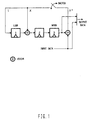
- FIG.2 is a block diagram showing a configuration of an arithmetic processing unit according to this embodiment.
- the arithmetic processing unit is mainly configured by operation data storage section 101 that stores operation data, input data storage section 102 that stores input data, generator polynomial storage section 103 that stores coefficients of a generator polynomial, operators 104 and 105 that carry out mod2 additions and selection section 106 that outputs either one of the two data items entered.
- operation data storage section 101 and generator polynomial storage section 103 are configured by at least N bits and operator 105 must have a capacity for performing at least N-bit mod2 additions.
- operation data storage section 101 and generator polynomial storage section 103 are configured by at least 3 bits and operator 105 carries out mod2 additions of at least 3 bits.
- operation data stored in operation data storage section 101 is assumed to be ⁇ a2, a1, a0 ⁇ with the MSB first, a2 corresponds to the boundary between the 3rd degree and 2nd degree, a1 corresponds to the boundary between the 2nd degree and 1st degree and a0 corresponds to the boundary between the 1st degree and 0th degree.
- input data which is a CRC target
- input data is output from the first 1 bit at a time every 1 machine cycle.
- first 1 bit at each point in time of input data stored in input data storage section 102 is ⁇ b ⁇ .
- coefficients of terms of the (highest degree - 1)th or lower degrees are stored in descending order with the highest degree being the MSB.
- Operator 104 carries out a mod2 addition between MSB ⁇ a2 ⁇ of operation data stored in operation data storage section 101 and input data ⁇ b ⁇ stored in input data storage section 102 and 1-bit operation result ⁇ a2 ⁇ b ⁇ is output to selection section 106.
- Operator 105 carries out a mod2 addition between data ⁇ a1, a0, 0 ⁇ obtained by shifting the operation data stored in operation data storage section 101 by 1 bit toward the MSB side (hereinafter referred to as "shift data") and coefficients ⁇ c2, c1, c0 ⁇ of the generator polynomial stored in generator polynomial storage section 103 and the operation result ⁇ a1 ⁇ c2, a0 ⁇ c1, 0 ⁇ c0 ⁇ is output to selection section 106.
- Selection section 106 selects either shift data ⁇ a1, a0, 0 ⁇ or operation result ⁇ a1 ⁇ c2, a0 ⁇ c1, 0 ⁇ c0 ⁇ of operator 105 based on operation result ⁇ a2 ⁇ b ⁇ of operator 104 and stores the selected one in operation data storage section 101 as new operation data ⁇ a2, a1, a0 ⁇ . For example, if the operation result of operator 104 is "0", selection section 106 stores the shift data in operation data storage section 101 and if the operation result of operator 104 is "1" selection section 106 stores the operation result of operator 105 in operation data storage section 101.
- FIG.3 shows a case with a 3-bit CRC and expresses operation data as A[2:0], the first 1 bit in each point in time of input data as B and the coefficients of the generator polynomial as C[2:0].
- operation data A[2:0] stored in storage section 101 is initialized to A(0,0,0), etc.
- input data which is a CRC target
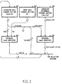
- FIG.4 is a block diagram showing a configuration of an arithmetic processing unit according to this embodiment.
- the components common to those in FIG.2 will be assigned the same reference numerals as those in FIG.2 and explanations thereof will be omitted.
- the arithmetic processing unit shown In FIG.4 adopts a configuration with selection sections 201 and 202, operator 203 and operation result storage section 204 added instead of operators 104 and 105.
- the arithmetic processing unit shown in FIG.4 assigns the processing by two operators 104 and 105 in the arithmetic processing unit shown in FIG.2 to operator 203 and executes a CRC operation in 2 machine cycles per 1 bit.
- Selection section 201 and selection section 202 switch data input to operator 203 in the 1st machine cycle and 2nd machine cycle.
- selection section 201 outputs the input data stored in input data storage section 102 to operator 203.
- Selection section 202 outputs the MSB of the operation data stored in operation data storage section 101 to operator 203.
- Operator 203 carries out a mod2 addition between the input data and the MSB of operation data and stores the operation result in operation result storage section 204.
- selection section 201 outputs the operation data stored in operation data storage section 101 to operator 203.
- Selection section 202 outputs coefficients of a generator polynomial stored in generator polynomial storage section 103 to operator 203.
- Operator 203 carries out a mod2 addition between the operation data and the coefficients of the generator polynomial and outputs the operation result to selection section 106.
- selection section 106 selects either the shift data or the operation result of operator 203 based on the operation result stored in operation result storage section 204 and stores the selected one in operation data storage section 101 as new operation data. For example, if the operation result stored in operation result storage section 204 is "0", selection section 106 stores the shift data in operation data storage section 101 and if the operation result is "1", selection section 106 stores the operation result of operator 105 in operation data storage section 101.
- this embodiment can perform CRC operations by the DSP more efficiently than conventional units and make it possible to implement the DSP on a single chip, reduce the size, weight and cost of the portable terminal and extend the life of the battery.
- the arithmetic processing unit can execute CRC operations in a time equivalent to 1 machine cycle per 1 bit of input data.
- FIG.5 is a block diagram showing a configuration of an arithmetic processing unit according to this embodiment.
- the components common to those in FIG.2 will be assigned the same reference numerals as those in FIG.2 and explanations thereof will be omitted.
- the arithmetic processing unit shown in FIG.5 adopts a configuration with operator 301 added instead of operators 104 and 105.
- the arithmetic processing unit shown in FIG.5 assigns the processing by two operators 104 and 105 in the arithmetic processing unit shown in FIG.2 to operator 301 and executes a CRC operation in 1 machine cycle per 1 bit by carrying out an operation after merging two kinds of data.
- operation data storage section 101 and generator polynomial storage section 103 are configured by at least 3 bits and operator 301 performs a mod2 addition of at least 4 bits.
- operation data stored in operation data storage section 101 is A[2:0]
- the first 1 bit at each point in time of Input data stored in input data storage section 102 is B
- coefficients of the generator polynomial stored in generator polynomial storage section 103 are C[2:0].
- One of the data entered in operator 301 is values ⁇ A[1], A[0], 0, B) resulting from a merge between data ⁇ A[1], A[0], 0 ⁇ obtained by logically shifting the operation data stored in operation data storage section 101 by 1 bit toward the MSB side and input data ⁇ B ⁇ of 1 bit stored in input data storage section 102.
- the other is values ⁇ C[2], C[1], C[0], A[2] ⁇ resulting from a merge between coefficients ⁇ C[2], C[1], C[0] ⁇ of the generator polynomial stored in generator polynomial storage section 103 and MSB ⁇ A[2] ⁇ of the operation data stored in operation data storage section 101.
- Operator 301 carries out a mod2 addition between ⁇ A[1], A[0], 0, B) and ⁇ C[2], C[1], C[0], A[2] ⁇ and outputs the addition result to selection section 106.
- Selection section 106 based on LSB ⁇ A[2] ⁇ B ⁇ of the operation result of operator 301, selects either shift data ⁇ A[1], A[0], 0 ⁇ or operation result ⁇ A[1] ⁇ C[2], A[0] ⁇ C[1], 0 ⁇ C[0] ⁇ other than the LSB of operator 301, and stores the selected one in operation data storage section 101 as new operation data ⁇ A[2:0] ⁇ .
- selection section 106 stores ⁇ A[1], A[0], 0 ⁇ in operation data storage section 101 and if ⁇ A[2] ⁇ B ⁇ is "1", selection section 106 stores ⁇ A[1] ⁇ C[2], A[0] ⁇ C[1], 0 ⁇ [0] ⁇ in operation data storage section 101.
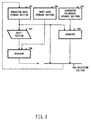
- FIG.6 is a block diagram showing a configuration of an arithmetic processing unit according to this embodiment.
- the components common to those in FIG.2 will be assigned the same reference numerals as those in FIG.2 and explanations thereof will be omitted.
- the arithmetic processing unit shown in FIG.6 adopts a configuration with shift section 401 added.
- Shift section 401 logically shifts operation data stored in operation data storage section 101 by a value (highest degree - 1) of the generator polynomial toward the LSB side and outputs the LSB value to operator 104.
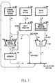
- FIG.7 is a block diagram showing a configuration of an arithmetic processing unit according to this embodiment.
- the components common to those in FIG.6 will be assigned the same reference numerals as those in FIG 6 and explanations thereof will be omitted.
- the arithmetic processing unit shown in FIG.7 configures operation data storage section 101 by general register 501, configures input data storage section 102 by RAM 502 and shift register 503, configures generator polynomial storage section 103 by ROM 504 and general register 505, configures shift section 401 by general shifter 506 and configures operator 105 by ALU (Arithmetic Logic Unit) 507.
- ALU Arimetic Logic Unit
- Input data is stored in RAM 502 in units of 16 bits, MSB-first for several words and 1-word input data B[15:0] is transferred to shift register 503 before a CRC operation is carried out.
- shift register 503 When a CRC operation is carried out, shift register 503 outputs the MSB value to operator 104 once every machine cycle and shifts up at the same time.
- At least one coefficient of a generator polynomial is stored in ROM 504 and the generator polynomial specified by the DSP beforehand is transferred to general register 505 before a CRC operation is carried out.
- ⁇ 0,1,1 ⁇ is stored in ROM 504.
- General shifter 506 logically shifts operation data A[15:0] stored in general register 501 by the value of (highest degree - 1) of the generator polynomial toward the LSB side and outputs the LSB value to operator 104. In this embodiment, general shifter 506 outputs A[2].
- Shift data ⁇ A[14:0],0 ⁇ which is a value obtained by logically shifting the operation data stored in general register 501 by 1 bit toward the MSB side, is always input to ALU 507 with fixed wiring. Moreover, coefficients C[15:0] of the generator polynomial stored in general register 505 are input to ALU 507. ALU 507 carries out a mod2 addition between ⁇ A[14:0],0 ⁇ and C[15:0] and outputs the operation result to selection section 106.
- selection section 106 selects either the operation result of ALU 507 or shift data and stores the selected one in general register 501 as new operation data. For example, if the operation result of operator 104 is "0" selection section 106 stores shift data in general register 501 and if the operation result of operator 104 is "1", selection section 106 stores the operation result of ALU 507 in general register 501.
- general registers 501 and 505 can store results of operations other than CRC operations in the process.
- Shift register 503 can also be used for DSP instructions other than CRC operations such as division instruction.
- general shifter 506 When executing shift operation instructions other than a CRC operation, general shifter 506 acquires data from a general register group or memory (RAM or ROM), etc., performs a shift operation and writes the operation results in a general register or memory, etc.
- a general register group or memory RAM or ROM
- ALU 507 When executing ALU operation instructions other than a CRC operation, ALU 507 acquires data from a general register group or memory (RAM or ROM), etc., performs ALU operation and writes the operation results in a general register or memory, etc.
- the higher-degree terms of the generator polynomial are stored on the MSB side, it is also possible to store those terms on the LSB side and add changes thereto accordingly.
- a channel decoding section of a radio communication base station apparatus or terminal apparatus can form a channel coding section, channel decoding section and timing control section, etc. on single-chip DSP software, making it possible to reduce the number of parts in the apparatus, reduce the size, weight or cost of the apparatus.
- the arithmetic processing unit of the present invention can repeatedly execute CRC operations in 1 or 2 machine cycles per 1 bit of input data, and therefore can perform CRC operations by the DSP efficiently, implement the DSP on a single-chip, reduce the size, weight and cost of the portable terminal and extend the life of the battery.
Landscapes
- Engineering & Computer Science (AREA)
- Physics & Mathematics (AREA)
- Theoretical Computer Science (AREA)
- General Physics & Mathematics (AREA)
- Computer Networks & Wireless Communication (AREA)
- Pure & Applied Mathematics (AREA)
- Mathematical Optimization (AREA)
- Mathematical Analysis (AREA)
- Probability & Statistics with Applications (AREA)
- Computational Mathematics (AREA)
- Signal Processing (AREA)
- Computing Systems (AREA)
- Mathematical Physics (AREA)
- General Engineering & Computer Science (AREA)
- Detection And Correction Of Errors (AREA)
- Error Detection And Correction (AREA)
- Complex Calculations (AREA)
Applications Claiming Priority (3)
| Application Number | Priority Date | Filing Date | Title |
|---|---|---|---|
| JP12267399A JP3607116B2 (ja) | 1999-04-28 | 1999-04-28 | 演算処理装置 |
| JP12267399 | 1999-04-28 | ||
| PCT/JP2000/002681 WO2000067125A1 (fr) | 1999-04-28 | 2000-04-25 | Processeur |
Publications (1)
| Publication Number | Publication Date |
|---|---|
| EP1096380A1 true EP1096380A1 (fr) | 2001-05-02 |
Family
ID=14841813
Family Applications (1)
| Application Number | Title | Priority Date | Filing Date |
|---|---|---|---|
| EP00919165A Withdrawn EP1096380A1 (fr) | 1999-04-28 | 2000-04-25 | Processeur |
Country Status (5)
| Country | Link |
|---|---|
| EP (1) | EP1096380A1 (fr) |
| JP (1) | JP3607116B2 (fr) |
| CN (1) | CN1300391A (fr) |
| AU (1) | AU3988100A (fr) |
| WO (1) | WO2000067125A1 (fr) |
Cited By (2)
| Publication number | Priority date | Publication date | Assignee | Title |
|---|---|---|---|---|
| EP1427109A2 (fr) * | 2002-12-04 | 2004-06-09 | STMicroelectronics Asia Pacific Pte Ltd | Appareil et méthode de calcul de la valeur de redondance cyclique pour un mot de données d'entrée à bits multiples |
| US6754870B2 (en) | 2000-04-14 | 2004-06-22 | Matsushita Electric Industrial Co., Ltd. | CRC operation unit and CRC operation method |
Families Citing this family (4)
| Publication number | Priority date | Publication date | Assignee | Title |
|---|---|---|---|---|
| EP1322846B1 (fr) | 2000-10-05 | 2006-07-12 | Nissan Motor Company, Limited | Regulation d'un compresseur de suralimentation |
| CN100517214C (zh) * | 2007-05-30 | 2009-07-22 | 北京天碁科技有限公司 | 一种实现二进制多项式运算的硬件配置方法及硬件系统 |
| CN102681818A (zh) * | 2011-03-09 | 2012-09-19 | 上海华虹集成电路有限责任公司 | 基于ucps加密算法的128比特模加电路及控制方法 |
| WO2019224955A1 (fr) * | 2018-05-23 | 2019-11-28 | 堺ディスプレイプロダクト株式会社 | Système de connexion |
Family Cites Families (2)
| Publication number | Priority date | Publication date | Assignee | Title |
|---|---|---|---|---|
| JPS51132048A (en) * | 1975-05-13 | 1976-11-16 | Mitsubishi Electric Corp | Computing circuit of cyclic code |
| JP3252029B2 (ja) * | 1993-08-04 | 2002-01-28 | 松下電器産業株式会社 | 符号化装置及び符号化方法 |
-
1999
- 1999-04-28 JP JP12267399A patent/JP3607116B2/ja not_active Expired - Fee Related
-
2000
- 2000-04-25 AU AU39881/00A patent/AU3988100A/en not_active Abandoned
- 2000-04-25 WO PCT/JP2000/002681 patent/WO2000067125A1/fr not_active Application Discontinuation
- 2000-04-25 CN CN 00800598 patent/CN1300391A/zh active Pending
- 2000-04-25 EP EP00919165A patent/EP1096380A1/fr not_active Withdrawn
Non-Patent Citations (1)
| Title |
|---|
| See references of WO0067125A1 * |
Cited By (2)
| Publication number | Priority date | Publication date | Assignee | Title |
|---|---|---|---|---|
| US6754870B2 (en) | 2000-04-14 | 2004-06-22 | Matsushita Electric Industrial Co., Ltd. | CRC operation unit and CRC operation method |
| EP1427109A2 (fr) * | 2002-12-04 | 2004-06-09 | STMicroelectronics Asia Pacific Pte Ltd | Appareil et méthode de calcul de la valeur de redondance cyclique pour un mot de données d'entrée à bits multiples |
Also Published As
| Publication number | Publication date |
|---|---|
| AU3988100A (en) | 2000-11-17 |
| JP2000311096A (ja) | 2000-11-07 |
| WO2000067125A1 (fr) | 2000-11-09 |
| JP3607116B2 (ja) | 2005-01-05 |
| CN1300391A (zh) | 2001-06-20 |
Similar Documents
| Publication | Publication Date | Title |
|---|---|---|
| US6754870B2 (en) | CRC operation unit and CRC operation method | |
| US4937828A (en) | High speed parallel CRC device for concatenated data frames | |
| US6697994B2 (en) | Operation processing apparatus and operation processing method | |
| US5970097A (en) | Arithmetic apparatus for use in Viterbi decoding | |
| JP4071879B2 (ja) | 誤り検出器、この誤り検出器を備えた通信システム、および誤り検出方法 | |
| US7216285B2 (en) | System and method for generating cyclic redundancy check | |
| EP1096380A1 (fr) | Processeur | |
| EP1146652B1 (fr) | Codeur à haute vitesse pour codes convolutifs | |
| KR100864363B1 (ko) | 부호화 회로 및 디지털 신호 처리 회로 | |
| US6725415B2 (en) | Arithmetic unit performing cyclic redundancy check at high speed | |
| JP2000004169A (ja) | Crc演算方法及びcrc演算回路 | |
| AU758068B2 (en) | Fast metric calculation for viterbi decoder implementation | |
| EP1322041A1 (fr) | Décodeur Viterbi utilisant un treillis restructuré | |
| JPH06121172A (ja) | 画像符号化装置 | |
| US6718514B2 (en) | Parity checking device and method in data communication system | |
| JP3452345B2 (ja) | 演算処理装置とその利用装置 | |
| JP3521558B2 (ja) | 伝送装置 | |
| US6470369B1 (en) | Euclid mutual division arithmetic circuit and processing circuit | |
| JP2001186021A (ja) | 誤り検出装置及びそれを内蔵した演算処理装置 | |
| JPH06112848A (ja) | ビタビ復号用演算装置 | |
| KR20010019289A (ko) | 전송에러 검출기의 부분적 가산기 | |
| JPH10178356A (ja) | 演算処理装置及びそれを用いた無線局装置 | |
| JP2003234656A (ja) | 演算処理装置 | |
| JPH01206731A (ja) | シーケンシャル復号器 | |
| JP2003204271A (ja) | ディジタル信号処理プロセッサ |
Legal Events
| Date | Code | Title | Description |
|---|---|---|---|
| PUAI | Public reference made under article 153(3) epc to a published international application that has entered the european phase |
Free format text: ORIGINAL CODE: 0009012 |
|
| 17P | Request for examination filed |
Effective date: 20010118 |
|
| AK | Designated contracting states |
Kind code of ref document: A1 Designated state(s): AT BE CH CY DE DK ES FI FR GB GR IE IT LI LU MC NL PT SE |
|
| STAA | Information on the status of an ep patent application or granted ep patent |
Free format text: STATUS: THE APPLICATION HAS BEEN WITHDRAWN |
|
| 18W | Application withdrawn |
Effective date: 20030128 |