EP1096262A2 - Current detector - Google Patents
Current detector Download PDFInfo
- Publication number
- EP1096262A2 EP1096262A2 EP00123137A EP00123137A EP1096262A2 EP 1096262 A2 EP1096262 A2 EP 1096262A2 EP 00123137 A EP00123137 A EP 00123137A EP 00123137 A EP00123137 A EP 00123137A EP 1096262 A2 EP1096262 A2 EP 1096262A2
- Authority
- EP
- European Patent Office
- Prior art keywords
- current
- transistor
- circuit
- transistors
- voltage
- Prior art date
- Legal status (The legal status is an assumption and is not a legal conclusion. Google has not performed a legal analysis and makes no representation as to the accuracy of the status listed.)
- Granted
Links
- 238000001514 detection method Methods 0.000 claims description 72
- 230000003213 activating effect Effects 0.000 claims description 3
- 230000004913 activation Effects 0.000 abstract description 7
- 230000008859 change Effects 0.000 description 18
- 230000004048 modification Effects 0.000 description 17
- 238000012986 modification Methods 0.000 description 17
- 238000010586 diagram Methods 0.000 description 14
- 230000014509 gene expression Effects 0.000 description 12
- 238000000034 method Methods 0.000 description 11
- 235000012431 wafers Nutrition 0.000 description 11
- 230000008569 process Effects 0.000 description 8
- 230000007257 malfunction Effects 0.000 description 5
- 230000003071 parasitic effect Effects 0.000 description 5
- 238000006243 chemical reaction Methods 0.000 description 4
- 239000004065 semiconductor Substances 0.000 description 4
- 238000009792 diffusion process Methods 0.000 description 3
- 238000004519 manufacturing process Methods 0.000 description 3
- 230000015572 biosynthetic process Effects 0.000 description 2
- 238000005530 etching Methods 0.000 description 2
- 239000012535 impurity Substances 0.000 description 2
- 230000004044 response Effects 0.000 description 2
- 230000003321 amplification Effects 0.000 description 1
- 230000008901 benefit Effects 0.000 description 1
- 230000000694 effects Effects 0.000 description 1
- 230000005669 field effect Effects 0.000 description 1
- 238000012544 monitoring process Methods 0.000 description 1
- 238000003199 nucleic acid amplification method Methods 0.000 description 1
- 102220015875 rs6734111 Human genes 0.000 description 1
- 229910052710 silicon Inorganic materials 0.000 description 1
- 239000010703 silicon Substances 0.000 description 1
Images



Classifications
-
- G—PHYSICS
- G01—MEASURING; TESTING
- G01R—MEASURING ELECTRIC VARIABLES; MEASURING MAGNETIC VARIABLES
- G01R19/00—Arrangements for measuring currents or voltages or for indicating presence or sign thereof
- G01R19/165—Indicating that current or voltage is either above or below a predetermined value or within or outside a predetermined range of values
Definitions
- This invention relates to a current detector for detecting a supply current supplied to a load with good accuracy.
- a high-accuracy current detector has been demanded for the purposes of finding the charge amount of a secondary battery used with a personal computer, etc., with good accuracy, monitoring a current distribution circuit in an automobile, etc.
- a method of placing a shunt resistor of a high-accuracy low resistance element in series with wiring through which the current to be detected flows and detecting a voltage drop occurring in the shunt resistor, thereby detecting a current value is known.
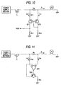
- a current I12 proportional to a load current IL flowing into a shunt resistor Rs is formed using pnp transistors Q11 and Q12 and a resistor R11 and is converted into an output current VOUT using a resistor R12, thereby detecting the load current IL.
- I14 ⁇ R14 (I13+IL) ⁇ RS ⁇ IL ⁇ RS
- R14 is the resistance value of a resistor R14
- RS is the resistance value of a shunt resistor Rs
- I13 is a current flowing into the inversion input terminal of the operational amplifier OP1
- I14 is a current flowing into the noninversion input terminal of the operational amplifier OP1.
- the collector current I14 of a pnp transistor Q13 becomes I14 ⁇ Il ⁇ RS/R14 and a current proportional to load current IL can be output.
- a current detector using a current detection resistor placed between a power supply section and a load to detect a supply current value supplied from the power supply section to the load comprising a first resistance element having a first resistance value of a predetermined magnification of a resistance value of the current detection resistor, a first current mirror circuit made up of a plurality of negative-polarity-type transistors and having one end connected to an end part of the current detection resistor on the power supply section side thereof via the first resistance element and an opposite end connected to an end part of the current detection resistor on the load side thereof, a second current mirror circuit made up of a plurality of positive-polarity-type transistors and having both input ends connected to both output ends of the first current mirror circuit, a second resistance element placed between at least either of both output ends of the second current mirror circuit and ground and having a second resistance value, and current detection means for detecting a voltage of the second resistance element on the second current mirror circuit 8 side thereof, characterized by switch means being
- the current detector of the invention further includes current value detection means using the detected voltage to find the supply current value.
- the negative-polarity-type transistors are transistors (current control elements) such as pnp transistors and p-channel FETs (field-effect transistors) of the type wherein when a current is drawn out from a control terminal, current terminals are brought into conduction
- the positive-polarity-type transistors are transistors (current control elements) such as npn transistors and n-channel FETs of the type wherein when a current is input to a control terminal, current terminals are brought into conduction.
- the control terminals of the transistors making up the second current mirror circuit are connected to one input end of the second current mirror circuit and the control terminals of the transistors making up the first current mirror circuit are connected to an opposite input end of the second current mirror circuit.
- the control terminals of the transistors making up the first current mirror circuit are grounded through the switch means, whereby a current is forcibly made to flow into the control terminals, so that it is made possible to make the circuit operation at the activation time reliable.
- a part of load current is shunted with good accuracy via the first resistance element having the first resistance value of the predetermined magnification of the resistance value of the current detection resistor, the first current mirror circuit, and the second current mirror circuit, and the output end of the shunted current is grounded via the second resistance element having the second resistance value, so that an output voltage proportional to the load current can be obtained with good accuracy from the second resistance element in a simple configuration and the load current can be found with good accuracy from the output voltage.
- the switch means comprises a transistor circuit capable of grounding the control terminal of the transistor.
- the switch means can be easily implemented as transistor circuit.
- the switch means comprises a one-shot pulse generation circuit for activating the transistor circuit.
- a one-shot pulse from the one-shot pulse generation circuit can be used easily to turn off the transistor circuit after turning on the transistor circuit only for a predetermined time.
- the current detector of the invention further includes control means for controlling so that the voltage detection means detects the voltage after on/off control of the switch means is performed (in the embodiment, control means 11 or microcomputer 11a).
- control means controls so as to detect the voltage every constant period and performs on/off control of the switch means every constant period while the voltage is not detected.
- on/off control of the switch means is performed every constant period.
- the current voltage conversion circuit made up of the first and second current mirror circuits malfunctions and stops due to noise, etc., for example, it is again activated in the next period and the detected voltage can always be monitored. Therefore, noise resistance of the first and second current mirror circuits is enhanced.
- the first current mirror circuit comprises a first transistor having an emitter connected to the power supply section side of the current detection resistor via the first resistance element and a second transistor having an emitter connected to the load side of the current detection resistor and a base and a collector connected to a base of the first transistor, the first and second transistors being implemented as pnp transistors
- the second current mirror circuit comprises a third transistor having a collector connected to a collector of the first transistor and a fourth transistor having a collector connected to the collector of the second transistor and a base connected to a base and the collector of the third transistor, the third and fourth transistors being implemented as npn transistors, and an emitter of at least either of the third and fourth transistors is grounded via the second resistance element.
- the first and second current mirror circuits can be configured more easily.
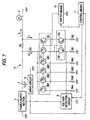
- the current detector of the invention further includes a third resistance element having the second resistance value, a fourth resistance element having the same resistance value as the first resistance element, and a fifth resistance element having a resistance value different from the second resistance value
- the first current mirror circuit further includes a fifth transistor of a pnp transistor having an emitter connected to the power supply section side of the current detection resistor via the fourth resistance element and a base connected to the base of the first transistor, wherein the third transistor has the emitter grounded via the second resistance element, the fourth transistor has the emitter grounded via the third resistance element, and the fifth transistor has a collector grounded via the fifth resistance element, and wherein the voltage detection means further detects a voltage value of the collector of the fifth transistor.
- the load current can be found suitable with good accuracy if the voltage range that can be detected by the voltage detection means is narrow as compared with the change range of the detected voltage caused by change in the load current. Also in this case, it is made possible to make the circuit operation at the activation time reliable by the switch means.
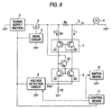
- the current detector of the invention further includes a predetermined number of sixth resistance elements each having the second resistance value, wherein the first current mirror circuit has the predetermined number of sixth transistors of pnp transistors having emitters connected to the emitter of the first transistor and bases connected to the base of the first transistor, and wherein collectors of the sixth transistors are grounded via the sixth resistance elements.
- the currents flowing into the second resistance element and the sixth resistance elements become equal levels to each other, thus the detected voltage becomes low and the voltage detection means can be made up of circuit parts consuming low power and the circuit can be miniaturized and the costs can be reduced. Also in this case, it is made possible to make the circuit operation at the activation time reliable by the switch means.
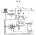
- FIG. 1 is a diagram to show the configuration of a current supply unit containing a current detector of one embodiment of the invention.
- a current supply unit 1 comprises an FET 3 for current supply and a load 4 connected in series between a power supply section 2 and ground, wherein the FET 3 is controlled based on a drive current from a drive circuit 5 for supplying a load current IL from the power supply section 2 to the load 4.
- a current detector 6 is placed between the FET 3 and the load 4 for detecting the load current IL supplied from the power supply section 2 to the load 4.
- the current detector 6 comprises a shunt resistor Rs (current detection resistor) placed between the FET 3 and the load 4, a resistor R1 (first resistance element) connected to the FET 3 side of the shunt resistor Rs, a first current mirror circuit 7, a second current mirror circuit 8, a resistor R2 (second resistance element) placed between both output ends of the second current mirror circuit 8 and ground, and a voltage detection circuit 9 for detecting an output voltage VOUT of the resistor R2 on the second current mirror circuit 8 side thereof and using the output voltage VOUT to determine whether or not the load current is within the normal range, and converts a current proportional to the load current IL into a voltage with the resistor R2 from the shunt resistor Rs through the first current mirror circuit 7 and the second current mirror circuit 8, and the voltage detection circuit 9 detects the voltage.
- Rs current detection resistor
- the current detector 6 further comprises switch means 10 placed between control terminals (bases) of transistors making up the first current mirror circuit 7 and ground and control means 11 for controlling so as to cause the voltage detection circuit 9 to output a voltage detection start signal after the switch means 10 is turned on/off.
- the shunt resistor R2 is a high-accuracy low resistance element having a known resistance value RS and provides a current detection resistor.
- the resistor R1 has a first resistance value of a predetermined magnification of the resistance value of the shunt resistor Rs.
- the first current mirror circuit 7 has one input end connected to one end of the shunt resistor Rs on the power supply section 2 side thereof via the first resistance element and an opposite input end connected to one end of the shunt resistor Rs on the load 4 side thereof.
- the first current mirror circuit 7 is made up of a transistor Q1 (first transistor) and a transistor Q2 (second transistor) which are pnp transistors having the same transistor characteristic.
- the transistor Q1 has an emitter connected to the power supply section 2 side of the shunt resistor Rs via the resistor R1 and a base connected to a base and a collector of the transistor Q2 and the transistor Q2 has an emitter connected to the load 4 side of the shunt resistor Rs.
- the emitter sides of the transistors Q1 and Q2 form both input ends of the first current mirror circuit 7 and the collector sides of the transistors Q1 and Q2 form both output ends of the first current mirror circuit 7.
- the second current mirror circuit 8 is made up of a transistor Q3 (third transistor) and a transistor Q4 (fourth transistor) which are npn transistors having the same transistor characteristic.
- the transistor Q3 has a collector connected to the collector of the first transistor Q1 and a base connected to the collector of the transistor Q3 and a base of the transistor Q4 and the transistor Q4 has a collector connected to the collector of the transistor Q2.
- the collector sides of the transistors Q3 and Q4 form both input ends of the second current mirror circuit 8 and the emitter sides of the transistors Q3 and Q4 form both output ends of the second current mirror circuit 8.
- the transistor group T1 consisting of the pnp transistors Q1 and Q2 and the transistor group T2 consisting of the npn transistors Q3 and Q4 have the same transistor characteristics such that the base-emitter voltage Vbe difference can be almost ignored by using adjacent transistors on the same semiconductor wafer, etc.
- one package housing two adjacent transistors is commercially available and thus may be used.
- transistors Q1 and Q2 are placed adjacent to each other and transistors Q3 and Q4 are placed adjacent to each other on semiconductor wafer, whereby the base-emitter voltage Vbe difference can be placed at a level to such an extent that it can be almost ignored.
- the resistor R2 has a second resistance value and is placed between the emitters of the transistors Q3 and Q4 and ground.
- the voltage detection circuit 9 forms voltage detection means for detecting the output voltage VOUT of the emitters of the transistors Q3 and Q4. It also forms load current determination means (current value detection means) for using the detected voltage value to determine whether or not the load current IL is within the normal range. Specifically, for example, if the voltage detection circuit 9 is implemented as one comparator, the comparator can compare the output voltage VOUT with the reference voltage (lower or upper limit reference voltage) and whether or not the load current IL is within the normal range can be determined by output of the comparator. If the voltage detection circuit 9 is made up of two comparators, the first comparator can compare the output voltage VOUT with the lower limit reference voltage and whether or not the load current IL is within the lower limit range can be determined by output of the first comparator.
- the second comparator can compare the output voltage VOUT with the upper limit reference voltage and whether or not the load current IL is within the upper limit range can be determined by output of the second comparator.
- Outputs of the first and second comparators can be input to an AND gate and whether or not the load current IL is within the normal range can be determined by output of the AND gate.
- the switch means 10 has a transistor circuit 101 and a one-shot pulse generation circuit 102 for activating the transistor circuit 101, as shown in FIG. 2.
- the transistor circuit 101 comprises a transistor Q8, which has a collector connected via a resistor R6 to the bases of the transistors Q1 and Q2 and an emitter grounded.
- the one-shot pulse generation circuit 102 has an output end connected to a base of the transistor Q8 and outputs a one-shot pulse of a predetermined duration to the base of the transistor Q8 as a trigger signal is input to an input end of the one-shot pulse generation circuit 102.
- Power supply Vcc is supplied to the one-shot pulse generation circuit 102 from the power supply section 2.
- the control means 11 controls so as to output a trigger signal as a circuit drive signal to the one-shot pulse generation circuit 102 only once when the power is turned on and after the expiration of a predetermined time, the control means 11 controls so as to output a drive start signal of the voltage detection circuit 9.
- the reason why the switch means 10 is provided is as follows: If a route where a base current flows into the base of the transistor Q1 or Q2 does not exist, the circuit does not operate. If the switch means 10 is not provided, the first current mirror circuit 7 and the second current mirror circuit 8 can operate, but the stability of the operation is not sufficient. That is, in the actual circuit operation, current IL0 shown in FIG. 1 flowing because of a voltage drop occurring in the shunt resistor Rs causes the transistor Q1 to allow a collector current to flow, which then becomes a base current of the transistors Q3 and Q4 at the following stage, and currents I1 and I2 flow into the first current mirror circuit 7 and the second current mirror circuit 8.
- the first current mirror circuit 7 and the second current mirror circuit 8 operate.
- the circuit may operate due to the collector leakage current of each transistor.
- the above-described circuit operation is realized based on the internal structure (parasitic capacitance) of each of the actual transistors and the stable operation is not reliably performed depending on the combination of the transistors and the circuit constants. A malfunction caused by noise or temperature change (circuit stop caused by parasitic capacitance change, etc.,) can also occur. Therefore, to perform the stable circuit operation reliably, the circuit is grounded via the switch means 10 when the circuit is started, whereby the route where the base current flows into the bases of the transistors Q1 and Q2 is forcibly provided.
- the transistor Q8 As the transistor Q8 is turned on, the base current is made to flow into the bases of the transistors Q1 and Q2 and the first current mirror circuit 7 and the second current mirror circuit 8 are forcibly operated.
- the transistor Q8 When the transistor Q8 is on, the bases of the transistors Q1 and Q2 are grounded, thus voltage not related to the load current IL (voltage not proportional to the load current IL) is output as the output voltage VOUT.
- the output voltage VOUT is not monitored by the voltage detection circuit 9.
- I2 ⁇ R1 + Vbe(Q1) (I1 + IL) ⁇ RS + Vbe(Q2)
- I1 is the collector current flowing into the transistor Q2
- I2 is the collector current flowing into the transistor Q1
- Vbe(Q1) is the base-emitter voltage of the transistor Q1
- Vbe(Q2) is the base-emitter voltage of the transistor Q2, as shown in FIG. 1.
- the transistors Q3 and Q4 make up so-called current mirror circuit.
- hFE (collector current)/(base current) of transistor is sufficiently large, thus the emitter current and the collector current of each transistor can be assumed to be equal, and the following expressions 6, 7, and 8 are obtained:
- IC(Q3) I2
- IC(Q4) I1
- IC(Q3) IE(Q3)
- IC(Q4) IE(Q4)
- the operation of the circuitry having the configuration described above is as follows: First, when the power is turned on, the power supply section 2 is driven, driving the drive circuit 5 is also started, and driving the control means 11 is also started. When the drive circuit 5 is driven, the FET 3 is turned on and the load current IL is supplied to the load 4 via the shunt resistor Rs.
- the control means 11 When the control means 11 is driven, it outputs a trigger signal to the one-shot pulse generation circuit 102 and upon reception of the trigger signal, the one-shot pulse generation circuit 102 outputs a one-shot pulse to the base of the transistor Q8, whereby the transistor Q8 is turned on only for a predetermined time, the bases of the transistors Q1 and Q2 are grounded, a base current flows into the bases of the transistors Q1 and Q2, and the first current mirror circuit 7 and the second current mirror circuit 8 are forcibly operated.
- control means 11 controls so as to output a drive start signal of the voltage detection circuit 9, and the voltage detection circuit 9 monitors and detects the output voltage VOUT.
- the voltage detection circuit 9 finds the load current IL from the detected output voltage VOUT by the load current determination means and determines whether or not the load current IL is within the normal range. Determination display can be produced and the value of the load current IL can be displayed in response to the determination result.
- FIG. 3A is a drawing to show change in the load current IL from 5 (A) to 50 (A) and there are no units on the horizontal axis.
- FIG. 3B is a comparison drawing of change in (load current IL)/(output voltage VOUT) between the circuits in FIGS. 1 and 10 when the load current IL changes as in FIG. 3A.
- the minimum value and the maximum value of (IL)/(VOUT) in the circuit in FIG. 1 are 23.4 an 24.8 respectively, and the minimum value and the maximum value of (IL)/(VOUT) in the circuit in FIG. 10 are 19.8 an 23.75 respectively.
- the circuit operation at the starting time can be made reliable. That is, according to the embodiment, in the structure wherein the first current mirror circuit 7 and the second current mirror circuit 8 are simply connected, the circuit operation is realized based on the internal structure (parasitic capacitance) of each of the actual transistors and the stable operation is not reliably performed depending on the combination of the transistors and the circuit constants and a malfunction caused by noise, temperature change, etc., (circuit stop caused by parasitic capacitance change, etc.,) also occurs; however, according to the embodiment, the problems can be resolved.
- the transistor Q1 is connected to the power supply section 1 side of the shunt resistor Rs via the resistor R1
- the transistor Q2 is connected to the load 4 side of the shunt resistor Rs
- the transistors Q3 and Q4 making up the second current mirror circuit 8 are connected to the transistors Q1 and Q2, whereby a part of the load current IL is shunted with good accuracy and the output end of the shunted current is grounded via the resistor R2, so that the voltage proportional to the load current IL can be provided with good accuracy and the load current IL can be found with good accuracy accordingly.
- the control terminals of the transistors making up the first current mirror circuit are grounded through the switch means, whereby a current is forcibly made to flow into the control terminals, so that the circuit operation can be made reliable at the activation time.
- a part of load current is shunted with good accuracy via the first resistance element having the first resistance value of the predetermined magnification of the resistance value of the current detection resistor, the first current mirror circuit, and the second current mirror circuit, and the output end of the shunted current is grounded via the second resistance element having the second resistance value, so that an output voltage proportional to the load current can be obtained with good accuracy from the second resistance element and the load current can be found with good accuracy from the output voltage.
- the switch means for grounding the control terminals of the transistors of the first current mirror circuit can be easily implemented as transistor circuit.
- a one-shot pulse from the one-shot pulse generation circuit can be used easily to turn off the transistor circuit after turning on the transistor circuit only for a predetermined time.
- control means controls so as to output a current detection start signal to the voltage detection means after on/off control of the switch means is performed, so that the voltage detection timing can be taken reliably and well.
- on/off control of the switch means is performed every constant period.
- the current voltage conversion circuit made up of the first and second current mirror circuits malfunctions and stops due to noise, etc., for example, it is again activated in the next period and the detected voltage can always be monitored. Therefore, noise resistance of the first and second current mirror circuits can be enhanced.
- the first and second current mirror circuits can be configured easily.
- the load current can be found suitable with good accuracy. Also in this case, the circuit operation can be made reliable at the activation time by the switch means.
- the currents flowing into the second resistance element and the sixth resistance elements become equal levels to each other, so that the voltage detection means can be made up of circuit parts consuming low power and the circuit can be miniaturized and the costs can be reduced. Also in this case, the circuit operation can be made reliable at the activation time by the switch means.
Landscapes
- Physics & Mathematics (AREA)
- General Physics & Mathematics (AREA)
- Measurement Of Current Or Voltage (AREA)
- Control Of Electrical Variables (AREA)
- Control Of Voltage And Current In General (AREA)
Abstract
Description
Claims (9)
- A current detector using a current detection resistor placed between a power supply section and a load to detect a supply current value supplied from said power supply section to said load,said current detector comprising:a first resistance element having a first resistance value of a predetermined magnification of a resistance value of said current detection resistor,a first current mirror circuit made up of a plurality of negative-polarity-type transistors, and having one end connected to an end part of said current detection resistor on said power supply section side thereof via said first resistance element and an opposite end connected to an end part of said current detection resistor on said load side thereof,a second current mirror circuit made up of a plurality of positive-polarity-type transistors and having both input ends connected to both output ends of said first current mirror circuit,a second resistance element placed between at least either of both output ends of said second current mirror circuit and ground, and having a second resistance value,current detection means for detecting a voltage of said second resistance element on said second current mirror circuit side thereof, andswitch means placed between control terminals of said transistors making up said first current mirror circuit and ground.
- The current detector as claimed in claim 1, further comprising:current value detection means using the detected voltage to find the supply current value.
- The current detector as claimed in claim 1 or 2, whereinsaid switch means comprises: a transistor circuit capable of grounding the control terminal of said transistor.
- The current detector as claimed in claim 3, whereinsaid switch means comprises: a one-shot pulse generation circuit for activating said transistor circuit.
- The current detector as claimed in any of claims 1 to 4, further comprising:control means for controlling so that said voltage detection means detects the voltage after on/off control of said switch means is performed.
- The current detector as claimed in claim 5, whereinsaid control means controls so as to detect the voltage every constant period, and performs on/off control of said switch means every constant period while the voltage is not detected.
- The current detector as claimed in any of claims 1 to 6, whereinsaid first current mirror circuit comprises:a first transistor having an emitter connected to said power supply section side of said current detection resistor via said first resistance element, anda second transistor having an emitter connected to said load side of said current detection resistor and a base and a collector connected to a base of said first transistor, said first and second transistors being implemented as pnp transistors, whereinsaid second current mirror circuit comprises:a third transistor having a collector connected to a collector of said first transistor, anda fourth transistor having a collector connected to the collector of said second transistor and a base connected to a base and the collector of said third transistor, said third and fourth transistors being implemented as npn transistors, and whereinan emitter of at least either of said third and fourth transistors is grounded via said second resistance element.
- The current detector as claimed in claim 7, further comprising:a third resistance element having the second resistance value,a fourth resistance element having the same resistance value as said first resistance element, anda fifth resistance element having a resistance value different from the second resistance value, whereinsaid first current mirror circuit further includes:a fifth transistor of a pnp transistor having an emitter connected to said power supply section side of said current detection resistor via said fourth resistance element and a base connected to the base of said first transistor, and whereinsaid third transistor has the emitter grounded via said second resistance element,said fourth transistor has the emitter grounded via said third resistance element, andsaid fifth transistor has a collector grounded via said fifth resistance element, and whereinsaid voltage detection means further detects a voltage value of the collector of said fifth transistor.
- The current detector as claimed in claim 7, further comprising:a predetermined number of sixth resistance elements each having the second resistance value, whereinsaid first current mirror circuit has the predetermined number of sixth transistors of pnp transistors having emitters connected to the emitter of said first transistor and bases connected to the base of said first transistor, and whereincollectors of the sixth transistors are grounded via said sixth resistance elements.
Applications Claiming Priority (2)
| Application Number | Priority Date | Filing Date | Title |
|---|---|---|---|
| JP30540699A JP3417891B2 (en) | 1999-10-27 | 1999-10-27 | Current detector |
| JP30540699 | 1999-10-27 |
Publications (3)
| Publication Number | Publication Date |
|---|---|
| EP1096262A2 true EP1096262A2 (en) | 2001-05-02 |
| EP1096262A3 EP1096262A3 (en) | 2004-01-02 |
| EP1096262B1 EP1096262B1 (en) | 2008-06-18 |
Family
ID=17944754
Family Applications (1)
| Application Number | Title | Priority Date | Filing Date |
|---|---|---|---|
| EP00123137A Expired - Lifetime EP1096262B1 (en) | 1999-10-27 | 2000-10-25 | Current detector |
Country Status (4)
| Country | Link |
|---|---|
| US (1) | US6316967B1 (en) |
| EP (1) | EP1096262B1 (en) |
| JP (1) | JP3417891B2 (en) |
| DE (1) | DE60039217D1 (en) |
Cited By (6)
| Publication number | Priority date | Publication date | Assignee | Title |
|---|---|---|---|---|
| WO2002041491A1 (en) * | 2000-11-16 | 2002-05-23 | Robert Bosch Gmbh | A current-sensing switching circuit |
| EP1816483A1 (en) * | 2006-02-03 | 2007-08-08 | Siemens Aktiengesellschaft | Short-circuit and overcurrent detection circuit |
| EP2239591A1 (en) * | 2009-04-08 | 2010-10-13 | Alcatel Lucent | Current monitor for sensing the current in a current path and corresponding control device |
| WO2011064589A1 (en) * | 2009-11-27 | 2011-06-03 | Trw Limited | Motor control circuitry |
| DE112011100594B4 (en) * | 2010-02-18 | 2015-09-03 | Tridonic Ag | LED voltage measurement |
| EP2991088A1 (en) * | 2014-08-29 | 2016-03-02 | Marquardt Mechatronik GmbH | Electric switch |
Families Citing this family (17)
| Publication number | Priority date | Publication date | Assignee | Title |
|---|---|---|---|---|
| DE10038321A1 (en) * | 2000-08-05 | 2002-02-14 | Philips Corp Intellectual Pty | Adaptation circuit for audio and video signals |
| DE10258766B4 (en) * | 2002-12-16 | 2005-08-25 | Infineon Technologies Ag | Circuit arrangement for controlling and detecting the load current through a load |
| DE10301823A1 (en) * | 2003-01-20 | 2004-07-29 | Robert Bosch Gmbh | Battery available charge determination method, in which the charge remaining up to a defined limit is determined using a mathematical model of the battery, the inputs to which are determined from battery operating values |
| JP4581986B2 (en) * | 2005-12-15 | 2010-11-17 | パナソニック電工株式会社 | Detector and discharge lamp lighting device |
| JP4941718B2 (en) * | 2006-11-24 | 2012-05-30 | 横河電機株式会社 | Voltage shift circuit |
| DE502007002863D1 (en) * | 2007-04-16 | 2010-04-01 | Siemens Ag | Circuit for load current measurement, limiting and switching |
| JP5448813B2 (en) * | 2007-05-22 | 2014-03-19 | パナソニック株式会社 | Switching power supply |
| US8624610B2 (en) * | 2011-02-23 | 2014-01-07 | Texas Instruments Incorporated | Synthesized current sense resistor for wide current sense range |
| CN102426285B (en) * | 2011-09-14 | 2013-07-17 | 深圳航天科技创新研究院 | Current sensor used for bidirectional current sampling |
| US20130271102A1 (en) * | 2012-04-12 | 2013-10-17 | Roger Lin | Power supply control structure |
| JP5612024B2 (en) * | 2012-06-04 | 2014-10-22 | 大光電気株式会社 | High side current detection circuit |
| US10365329B2 (en) | 2016-05-26 | 2019-07-30 | Infineon Technologies Ag | Measurements in switch devices |
| KR101847839B1 (en) * | 2016-09-21 | 2018-04-11 | 현대자동차주식회사 | Apparatus for controlling electric current for vehicle and vehicle having the same |
| KR102463174B1 (en) | 2017-07-31 | 2022-11-04 | 삼성전자주식회사 | Reconfigurable amplifier and amplifying method thereof |
| CN112630498B (en) * | 2020-12-08 | 2024-06-11 | 中国空间技术研究院 | High-side sampling circuit |
| CZ309064B6 (en) * | 2021-03-24 | 2022-01-05 | České vysoké učení technické v Praze | Connection with current mirrors, method of impedance measurement and method of current to voltage conversion in this connection |
| CN116660614B (en) * | 2023-08-01 | 2023-09-22 | 苏州贝克微电子股份有限公司 | Voltage detection circuit for improving switching speed |
Family Cites Families (13)
| Publication number | Priority date | Publication date | Assignee | Title |
|---|---|---|---|---|
| JPH01212364A (en) * | 1988-02-19 | 1989-08-25 | Matsushita Electric Ind Co Ltd | Load current detection circuit |
| JPH0574982A (en) | 1991-09-17 | 1993-03-26 | Seiko Epson Corp | Semiconductor package |
| JPH05208645A (en) | 1991-11-26 | 1993-08-20 | Tokai Rika Co Ltd | Auxiliary power supply unit for vehicle |
| JPH07248342A (en) * | 1994-03-11 | 1995-09-26 | Nippon Motorola Ltd | Overcurrent detection circuit |
| US5955874A (en) * | 1994-06-23 | 1999-09-21 | Advanced Micro Devices, Inc. | Supply voltage-independent reference voltage circuit |
| US5498984A (en) * | 1994-09-30 | 1996-03-12 | Maxim Integrated Products | High side, current sense amplifier using a symmetric amplifier |
| US5627490A (en) * | 1995-02-23 | 1997-05-06 | Matsushita Electric Industrial Co., Ltd. | Amplifier circuit |
| JPH08272468A (en) * | 1995-03-29 | 1996-10-18 | Mitsubishi Electric Corp | Reference voltage generation circuit |
| JP3314591B2 (en) | 1995-08-31 | 2002-08-12 | 株式会社豊田自動織機 | Automotive power supply |
| JP3039454B2 (en) * | 1997-06-23 | 2000-05-08 | 日本電気株式会社 | Reference voltage generation circuit |
| JPH11160368A (en) * | 1997-12-02 | 1999-06-18 | Tdk Corp | Current detection circuit |
| JP3676595B2 (en) | 1998-11-13 | 2005-07-27 | 株式会社オートネットワーク技術研究所 | Current detection circuit |
| JP2000261260A (en) * | 1999-03-10 | 2000-09-22 | Mitsumi Electric Co Ltd | Voltage / current conversion circuit |
-
1999
- 1999-10-27 JP JP30540699A patent/JP3417891B2/en not_active Expired - Fee Related
-
2000
- 2000-10-20 US US09/692,144 patent/US6316967B1/en not_active Expired - Lifetime
- 2000-10-25 EP EP00123137A patent/EP1096262B1/en not_active Expired - Lifetime
- 2000-10-25 DE DE60039217T patent/DE60039217D1/en not_active Expired - Lifetime
Cited By (12)
| Publication number | Priority date | Publication date | Assignee | Title |
|---|---|---|---|---|
| WO2002041491A1 (en) * | 2000-11-16 | 2002-05-23 | Robert Bosch Gmbh | A current-sensing switching circuit |
| US7362010B2 (en) | 2000-11-16 | 2008-04-22 | Robert Bosch Gmbh | Currents-sensing switching circuit |
| EP1816483A1 (en) * | 2006-02-03 | 2007-08-08 | Siemens Aktiengesellschaft | Short-circuit and overcurrent detection circuit |
| CN101013810B (en) * | 2006-02-03 | 2011-04-06 | 西门子公司 | Short-circuit and overcurrent detection circuit |
| EP2239591A1 (en) * | 2009-04-08 | 2010-10-13 | Alcatel Lucent | Current monitor for sensing the current in a current path and corresponding control device |
| WO2010115681A1 (en) * | 2009-04-08 | 2010-10-14 | Alcatel Lucent | Current monitor for sensing the current in a current path and corresponding control device |
| US8729915B2 (en) | 2009-04-08 | 2014-05-20 | Alcatel Lucent | Current monitor for sensing the current in a current path and corresponding control device |
| WO2011064589A1 (en) * | 2009-11-27 | 2011-06-03 | Trw Limited | Motor control circuitry |
| US10302678B2 (en) | 2009-11-27 | 2019-05-28 | Trw Limited | Motor control circuitry |
| DE112011100594B4 (en) * | 2010-02-18 | 2015-09-03 | Tridonic Ag | LED voltage measurement |
| EP2991088A1 (en) * | 2014-08-29 | 2016-03-02 | Marquardt Mechatronik GmbH | Electric switch |
| EP2991087A1 (en) * | 2014-08-29 | 2016-03-02 | Marquardt Mechatronik GmbH | Electric switch |
Also Published As
| Publication number | Publication date |
|---|---|
| EP1096262B1 (en) | 2008-06-18 |
| EP1096262A3 (en) | 2004-01-02 |
| JP3417891B2 (en) | 2003-06-16 |
| JP2001124804A (en) | 2001-05-11 |
| US6316967B1 (en) | 2001-11-13 |
| DE60039217D1 (en) | 2008-07-31 |
Similar Documents
| Publication | Publication Date | Title |
|---|---|---|
| EP1096262B1 (en) | Current detector | |
| US6559629B1 (en) | Supply voltage monitor using bandgap device without feedback | |
| US4395139A (en) | Temperature detecting device | |
| EP0580923A1 (en) | Circuit for detecting voltage variations in relation to a set value, for devices comprising errors amplifiers | |
| WO2003076886A1 (en) | Semiconductor device, temperature sensor, and electronic apparatus comprising it | |
| JPH05175801A (en) | Voltage level detecting circuit | |
| US20110148471A1 (en) | Temperature-Independent Undervoltage Detector and Related Method | |
| USRE37778E1 (en) | Current limiting circuit | |
| WO1993017492A1 (en) | Current detecting circuit | |
| KR100206508B1 (en) | Power supply circuit for semiconductor integrated circuit driving | |
| US6664856B2 (en) | Circuit configuration for setting the operating point of a radiofrequency transistor and amplifier circuit | |
| JPH04323863A (en) | Semiconductor device | |
| JP3676595B2 (en) | Current detection circuit | |
| CN220139420U (en) | Grid driving chip with built-in negative temperature coefficient temperature sensing circuit | |
| JPH082587Y2 (en) | Temperature detection circuit | |
| JP3727788B2 (en) | Current detection circuit | |
| JP3664038B2 (en) | Reset circuit | |
| JP2972245B2 (en) | Reference voltage output circuit with voltage detection function | |
| JPH0993912A (en) | Semiconductor integrated circuit | |
| JP3063345B2 (en) | Saturation prevention circuit | |
| JPH04366737A (en) | Temperature sensor circuit | |
| JP2574200Y2 (en) | Voltage comparison circuit | |
| JP2001265451A (en) | Current detection circuit | |
| JP3624541B2 (en) | Driver circuit | |
| JPH06113441A (en) | Current detection circuit |
Legal Events
| Date | Code | Title | Description |
|---|---|---|---|
| PUAI | Public reference made under article 153(3) epc to a published international application that has entered the european phase |
Free format text: ORIGINAL CODE: 0009012 |
|
| AK | Designated contracting states |
Kind code of ref document: A2 Designated state(s): AT BE CH CY DE DK ES FI FR GB GR IE IT LI LU MC NL PT SE |
|
| AX | Request for extension of the european patent |
Free format text: AL;LT;LV;MK;RO;SI |
|
| RAP1 | Party data changed (applicant data changed or rights of an application transferred) |
Owner name: AUTONETWORKS TECHNOLOGIES, LTD. Owner name: SUMITOMO WIRING SYSTEMS, LTD. Owner name: SUMITOMO ELECTRIC INDUSTRIES, LTD. |
|
| PUAL | Search report despatched |
Free format text: ORIGINAL CODE: 0009013 |
|
| AK | Designated contracting states |
Kind code of ref document: A3 Designated state(s): AT BE CH CY DE DK ES FI FR GB GR IE IT LI LU MC NL PT SE |
|
| AX | Request for extension of the european patent |
Extension state: AL LT LV MK RO SI |
|
| RIC1 | Information provided on ipc code assigned before grant |
Ipc: 7G 05F 3/26 B Ipc: 7G 01R 19/165 A Ipc: 7G 01R 19/00 B |
|
| 17P | Request for examination filed |
Effective date: 20040224 |
|
| AKX | Designation fees paid |
Designated state(s): DE |
|
| 17Q | First examination report despatched |
Effective date: 20050708 |
|
| GRAP | Despatch of communication of intention to grant a patent |
Free format text: ORIGINAL CODE: EPIDOSNIGR1 |
|
| GRAS | Grant fee paid |
Free format text: ORIGINAL CODE: EPIDOSNIGR3 |
|
| GRAA | (expected) grant |
Free format text: ORIGINAL CODE: 0009210 |
|
| AK | Designated contracting states |
Kind code of ref document: B1 Designated state(s): DE |
|
| REF | Corresponds to: |
Ref document number: 60039217 Country of ref document: DE Date of ref document: 20080731 Kind code of ref document: P |
|
| PLBE | No opposition filed within time limit |
Free format text: ORIGINAL CODE: 0009261 |
|
| STAA | Information on the status of an ep patent application or granted ep patent |
Free format text: STATUS: NO OPPOSITION FILED WITHIN TIME LIMIT |
|
| 26N | No opposition filed |
Effective date: 20090319 |
|
| PGFP | Annual fee paid to national office [announced via postgrant information from national office to epo] |
Ref country code: DE Payment date: 20131023 Year of fee payment: 14 |
|
| REG | Reference to a national code |
Ref country code: DE Ref legal event code: R119 Ref document number: 60039217 Country of ref document: DE |
|
| PG25 | Lapsed in a contracting state [announced via postgrant information from national office to epo] |
Ref country code: DE Free format text: LAPSE BECAUSE OF NON-PAYMENT OF DUE FEES Effective date: 20150501 |