EP1093021A2 - Système d'exposition par projection, ainsi qu'un appareil et des méthodes utilisant ce système - Google Patents
Système d'exposition par projection, ainsi qu'un appareil et des méthodes utilisant ce système Download PDFInfo
- Publication number
- EP1093021A2 EP1093021A2 EP00122217A EP00122217A EP1093021A2 EP 1093021 A2 EP1093021 A2 EP 1093021A2 EP 00122217 A EP00122217 A EP 00122217A EP 00122217 A EP00122217 A EP 00122217A EP 1093021 A2 EP1093021 A2 EP 1093021A2
- Authority
- EP
- European Patent Office
- Prior art keywords
- optical system
- plane
- image
- imaging optical
- forming
- Prior art date
- Legal status (The legal status is an assumption and is not a legal conclusion. Google has not performed a legal analysis and makes no representation as to the accuracy of the status listed.)
- Withdrawn
Links
Images


Classifications
-
- G—PHYSICS
- G03—PHOTOGRAPHY; CINEMATOGRAPHY; ANALOGOUS TECHNIQUES USING WAVES OTHER THAN OPTICAL WAVES; ELECTROGRAPHY; HOLOGRAPHY
- G03F—PHOTOMECHANICAL PRODUCTION OF TEXTURED OR PATTERNED SURFACES, e.g. FOR PRINTING, FOR PROCESSING OF SEMICONDUCTOR DEVICES; MATERIALS THEREFOR; ORIGINALS THEREFOR; APPARATUS SPECIALLY ADAPTED THEREFOR
- G03F7/00—Photomechanical, e.g. photolithographic, production of textured or patterned surfaces, e.g. printing surfaces; Materials therefor, e.g. comprising photoresists; Apparatus specially adapted therefor
- G03F7/70—Microphotolithographic exposure; Apparatus therefor
- G03F7/70216—Mask projection systems
- G03F7/70233—Optical aspects of catoptric systems, i.e. comprising only reflective elements, e.g. extreme ultraviolet [EUV] projection systems
-
- G—PHYSICS
- G02—OPTICS
- G02B—OPTICAL ELEMENTS, SYSTEMS OR APPARATUS
- G02B17/00—Systems with reflecting surfaces, with or without refracting elements
- G02B17/02—Catoptric systems, e.g. image erecting and reversing system
- G02B17/06—Catoptric systems, e.g. image erecting and reversing system using mirrors only, i.e. having only one curved mirror
- G02B17/0647—Catoptric systems, e.g. image erecting and reversing system using mirrors only, i.e. having only one curved mirror using more than three curved mirrors
- G02B17/0652—Catoptric systems, e.g. image erecting and reversing system using mirrors only, i.e. having only one curved mirror using more than three curved mirrors on-axis systems with at least one of the mirrors having a central aperture
-
- G—PHYSICS
- G03—PHOTOGRAPHY; CINEMATOGRAPHY; ANALOGOUS TECHNIQUES USING WAVES OTHER THAN OPTICAL WAVES; ELECTROGRAPHY; HOLOGRAPHY
- G03F—PHOTOMECHANICAL PRODUCTION OF TEXTURED OR PATTERNED SURFACES, e.g. FOR PRINTING, FOR PROCESSING OF SEMICONDUCTOR DEVICES; MATERIALS THEREFOR; ORIGINALS THEREFOR; APPARATUS SPECIALLY ADAPTED THEREFOR
- G03F7/00—Photomechanical, e.g. photolithographic, production of textured or patterned surfaces, e.g. printing surfaces; Materials therefor, e.g. comprising photoresists; Apparatus specially adapted therefor
- G03F7/70—Microphotolithographic exposure; Apparatus therefor
- G03F7/70216—Mask projection systems
- G03F7/70358—Scanning exposure, i.e. relative movement of patterned beam and workpiece during imaging
Definitions
- the present invention relates to a projection optical system for a projection exposure apparatus to be employed when a semiconductor element or a liquid crystal display element is to be manufactured by the photolithographic process, a projection exposure apparatus provided with the projection optical system, Projection Method thereof, Exposure Method thereof and Fabricating Method for fabricating a device using the projection exposure apparatus, and, more particularly, to a projection optical system for a scanning type projection exposure apparatus and having a resolution of 0.1 microns or less in an ultraviolet region .
- a projection exposure apparatus for projecting and exposing a pattern image formed on a photo mask or reticle (as will be generally called the "reticle"), through a projection optical system to a wafer or glass plate to which a photoresist or the like is applied.
- the degree of integration of the semiconductor element or the like grows the higher, there rises higher the resolution which is demanded for the projection optical system employed in the projection exposure apparatus.
- the illumination radiation has a wavelength of 180 nm or less, for example, it is possible to achieve a high resolution of 0.1 microns or less.
- the kind of a practical glass material is the more limited by the optical absorption. Especially when the wavelength is as short as 180 nm or less, what can be practiced as the glass material is limited to only fluorite. When the wavelength is shorter than 100 nm, moreover, there is no glass material to be employed as the refractive lens. It is, therefore, necessary to develop an optical system employing no refractive lens or only an extremely small number of refractive lenses.
- the optical systems disclosed are not sufficiently corrected in aberration when the numerical aperture on the image side exceeds 0.3 and when an emitted radiation in a soft X-ray range of a wavelength of 100 nm or less is used. Therefore, the optical systems thus far described cannot provide a sufficient optical performance it employed as the projection optical system having a resolution of 30 nm or less.
- the object of the invention is to provide a projection optical system having a large numerical aperture in a soft X-ray wavelength range of 200 nm or less, specifically 100 nm or less and a resolution drastically lower than 50 nm, and a projection exposure apparatus provided with the projection optical system.
- a projection optical system for projecting the image of a first plane on a second plane comprising: an arcuate field area in an area containing no optical axis; and a shading area in a pupil plane.
- the projection optical system further comprises: a first imaging optical system for forming an intermediate image of said first plane; and a second imaging optical system for forming the final image of said first plane on said second plane on the basis of an emitted radiation from said intermediate image.
- Said first imaging optical system includes at least two reflecting surfaces
- said second imaging optical system includes at least one reflecting surface having an optically transmissive portion.
- said shading area has a ring shape (doughnut shape).
- a projection optical system for projecting the image of a first plane on a second plane comprising: a first imaging optical system for forming an intermediate image of said first plane; and a second imaging optical system for forming the final image of said first plane on said second plane on the basis of an emitted radiation from said intermediate image, wherein said first imaging optical system includes at least two reflecting surfaces, and said second imaging optical system includes at least one reflecting surface having an optically transmissive portion.
- the projection optical system further comprises: a first imaging optical system for forming an intermediate image of said first plane; and a second imaging optical system for forming the final image of said first plane on said second plane on the basis of an emitted radiation from said intermediate image, wherein said first imaging optical system includes at least one reflecting surface of a positive power, and at least one reflecting surface of a negative power, wherein said second imaging optical system includes a primary mirror disposed in the vicinity of said intermediate image, and an auxiliary mirror disposed closer to said second plane than said primary mirror, wherein said primary mirror has a first optically transmissive portion and a first reflecting surface of a positive power ( a concave shape), and wherein said auxiliary mirror has a second optically transmissive portion and a second reflecting surface, whereby: the emitted radiation from said intermediate image is reflected through said first optically transmissive portion of said primary mirror on said second reflecting surface of said auxiliary mirror; the emitted radiation, as reflected on said second reflecting surface of said auxiliary mirror,
- all the optical elements composing said projection optical system are reflecting surfaces.
- the projection optical system further comprises: a first imaging optical system for forming an intermediate image of said first plane; and a second imaging optical system for forming the final image of said first plane on said second plane on the basis of an emitted radiation from said intermediate image, wherein said first imaging optical system includes at least one refractive lens component, and wherein said projection optical system is a telecentric optical system on the sides of said first plane and said second plane.
- all the optical elements composing said projection optical system are positioned to have their optical axes on a common straight line.
- the projection optical system further comprises: a first imaging optical system for forming an intermediate image of said first plane; and a second imaging optical system for forming the final image of said first plane on said second plane on the basis of an emitted radiation from said intermediate image, wherein said projection optical system is a telecentric optical system on the side of said second plane, and wherein a shading member for forming said shading area is arranged in the vicinity of a pupil plane in said first imaging optical system.
- the projection optical system further comprises: a first imaging optical system for forming an intermediate image of said first plane; and a second imaging optical system for forming the final image of said first plane on said second plane on the basis of an emitted radiation from said intermediate image, wherein said first imaging optical system includes a reflecting mirror arranged in the vicinity of the pupil plane, and wherein the reflecting surface of said reflecting mirror includes a reflective area having a predetermined reflectivity, and a low reflectivity area having a lower reflectivity than that of said reflective area.
- the low reflectivity area includes an area (non-reflective area) which does not reflect the emitted radiation, thereby the shape of the shading area on the pupil plane is substantially equal among the pupil planes corresponding to the emitted radiation from any of positions of the field area.
- a projection exposure apparatus for projecting and transferring the image of a mask having a predetermined pattern to a photosensitive substrate, comprising: a radiation source for feeding an emitted radiation of a predetermined wavelength; a projection optical system according to the above invention; a first stage for positioning said mask on said first plane; and a second stage for positioning said photosensitive substrate on said second plane.
- the invention is preferred to have any of the following constructions (1) to (5):
- FIG. 1 A schematic construction of a projection optical system according to a first embodiment of the invention will be described with reference to Fig. 1.
- the projection optical system TL is suited for a later-described scanning type projection exposure apparatus and is constructed to include: a first imaging optical system K1 for forming an intermediate image I1 of the pattern of a mask M or a first plane; and a second imaging optical system K2 based on the emitted radiation from the intermediate image I1 for forming a final image I2 of the pattern of the mask M at a reduced magnification on a photosensitive substrate or wafer W.
- this projection optical system is a telecentric on the wafer side.
- the first imaging optical system K1 is constructed to include a reflecting mirror M1 of a positive power ( a concave shape), a reflecting mirror of a negative power ( a convex shape), a convex reflecting mirror M3 of a negative power and a concave reflecting mirror M4 of a positive power.
- the emitted radiation as emitted from a radiation source 1, irradiates the mask and the emitted radiation from the mask M is reflected sequentially through those four reflecting mirrors M1 to M4 so that the intermediate image I1 of the pattern of the mask M is formed.
- the second imaging optical system K2 is constructed to include a primary mirror MS of a positive power disposed near the intermediate image I2, and an auxiliary mirror MF disposed closer to the wafer W than the primary mirror MS.
- This primary mirror MS has a first aperture AP1 and a reflecting surface of a negative power.
- the auxiliary mirror MF has a second aperture AP2.
- the emitted radiation from the intermediate image I1 is reflected through the first aperture AP1 of the primary mirror MS on the reflecting surface of the auxiliary mirror MF; the emitted radiation, as reflected on the reflecting surface of the auxiliary mirror MF, is reflected on the first reflecting surface of the primary mirror MS; and the emitted radiation, as reflected on the first reflecting surface of the primary mirror MS, forms the final image I2 through the second aperture AP2 of the auxiliary mirror MF on the wafer W.
- the first imaging optical system K1 is required to have at least one concave mirror M4 for forming the intermediate image I1. With at one convex mirror M3, moreover, it is possible to adjust the Petzval's sum of the entire optical system to 0.
- the exposed area is an arcuate area having a radius of 15.0 to 15.6 mm on an optical axis AX, and a field size of a width of 16 mm can be used in the scanning direction, as indicated by arrow SC in Fig. 1.
- the projection optical system according to this embodiment is of a reflection optical type so that its optical path has to be separated into a forward path and a backward path. Therefore, a first description will be made on the separation of the forward/backward optical paths.
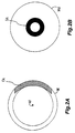
- the exposed area on the mask M of the projection optical system is an arcuate area EA outside of the optical axis AX, as shown in Fig. 2A.
- the exposed area off the axis is utilized to make the so-called "OFF ⁇ AXIS type forward/backward optical path separation".
- the primary mirror MS and the auxiliary mirror MF of the second imaging optical system K2 have the first aperture AP1 and the second aperture AP2, respectively, as described above.
- a ring-shaped shading area SA is disposed at the reflecting mirror M4 providing a pupil plane.
- the shading area SA will invite, if too large, a deterioration of the imaging performance so that it is desired to be as small as possible. Therefore, the optical system is so arranged that the emitted radiation may pass through the aperture at the image conjugate position where the opening of the luminous flux is small and that the emitted radiation may be reflected at the position, where the opening of the luminous flux is large, by the reflecting surfaces of the primary mirror MS and the auxiliary mirror MF. If the aperture is arranged at the image conjugate position, on the other hand, its effective area takes an arcuate shape. Therefore, the shading area can be reduced by forming the shading area SA in the pupil into the ring shape, as shown in Fig. 2B.
- the emitted radiation to pass through the vicinity of the center of the pupil plane can be utilized to decrease the shaded ratio of the diffracted radiation generated at the mask M but increase the ratio of interference between the 0-th degree diffracted radiation and the ⁇ first degree diffracted radiation, thereby to prevent the degradation of the contrast of the final image I2.
- the shading area SA of the convex mirror M3 near the pupil plane in the first imaging optical system K1 is desired to have the shading member arranged to shade the emitted radiation.
- the position and the size of the shading area SA can be made substantially identical with respect to the emitted radiation from the entire area of the screen.
- the imaging performance can be made substantially identical in the screen.
- this shading area SA can be formed by forming on the reflecting surface of the convex mirror M3 the reflecting area having a predetermined reflectivity and a low reflecting area having a lower reflectivity than that of the former reflecting area.
- the reflectivity of the low reflecting area is desired to be substantially zero or extremely low.
- the present projection optical system has six aspherical planes (e.g., ASP1 in lens data, as will be described hereinafter). By thus introducing the aspherical planes, the resolution can be improved.
- the projection optical system further has a field stop S1 in the vicinity of the intermediate image I1 formed by the first imaging optical system K1. This field stop S1 makes it possible to prevent the stray radiation, as generated on the side of the mask M, from reaching the wafer W.
- all the optical elements composing the present projection optical system have the reflecting surfaces.
- a shading member may be disposed in the vicinity of the optical axis AX between the primary mirror MS and the auxiliary mirror MF.
- the substrate having the reflecting surface has a linear expansion coefficient of 3 ppm/°C or less.
- ULE Trademark
- ULE Ultra Low Expansion Titanium Silicate Glass
- 5 ⁇ 10 -8 0.55ppm/C
- the projection optical system can be easily assembled or adjusted to establish a sufficient imaging performance.
- the numerical aperture of the projection optical system can be made variable by arranging an aperture stop S2 in the forward/backward optical paths between the primary mirror MS and the auxiliary mirror MF of the second imaging optical system K2.
- the various items of the projection optical system according to the first embodiment are enumerated in Table 1.
- Table 1 the numerals at the left end designate the sequences of the lens surfaces from the side of the mask M (or the first plane); letter r designates the radius of curvature of the corresponding lens surface; letter d designates the distance on the optical axis from the corresponding lens surface to a next lens surface; letter ⁇ designates the magnification of the entirety of the projection optical system; letters NA designate the numerical aperture of the wafer side (or the second plane side); and letter ⁇ designates the reference wavelength.
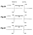
- Figs. 3A, 3B and 3C illustrate transverse aberrations (or coma-aberrations) in the meridian direction (i.e., the tangential direction) and in the sagittal direction of the projection optical system according to the present embodiment.
- the letter y designates the image height.
- the aberration diagrams of all the following embodiments use reference letters similar to those of the present embodiment.
- the aberrations are corrected in a satisfactory balance in the whole exposed area.
- the exposure wavelength on the other hand, all the wavelengths could be employed, and a sufficient resolution can be obtained even with a soft X-ray of about 13 nm.
- This coefficient k can be achieved at 0.5 or less according to the existing technical level. Therefore, a resolution of 20 nm or less can be obtained in the present embodiment.
- Fig. 4 is a diagram showing a schematic construction of a projection optical system according to a second embodiment.
- the present projection optical system is suited for the scanning type projection exposure apparatus and is constructed to include: a first imaging optical system K1 for forming two intermediate images I1 and I1' of the pattern of a mask M or a first plane; and a second imaging optical system K2 based on the emitted radiation from the intermediate image I1' for forming a final image I2 of the pattern of the mask M at a reduced magnification on a photosensitive substrate or wafer W.
- the first imaging optical system further includes: a first auxiliary imaging optical system for forming the first intermediate image I1; and a second auxiliary imaging optical system for forming the second intermediate image I1'.
- the image I1 is formed in the first imaging optical system K1.
- the present projection optical system is a teleccentric one on the wafer side, and all the optical elements composing the projection optical system have their optical axes aligned on the common straight line AX.
- the first imaging optical system K1 is constructed to include a reflecting mirror M1 of a positive power (a concave mirror), a reflecting mirror M2 of a negative power (a convex shape), reflecting mirrors M3 and M4 of positive powers (concave shapes), a reflecting mirror M5 of a negative power ( a convex shape) and a reflecting mirror M6 of a positive power (a concave shape).
- the emitted radiation as emitted from a radiation source 1, irradiates the mask and the emitted radiation from the mask M is reflected through the reflecting mirrors M1 and M2 so that the first intermediate image I1 of the pattern of the mask M is formed. And, the emitted radiation from the first intermediate image I1 is reflected sequentially through the reflecting mirrors M3 to M6 to form the second intermediate image I1'.
- the second imaging optical system K2 is constructed to include a primary mirror MS of a positive power ( a concave shape) disposed in the vicinity of the second intermediate image I1', and an auxiliary mirror MF disposed closer to the wafer W than the primary mirror MS.
- This primary mirror MS has a first aperture AP1 and a reflecting surface of a positive power ( a concave shape).
- the auxiliary mirror MF has a second aperture AP2.
- the emitted radiation from the second intermediate image I1' is reflected through the first aperture AP1 of the primary mirror MS on the reflecting surface of the auxiliary mirror MF; the emitted radiation, as reflected on the reflecting surface of the auxiliary mirror MF, is reflected on the first reflecting surface of the primary mirror MS; and the emitted radiation, as reflected on the first reflecting surface of the primary mirror MS, forms the final image I2 on the wafer W through the second aperture AP2 of the auxiliary mirror MF.
- the exposed area is an arcuate area having a radius of 17.4 to 18.0 mm on an optical axis AX, and a field size of a width of 22 mm can be used in the scanning direction, as indicated by arrow SC in Fig. 4.
- the shading area SA is formed in the reflecting mirror M1.
- the shape of the shading area and the method of separating the forward/backward optical paths in the present embodiment are similar to those of the first embodiment, and their description will be omitted.
- the OFF-AXIS type optical path separation is performed in the two, i.e., first and second auxiliary imaging optical systems
- the center shading type optical path separation is performed in the one, i.e., second imaging optical system K2.
- the invention should not be limited thereto, but may also perform the OFF-AXIS type optical path separation with one optical system and the center shading type optical separation with the two optical systems.
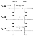
- Figs. 5A, 5B and 5C are diagrams illustrating a transverse aberration of the optical system according to the second embodiment. As apparent from Figs. 5A, 5B and 5C the aberrations are corrected in a satisfactory balance in the whole exposed area.
- the exposure wavelength on the other hand, all the wavelengths could be employed, and a sufficient resolution can be obtained even with a soft X-ray of about 13 nm. From the foregoing Formula of the resolution W, a resolution of 12 nm or higher is obtained in the present embodiment.
- Fig. 6 is a diagram showing a schematic construction of a projection optical system according to a third embodiment.
- the present projection optical system is one suited for a scanning type projection exposure apparatus.
- the projection optical system has at least one refractive lens component L1 in the first imaging optical system when an exposure radiation of 100 to 200 nm is used, and employs a transmission type mask to make the optical systems telecentric on both the sides of the mask M and the wafer W.
- the image distortion can be reduced even when the positions of the mask M and/or the wafer W are displaced in the axial direction.
- the present projection optical system TL is constructed to include: a first imaging optical system K1 for forming two intermediate images I1 and I1' of the pattern of a mask M or a first plane; and a second imaging optical system K2 based on the emitted radiation from the intermediate image I1' for forming a final image I2 of the pattern of the mask M at a reduced magnification on a photosensitive substrate or wafer W.
- the first imaging optical system K1 further includes: a first auxiliary imaging optical system for forming the first intermediate image I1; and a second auxiliary imaging optical system for forming the second intermediate image I1'.
- the image I1 is formed in the first imaging optical system K1.
- all the optical elements composing the projection optical system TL have their optical axes aligned on the common straight line AX.
- the first imaging optical system K1 is constructed to include a positive lens component L1 made of a fluorite, a reflecting mirror M1 of a positive power ( a concave shape), a reflecting mirror M2 of a negative power ( a convex shape), reflecting mirrors M3 and M4 of positive powers (concave shapes), a reflecting mirror M5 of a negative power (a convex shape) and a reflecting mirror M6 of a positive power (a concave shape).
- the emitted radiation as emitted from a radiation source 1, irradiates the mask and the emitted radiation from the mask M passes through the lens component L1 and is reflected through the reflecting mirrors M1 and M2 so that the first intermediate image I1 of the pattern of the mask M is formed. And, the emitted radiation from the first intermediate image I1 is reflected sequentially through the reflecting mirrors M3 to M6 to form the second intermediate image I1' of the pattern of the mask M.
- the second imaging optical system K2 is constructed to include a primary mirror MS of a positive power ( a concave shape) disposed in the vicinity of the second intermediate image I1', and an auxiliary mirror MF disposed closer to the wafer W than the primary mirror MS. And, this primary mirror MS has a first aperture AP1 and a reflecting surface of a positive power ( a concave shape). On the other hand, the auxiliary mirror MF has a second aperture AP2.
- the emitted radiation from the second intermediate image I1' is reflected through the first aperture AP1 of the primary mirror MS on the reflecting surface of the auxiliary mirror MF; the emitted radiation, as reflected on the reflecting surface of the auxiliary mirror MF, is reflected on the first reflecting surface of the primary mirror MS; and the emitted radiation, as reflected on the first reflecting surface of the primary mirror MS, forms the final image I2 on the wafer W through the second aperture AP2 of the auxiliary mirror MF.
- the shading area SA is provided on the reflecting mirror M1.
- the shape of the shading area and the method of separating the forward/backward optical paths in the present embodiment are similar to those of the first and second embodiments, and their description will be omitted.
- the exposed area is an arcuate area having a radius of 18.0 to 19.0 mm on an optical axis AX, and a field size of a width of 20 mm can be used in the scanning direction, as indicated by arrow SC in Fig. 6.
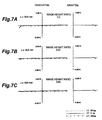
- Figs. 7A, 7B and 7C are diagrams illustrating a transverse aberration of the optical system according to the third embodiment.
- the aberrations are corrected in a satisfactory balance in the whole exposed area, as apparent from the figure.
- the fluorite i.e., calcium fluoride (CaF 2 ) is used as a material for the refractive lens component, which should not be limited to the fluorite.
- a fluoride which is preferably selected from the group consisting essentially of: the fluorite (calcium fluoride (CaF 2 ), barium fluoride (BaF 2 ), lithium fluoride (LiF), magnesium fluoride (MgF 2 ), strontium fluoride (SrF 2 ), lithium-calcium-alminium-fluoride (LiCaAlF 6 ) and lithium-strontium-aluminium-fluoride (LiSrAlF 6 ).
- a diffraction optical element may be added to the projection optical system to utilize the effect of chromatic aberration additionally by the diffraction optical element.
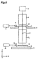
- Fig. 8 is a diagram showing a construction of a projection exposure apparatus which is provided with the projection optical systems according to the foregoing individual embodiments of the invention.
- a Z-axis is set in parallel with the optical axis AX of the projection optical system TL constructing the projection exposure apparatus;
- an X-axis is set in parallel with the sheet surface of Fig. 8 and in a plane perpendicular to the optical axis AX; and a Y-axis is set normal to the sheet surface.
- the mask M On the object place of the projection optical system TL, on the other hand, there is arranged the mask M as a projection original having a predetermined circuit pattern formed thereon.
- the wafer W On the image plane of the projection optical system TL, there is arranged the wafer W to which a photoresist is applied as the substrate.
- the emitted radiation as emitted from a radiation source 1, irradiates the mask M having the predetermined pattern homogeneously through an illumination optical system 2.
- an illumination optical system 2 On the optical path from the radiation source 1 to the illumination optical system 2, there is arranged one or a plurality of deflecting mirrors, if necessary, for changing the optical path.
- the illumination optical system 2 is constructed, for example, to include: a fly-eye lens for homogenizing the illuminance distribution of the exposure radiation; an optical integrator having an internal reflection type integrator for forming a surface illuminant having a predetermined size/shape; a variable field stop (or reticle blind) for regulating the size/shape of the illumination area on the mask M; and an optical system such as a field stop imaging optical system for projecting the image of the field stop on the mask.
- the mask M is held through a reticle holder 4 in parallel with the X-Y plane on a reticle stage 5.
- a pattern to be transferred is formed on the mask M, the pattern area of which is irradiated all over with the radiation coming from the illumination optical system 2.
- the reticle stage 5 can be moved two-dimensionally along the mask plane (i.e., the X-Y plane) by the actions of the not-shown drive system.
- the location coordinates of the reticle stage 5 are measured and positioned by an interferometer 7 using a mask carrier mirror 6.
- the radiation from the pattern formed on the mask M forms a mask pattern image through the projection optical system TL on the wafer W or the photosensitive substrate.
- the projection optical system TL is equipped, in the vicinity of its pupil position, with the aperture stop S2 (as should be referred to Fig. 1) having a variable aperture, and is made substantially telecentric on the sides of the mask M and the wafer W.
- the wafer W is held through a wafer holder 10 on a wafer stage 11 in parallel with the X-Y plane. And, the pattern image is formed in the exposure area having a shape substantially similar to the illumination area on the mask M.
- the wafer stage 11 can be moved two-dimensionally along the wafer plane (i.e., the X-Y plane) by the actions of the not-shown drive system.
- the location coordinates of the wafer stage 11 are measured and positioned by an interferometer 13 using a wafer carrier mirror 12.
- the field area (or illumination area) on the mask M and the projection area (or exposure area) on the wafer W, as defined by the projection optical system TL, are formed into rectangular shapes having a shorter side in the X-direction. Therefore, the drive systems and the interferometers (7, 13) are used to position the mask 3 and the wafer W, and the not-shown auto-focus/auto-leveling system is used to position the wafer W on the imaging plane of the projection optical system.
- the mask stage 5 and the wafer stage 11 are synchronously moved (or scanned) to scan and expose the mask pattern on the wafer W with respect to the area which has a width equal to the longer side of the exposure area and a length according to the scanning (or movement) of the wafer W.
- the embodiment of Fig. 8 adopts the step-and-scan method, but the exposure apparatus of the present embodiment may be exemplified by the stitching and slit-scan type.
- this stitching and slit-scan type is adopted, the reticle and the substrate are synchronously scanned in a predetermined first direction relative to the illumination area of a predetermined shape on the reticle, to expose the area of a first row on the substrate.
- the reticle is either replaced or moved a predetermined distance in a second direction perpendicular to the first direction of the illumination area, thereby to shift the substrate transversely in the direction conjugate with the second direction of the illumination area.
- the reticle and the substrate are synchronously scanned again in the first direction relative to the illumination area of the predetermined shape on the reticle, thereby to expose the area of a second row on the substrate.
- this stitching and slit-scan type exposure apparatus a wider area on the substrate than the exposure field of the projection optical system can be exposed to the pattern of the reticle.
- this stitching and slit-scan type exposure apparatus has been disclosed in USP No. 5,477,304, Japanese Patent Laid-Open No. 330220/1996, (corresponding to US Patent Application No. 654,747, as filed on May 29, 1996) and Japanese Patent Laid-Open Nos. 148241/1997 and 284408/1998.
- the present invention can adopt the batch exposure method by which the pattern image on the reticle is batch-transferred to a predetermined shot area on the substrate.
- Fig. 8 is provided with one wafer stage for holding the wafer as the work (or photosensitive substrate) but may be constructed to include two sets of wafer stages, as disclosed in Japanese Patent Laid-Open No. 175098/1993 and EP951054A (corresponding to US Patent Application No. 980,315, as filed on November 28, 1997).
- the SOR or laser plasma X-ray source for supplying an emitted radiation (of soft X-ray) having a wavelength of about 13 nm.
- the wavelength per se is not restricted because of the cataptric optical system. This makes it possible to use a hard X-ray of about 1 nm, a radiation of a wavelength of about 26 nm or about 39 nm, an ultraviolet radiation (light) such as the g-line or i-line, a deep ultraviolet (DUV) radiation such as the radiation from the KeF excimer laser, the F 2 laser or Kr 2 laser.
- a reflection type mask is used as the reticle (projection original), and reflection optical members is used as optical members in the illumination optical system.
- the third embodiment has a refractive member so that it can use an ultraviolet radiation such as the g-line and i-line, a deep ultraviolet (DUV) radiation such as the KrF excimer laser, or a vacuum ultraviolet (VUV) radiation such as the ArF excimer laser, the F 2 laser, the Kr 2 laser or the Ar 2 laser.
- the radiation source may be exemplified by higher harmonics of the solid laser such as the YAG laser having an oscillatory spectrum at any of the wavelengths of 248 nm, 193 nm, 157 nm, 146 nm and 126 nm.
- the optical path from the mask (or first plane) to the wafer (or second plane) is in the vacuum atmosphere.
- the optical path from the mask (or first plane) to the wafer (or second plane) is replaced by the helium gas atmosphere.
- the projection optical system may have a multiplying factor not only for reduction but also for equalization or magnification.
- the invention can be applied not only to an exposure apparatus to be used for manufacturing semiconductor elements but also an exposure apparatus for transferring a device pattern to a glass plate, as used for manufacturing a display including a liquid crystal element, an exposure apparatus for transferring a device pattern to a ceramics wafer, as used for manufacturing a thin-film magnetic head, and an exposure apparatus to be used for manufacturing an imaging element (e.g., CCD).
- the invention can also be applied to an exposure apparatus for transferring a circuit pattern to a glass substrate or a silicon wafer so as to manufacture the reticle or mask.
- a metal film is evapolated on the wafers of one lot at Step 301 of Fig. 9.
- a photoresist is applied to the metal films on the wafers of the lot.
- the projection exposure apparatus of Fig. 8 as provided with the projection optical system TL of any of the first to third embodiments, is used to expose and transfer the images of the pattern of a reticle R sequentially through the projection optical system TL to the individual shot areas on the wafers of the lot.
- the photoresists on the wafers of the lot are developed.
- the wafers of the lot are etched by using the resist pattern as the mask so that the circuit pattern corresponding to the pattern on the reticle R is formed in each shot area on each wafer.
- the circuit pattern of the overlying layer is formed to manufacture the device such as the semiconductor element.
- the projection optical system of the invention As has been described hereinbefore, it is possible to provide a projection optical system which has a large numerical aperture in a soft X-ray wavelength range of 200 nm or less, especially 100 nm or less and which has a resolution far smaller than 50 nm.
- the projection exposure apparatus according to the invention is provided with the projection optical system so that it can manufacture devices having fine patterns.
Applications Claiming Priority (2)
| Application Number | Priority Date | Filing Date | Title |
|---|---|---|---|
| JP29422499 | 1999-10-15 | ||
| JP29422499 | 1999-10-15 |
Publications (2)
| Publication Number | Publication Date |
|---|---|
| EP1093021A2 true EP1093021A2 (fr) | 2001-04-18 |
| EP1093021A3 EP1093021A3 (fr) | 2004-06-30 |
Family
ID=17804955
Family Applications (1)
| Application Number | Title | Priority Date | Filing Date |
|---|---|---|---|
| EP00122217A Withdrawn EP1093021A3 (fr) | 1999-10-15 | 2000-10-16 | Système d'exposition par projection, ainsi qu'un appareil et des méthodes utilisant ce système |
Country Status (2)
| Country | Link |
|---|---|
| US (1) | US6750948B2 (fr) |
| EP (1) | EP1093021A3 (fr) |
Cited By (23)
| Publication number | Priority date | Publication date | Assignee | Title |
|---|---|---|---|---|
| EP1209503A2 (fr) * | 2000-11-07 | 2002-05-29 | Asm Lithography B.V. | Dispositif de lithographie et méthode de production d'un dispositif |
| WO2003016977A2 (fr) * | 2001-08-16 | 2003-02-27 | Carl Zeiss Smt Ag | Objectif a obscurcissement des pupilles |
| US6710917B2 (en) | 2000-10-20 | 2004-03-23 | Carl Zeiss Smt Ag | 8-mirror microlithography projection objective |
| WO2004046771A1 (fr) * | 2002-11-21 | 2004-06-03 | Carl Zeiss Smt Ag | Lentille de projection dotee d'un diaphragme de forme non circulaire pour microlithographie |
| EP1597630A1 (fr) * | 2003-02-28 | 2005-11-23 | Micronic Laser Systems Ab | Scripteur direct par modulation spatiale de lumiere |
| KR100588112B1 (ko) * | 2000-11-07 | 2006-06-09 | 에이에스엠엘 네델란즈 비.브이. | 리소그래피장치, 디바이스 제조방법 및 그 디바이스 |
| WO2006069725A1 (fr) * | 2004-12-23 | 2006-07-06 | Carl Zeiss Smt Ag | Objectif a grande ouverture et pupille obscurcie |
| EP1950594A1 (fr) | 2007-01-17 | 2008-07-30 | Carl Zeiss SMT AG | Système optique, installation d'éclairage à projection pour la microlithographie dotée d'une telle système optique, procédé de fabrication d'un composant microstructuré à l'aide d'une telle installation d'éclairage à projection, composant microstructuré fabriqué selon ce procédé de fabrication, ainsi qu'utilisation d'une telle système optique |
| WO2009121541A1 (fr) * | 2008-04-04 | 2009-10-08 | Carl Zeiss Smt Ag | Dispositif d'éclairage microlithographique par projection, et dispositif d'inspection d'une surface d'un substrat |
| WO2010006678A1 (fr) | 2008-07-16 | 2010-01-21 | Carl Zeiss Smt Ag | Optique d'imagerie |
| DE102008046699A1 (de) | 2008-09-10 | 2010-03-11 | Carl Zeiss Smt Ag | Abbildende Optik |
| US7682031B2 (en) | 2004-12-23 | 2010-03-23 | Carl Zeiss Smt Ag | Catoptric objectives and systems using catoptric objectives |
| DE102009025656A1 (de) | 2008-09-17 | 2010-04-15 | Carl Zeiss Smt Ag | Projektionsoptik zur Verwendung in einer Mikrolithographie-Projektionsbelichtungsanlage mit einer Blende |
| WO2010149487A2 (fr) | 2009-06-24 | 2010-12-29 | Carl Zeiss Smt Gmbh | Système optique dimagerie pour imager un champ dobjet dans un champ dimage, et système optique déclairage pour éclairer un champ dobjet |
| US7869138B2 (en) | 2006-03-27 | 2011-01-11 | Carl Zeiss Smt Ag | Projection objective and projection exposure apparatus with negative back focus of the entry pupil |
| CN102378935A (zh) * | 2009-03-30 | 2012-03-14 | 卡尔蔡司Smt有限责任公司 | 成像光学部件以及具有此类型的成像光学部件的用于微光刻的投射曝光装置 |
| US8169694B2 (en) | 2005-09-13 | 2012-05-01 | Carl Zeiss Smt Gmbh | Catoptric objectives and systems using catoptric objectives |
| US8411251B2 (en) | 2006-12-28 | 2013-04-02 | Carl Zeiss Smt Gmbh | Optical element and illumination optics for microlithography |
| US8576376B2 (en) | 2007-10-26 | 2013-11-05 | Carl Zeiss Smt Gmbh | Imaging optical system and projection exposure system for microlithography |
| US8605255B2 (en) | 2007-10-26 | 2013-12-10 | Carl Zeiss Smt Gmbh | Imaging optical system and projection exposure system including the same |
| US8610877B2 (en) | 2009-02-12 | 2013-12-17 | Carl Zeiss Smt Gmbh | Imaging optical system and projection exposure installation for microlithography with an imaging optical system of this type |
| US8705005B2 (en) | 2006-02-17 | 2014-04-22 | Carl Zeiss Smt Gmbh | Microlithographic illumination system |
| US8717538B2 (en) | 2007-10-26 | 2014-05-06 | Carl Zeiss Smt Gmbh | Catoptric imaging optical system with an arc-shaped object field |
Families Citing this family (32)
| Publication number | Priority date | Publication date | Assignee | Title |
|---|---|---|---|---|
| TW538256B (en) * | 2000-01-14 | 2003-06-21 | Zeiss Stiftung | Microlithographic reduction projection catadioptric objective |
| JP2004512552A (ja) * | 2000-10-20 | 2004-04-22 | カール ツァイス シュティフトゥング トレイディング アズ カール ツァイス | 8反射鏡型マイクロリソグラフィ用投影光学系 |
| JP4245286B2 (ja) * | 2000-10-23 | 2009-03-25 | 株式会社ニコン | 反射屈折光学系および該光学系を備えた露光装置 |
| JP2003045782A (ja) | 2001-07-31 | 2003-02-14 | Canon Inc | 反射型縮小投影光学系及びそれを用いた露光装置 |
| DE10220324A1 (de) * | 2002-04-29 | 2003-11-13 | Zeiss Carl Smt Ag | Projektionsverfahren mit Pupillenfilterung und Projektionsobjektiv hierfür |
| US7348575B2 (en) | 2003-05-06 | 2008-03-25 | Nikon Corporation | Projection optical system, exposure apparatus, and exposure method |
| KR101516142B1 (ko) | 2003-05-06 | 2015-05-04 | 가부시키가이샤 니콘 | 투영 광학계, 노광 장치 및 노광 방법 |
| US8208198B2 (en) | 2004-01-14 | 2012-06-26 | Carl Zeiss Smt Gmbh | Catadioptric projection objective |
| US7466489B2 (en) | 2003-12-15 | 2008-12-16 | Susanne Beder | Projection objective having a high aperture and a planar end surface |
| JP5102492B2 (ja) | 2003-12-19 | 2012-12-19 | カール・ツァイス・エスエムティー・ゲーエムベーハー | 結晶素子を有するマイクロリソグラフィー投影用対物レンズ |
| DE602005008707D1 (de) * | 2004-01-14 | 2008-09-18 | Zeiss Carl Smt Ag | Catadioptrisches projektionsobjektiv |
| US20080151365A1 (en) | 2004-01-14 | 2008-06-26 | Carl Zeiss Smt Ag | Catadioptric projection objective |
| US7463422B2 (en) * | 2004-01-14 | 2008-12-09 | Carl Zeiss Smt Ag | Projection exposure apparatus |
| US7712905B2 (en) | 2004-04-08 | 2010-05-11 | Carl Zeiss Smt Ag | Imaging system with mirror group |
| JP2005317611A (ja) * | 2004-04-27 | 2005-11-10 | Canon Inc | 露光方法及び装置 |
| KR20170129271A (ko) | 2004-05-17 | 2017-11-24 | 칼 짜이스 에스엠티 게엠베하 | 중간이미지를 갖는 카타디옵트릭 투사 대물렌즈 |
| JP4711437B2 (ja) * | 2004-06-23 | 2011-06-29 | 株式会社ニコン | 投影光学系、露光装置および露光方法 |
| US7312851B2 (en) * | 2004-06-23 | 2007-12-25 | Nikon Corporation | Projection optical system, exposure apparatus, and exposure method in which a reflective projection optical system has a non-circular aperture stop |
| US20060138349A1 (en) * | 2004-12-27 | 2006-06-29 | Asml Netherlands B.V. | Lithographic apparatus and device manufacturing method |
| KR100674959B1 (ko) * | 2005-02-23 | 2007-01-26 | 삼성전자주식회사 | 비축상 프로젝션 광학계 및 이를 적용한 극자외선 리소그래피 장치 |
| JP2006245147A (ja) * | 2005-03-01 | 2006-09-14 | Canon Inc | 投影光学系、露光装置及びデバイスの製造方法 |
| EP1856578B1 (fr) * | 2005-03-08 | 2010-05-19 | Carl Zeiss SMT AG | Systeme de projection pour microlithographie a diaphragme accessible ou butee d'ouverture |
| US20090115986A1 (en) * | 2005-06-02 | 2009-05-07 | Carl Zeiss Smt Ag | Microlithography projection objective |
| US7626181B2 (en) * | 2005-12-09 | 2009-12-01 | Asml Netherlands B.V. | Lithographic apparatus and device manufacturing method |
| US20080118849A1 (en) * | 2006-11-21 | 2008-05-22 | Manish Chandhok | Reflective optical system for a photolithography scanner field projector |
| US7929114B2 (en) | 2007-01-17 | 2011-04-19 | Carl Zeiss Smt Gmbh | Projection optics for microlithography |
| KR101433424B1 (ko) * | 2007-09-21 | 2014-08-26 | 칼 짜이스 에스엠티 게엠베하 | 마이크로리소그래피용 엄폐 퓨필을 가진 투사 대물렌즈 |
| CN102341738B (zh) | 2009-03-06 | 2015-11-25 | 卡尔蔡司Smt有限责任公司 | 成像光学部件以及具有该类型成像光学部件的用于微光刻的投射曝光装置 |
| DE102009046685A1 (de) | 2009-11-13 | 2011-05-26 | Carl Zeiss Smt Gmbh | Abbildende Optik |
| DE102011006468B4 (de) | 2011-03-31 | 2014-08-28 | Carl Zeiss Smt Gmbh | Vermessung eines abbildenden optischen Systems durch Überlagerung von Mustern |
| DE102012208793A1 (de) | 2012-05-25 | 2013-11-28 | Carl Zeiss Smt Gmbh | Abbildende Optik sowie Projektionsbelichtungsanlage für die Projektionslithographie mit einer derartigen abbildenden Optik |
| DE102012218558A1 (de) | 2012-10-11 | 2013-08-29 | Carl Zeiss Smt Gmbh | Abbildende Optik sowie Projektionsbelichtungsanlage für die Projektionslithographie mit einer derartigen abbildenden Optik |
Citations (3)
| Publication number | Priority date | Publication date | Assignee | Title |
|---|---|---|---|---|
| US3911781A (en) | 1972-11-21 | 1975-10-14 | Upat Max Langensiepen Kg | Anchor sleeve for use in bores formed in relatively easily friable materials |
| FR2530306A1 (fr) | 1982-07-16 | 1984-01-20 | Brechet Michel | Vis autoperceuse, autotaraudeuse, demontable, et sa mise en oeuvre |
| EP0501201A1 (fr) | 1991-02-28 | 1992-09-02 | ALLFA DÜBEL GmbH | Ensemble d'éléments pour le vissage de chevilles dans un matériau poreux |
Family Cites Families (35)
| Publication number | Priority date | Publication date | Assignee | Title |
|---|---|---|---|---|
| US4812028A (en) * | 1984-07-23 | 1989-03-14 | Nikon Corporation | Reflection type reduction projection optical system |
| EP0947882B1 (fr) | 1986-07-11 | 2006-03-29 | Canon Kabushiki Kaisha | Système d'exposition, par projection en réduction, de rayons X, du type réflectif |
| US4913524A (en) * | 1988-05-12 | 1990-04-03 | The Perkin-Elmer Corporation | Synthetic imaging technique |
| US5063586A (en) | 1989-10-13 | 1991-11-05 | At&T Bell Laboratories | Apparatus for semiconductor lithography |
| US5315629A (en) * | 1990-10-10 | 1994-05-24 | At&T Bell Laboratories | Ringfield lithography |
| US5212588A (en) * | 1991-04-09 | 1993-05-18 | The United States Of America As Represented By The United States Department Of Energy | Reflective optical imaging system for extreme ultraviolet wavelengths |
| JP3203719B2 (ja) | 1991-12-26 | 2001-08-27 | 株式会社ニコン | 露光装置、その露光装置により製造されるデバイス、露光方法、およびその露光方法を用いたデバイス製造方法 |
| US5220590A (en) | 1992-05-05 | 1993-06-15 | General Signal Corporation | X-ray projection lithography camera |
| US5353322A (en) | 1992-05-05 | 1994-10-04 | Tropel Corporation | Lens system for X-ray projection lithography camera |
| US5477304A (en) | 1992-10-22 | 1995-12-19 | Nikon Corporation | Projection exposure apparatus |
| US6078381A (en) | 1993-02-01 | 2000-06-20 | Nikon Corporation | Exposure method and apparatus |
| US5410434A (en) | 1993-09-09 | 1995-04-25 | Ultratech Stepper, Inc. | Reflective projection system comprising four spherical mirrors |
| US5488229A (en) * | 1994-10-04 | 1996-01-30 | Excimer Laser Systems, Inc. | Deep ultraviolet microlithography system |
| JP3711586B2 (ja) | 1995-06-02 | 2005-11-02 | 株式会社ニコン | 走査露光装置 |
| US5805365A (en) | 1995-10-12 | 1998-09-08 | Sandia Corporation | Ringfield lithographic camera |
| JP3456323B2 (ja) | 1995-11-01 | 2003-10-14 | 株式会社ニコン | 顕微鏡対物レンズ |
| JPH09148241A (ja) | 1995-11-27 | 1997-06-06 | Canon Inc | 走査露光装置及びそれを用いたデバイスの製造方法 |
| US5815310A (en) | 1995-12-12 | 1998-09-29 | Svg Lithography Systems, Inc. | High numerical aperture ring field optical reduction system |
| JPH09251097A (ja) | 1996-03-15 | 1997-09-22 | Nikon Corp | X線リソグラフィー用反射縮小結像光学系 |
| US5686728A (en) | 1996-05-01 | 1997-11-11 | Lucent Technologies Inc | Projection lithography system and method using all-reflective optical elements |
| AU5067898A (en) | 1996-11-28 | 1998-06-22 | Nikon Corporation | Aligner and method for exposure |
| JPH10284408A (ja) | 1997-04-08 | 1998-10-23 | Nikon Corp | 露光方法 |
| US5956192A (en) | 1997-09-18 | 1999-09-21 | Svg Lithography Systems, Inc. | Four mirror EUV projection optics |
| US6199991B1 (en) | 1997-11-13 | 2001-03-13 | U.S. Philips Corporation | Mirror projection system for a scanning lithographic projection apparatus, and lithographic apparatus comprising such a system |
| US5920380A (en) | 1997-12-19 | 1999-07-06 | Sandia Corporation | Apparatus and method for generating partially coherent illumination for photolithography |
| US6014252A (en) | 1998-02-20 | 2000-01-11 | The Regents Of The University Of California | Reflective optical imaging system |
| US6396067B1 (en) | 1998-05-06 | 2002-05-28 | Koninklijke Philips Electronics N.V. | Mirror projection system for a scanning lithographic projection apparatus, and lithographic apparatus comprising such a system |
| DE19923609A1 (de) | 1998-05-30 | 1999-12-02 | Zeiss Carl Fa | Ringfeld-4-Spiegelsysteme mit konvexem Primärspiegel für die EUV-Lithographie |
| EP0964307A3 (fr) | 1998-06-08 | 2001-09-05 | Nikon Corporation | Dispositif et méthode d' exposition par projection |
| US6213610B1 (en) * | 1998-09-21 | 2001-04-10 | Nikon Corporation | Catoptric reduction projection optical system and exposure apparatus and method using same |
| JP2000100694A (ja) * | 1998-09-22 | 2000-04-07 | Nikon Corp | 反射縮小投影光学系、該光学系を備えた投影露光装置および該装置を用いた露光方法 |
| EP1035445B1 (fr) * | 1999-02-15 | 2007-01-31 | Carl Zeiss SMT AG | Objectif de réduction pour la microlithographie et appareil d' exposition par projection |
| US6033079A (en) | 1999-03-15 | 2000-03-07 | Hudyma; Russell | High numerical aperture ring field projection system for extreme ultraviolet lithography |
| US6188513B1 (en) * | 1999-03-15 | 2001-02-13 | Russell Hudyma | High numerical aperture ring field projection system for extreme ultraviolet lithography |
| US6285737B1 (en) | 2000-01-21 | 2001-09-04 | Euv Llc | Condenser for extreme-UV lithography with discharge source |
-
2000
- 2000-10-16 EP EP00122217A patent/EP1093021A3/fr not_active Withdrawn
-
2002
- 2002-03-25 US US10/104,033 patent/US6750948B2/en not_active Expired - Fee Related
Patent Citations (3)
| Publication number | Priority date | Publication date | Assignee | Title |
|---|---|---|---|---|
| US3911781A (en) | 1972-11-21 | 1975-10-14 | Upat Max Langensiepen Kg | Anchor sleeve for use in bores formed in relatively easily friable materials |
| FR2530306A1 (fr) | 1982-07-16 | 1984-01-20 | Brechet Michel | Vis autoperceuse, autotaraudeuse, demontable, et sa mise en oeuvre |
| EP0501201A1 (fr) | 1991-02-28 | 1992-09-02 | ALLFA DÜBEL GmbH | Ensemble d'éléments pour le vissage de chevilles dans un matériau poreux |
Cited By (66)
| Publication number | Priority date | Publication date | Assignee | Title |
|---|---|---|---|---|
| US6710917B2 (en) | 2000-10-20 | 2004-03-23 | Carl Zeiss Smt Ag | 8-mirror microlithography projection objective |
| EP1209503A2 (fr) * | 2000-11-07 | 2002-05-29 | Asm Lithography B.V. | Dispositif de lithographie et méthode de production d'un dispositif |
| KR100588112B1 (ko) * | 2000-11-07 | 2006-06-09 | 에이에스엠엘 네델란즈 비.브이. | 리소그래피장치, 디바이스 제조방법 및 그 디바이스 |
| EP2081086A3 (fr) * | 2000-11-07 | 2010-03-24 | ASML Netherlands B.V. | Appareil lithographique et procédé de fabrication du dispositif |
| EP1679550A1 (fr) * | 2000-11-07 | 2006-07-12 | ASML Netherlands B.V. | Appareil lithographique et procédé de fabrication du dispositif |
| EP1209503A3 (fr) * | 2000-11-07 | 2004-07-28 | ASML Netherlands B.V. | Dispositif de lithographie et méthode de production d'un dispositif |
| US8967817B2 (en) | 2001-05-25 | 2015-03-03 | Carl Zeiss Smt Gmbh | Imaging optical system with at most 11.6% of the illuminated surfaces of the pupil plane being obscured |
| US6894834B2 (en) | 2001-08-16 | 2005-05-17 | Carl Zeiss Smt Ag | Objective with pupil obscuration |
| WO2003016977A3 (fr) * | 2001-08-16 | 2003-12-04 | Zeiss Carl Smt Ag | Objectif a obscurcissement des pupilles |
| US7209286B2 (en) | 2001-08-16 | 2007-04-24 | Carl Zeiss Smt Ag | Objective with pupil obscuration |
| WO2003016977A2 (fr) * | 2001-08-16 | 2003-02-27 | Carl Zeiss Smt Ag | Objectif a obscurcissement des pupilles |
| WO2004046771A1 (fr) * | 2002-11-21 | 2004-06-03 | Carl Zeiss Smt Ag | Lentille de projection dotee d'un diaphragme de forme non circulaire pour microlithographie |
| US7221516B2 (en) | 2002-11-21 | 2007-05-22 | Carl Zeiss Smt Ag | Projection lens for a microlithographic projection exposure apparatus |
| CN100399063C (zh) * | 2002-11-21 | 2008-07-02 | 卡尔蔡司Smt股份有限公司 | 带非圆形光阑的微印刷用投影镜头 |
| EP1597630A1 (fr) * | 2003-02-28 | 2005-11-23 | Micronic Laser Systems Ab | Scripteur direct par modulation spatiale de lumiere |
| US9304407B2 (en) | 2004-12-23 | 2016-04-05 | Carl Zeiss Smt Gmbh | Catoptric objectives and systems using catoptric objectives |
| CN101713864B (zh) * | 2004-12-23 | 2013-10-30 | 卡尔蔡司Smt有限责任公司 | 具有暗化光瞳的大孔径物镜 |
| KR101306438B1 (ko) * | 2004-12-23 | 2013-09-09 | 칼 짜이스 에스엠티 게엠베하 | 차폐된 동공을 가진 렌즈 |
| US7682031B2 (en) | 2004-12-23 | 2010-03-23 | Carl Zeiss Smt Ag | Catoptric objectives and systems using catoptric objectives |
| US8317345B2 (en) | 2004-12-23 | 2012-11-27 | Carl Zeiss Smt Gmbh | Catoptric objectives and systems using catoptric objectives |
| KR101306355B1 (ko) * | 2004-12-23 | 2013-09-09 | 칼 짜이스 에스엠티 게엠베하 | 차폐된 동공을 가진 렌즈 |
| WO2006069725A1 (fr) * | 2004-12-23 | 2006-07-06 | Carl Zeiss Smt Ag | Objectif a grande ouverture et pupille obscurcie |
| KR101306346B1 (ko) * | 2004-12-23 | 2013-09-09 | 칼 짜이스 에스엠티 게엠베하 | 차폐된 동공을 가진 렌즈 |
| KR101306499B1 (ko) * | 2004-12-23 | 2013-09-09 | 칼 짜이스 에스엠티 게엠베하 | 차폐된 동공을 가진 렌즈 |
| US8004755B2 (en) | 2004-12-23 | 2011-08-23 | Carl Zeiss Smt Gmbh | Catoptric objectives and systems using catoptric objectives |
| US8632195B2 (en) | 2004-12-23 | 2014-01-21 | Carl Zeiss Smt Gmbh | Catoptric objectives and systems using catoptric objectives |
| US8169694B2 (en) | 2005-09-13 | 2012-05-01 | Carl Zeiss Smt Gmbh | Catoptric objectives and systems using catoptric objectives |
| US9465300B2 (en) | 2005-09-13 | 2016-10-11 | Carl Zeiss Smt Gmbh | Catoptric objectives and systems using catoptric objectives |
| US8705005B2 (en) | 2006-02-17 | 2014-04-22 | Carl Zeiss Smt Gmbh | Microlithographic illumination system |
| US9341953B2 (en) | 2006-02-17 | 2016-05-17 | Carl Zeiss Smt Gmbh | Microlithographic illumination system |
| US8094380B2 (en) | 2006-03-27 | 2012-01-10 | Carl Zeiss Smt Gmbh | Projection objective and projection exposure apparatus with negative back focus of the entry pupil |
| US7869138B2 (en) | 2006-03-27 | 2011-01-11 | Carl Zeiss Smt Ag | Projection objective and projection exposure apparatus with negative back focus of the entry pupil |
| US8810927B2 (en) | 2006-03-27 | 2014-08-19 | Carl Zeiss Smt Gmbh | Projection objective and projection exposure apparatus with negative back focus of the entry pupil |
| US8411251B2 (en) | 2006-12-28 | 2013-04-02 | Carl Zeiss Smt Gmbh | Optical element and illumination optics for microlithography |
| US8810903B2 (en) | 2007-01-17 | 2014-08-19 | Carl Zeiss Smt Gmbh | Imaging optical system |
| US8018650B2 (en) | 2007-01-17 | 2011-09-13 | Carl Zeiss Smt Gmbh | Imaging optical system |
| US8208200B2 (en) | 2007-01-17 | 2012-06-26 | Carl Zeiss Smt Gmbh | Imaging optical system |
| US9298100B2 (en) | 2007-01-17 | 2016-03-29 | Carl Zeiss Smt Gmbh | Imaging optical system |
| EP1950594A1 (fr) | 2007-01-17 | 2008-07-30 | Carl Zeiss SMT AG | Système optique, installation d'éclairage à projection pour la microlithographie dotée d'une telle système optique, procédé de fabrication d'un composant microstructuré à l'aide d'une telle installation d'éclairage à projection, composant microstructuré fabriqué selon ce procédé de fabrication, ainsi qu'utilisation d'une telle système optique |
| US8576376B2 (en) | 2007-10-26 | 2013-11-05 | Carl Zeiss Smt Gmbh | Imaging optical system and projection exposure system for microlithography |
| US8605255B2 (en) | 2007-10-26 | 2013-12-10 | Carl Zeiss Smt Gmbh | Imaging optical system and projection exposure system including the same |
| US8717538B2 (en) | 2007-10-26 | 2014-05-06 | Carl Zeiss Smt Gmbh | Catoptric imaging optical system with an arc-shaped object field |
| US9285515B2 (en) | 2007-10-26 | 2016-03-15 | Carl Zeiss Smt Gmbh | Imaging optical system and projection exposure system including the same |
| US9152056B2 (en) | 2007-10-26 | 2015-10-06 | Carl Zeiss Smt Gmbh | Imaging optical system and projection exposure system for microlithography |
| WO2009121541A1 (fr) * | 2008-04-04 | 2009-10-08 | Carl Zeiss Smt Ag | Dispositif d'éclairage microlithographique par projection, et dispositif d'inspection d'une surface d'un substrat |
| US8953173B2 (en) | 2008-04-04 | 2015-02-10 | Carl Zeiss Smt Gmbh | Apparatus for microlithographic projection exposure and apparatus for inspecting a surface of a substrate |
| CN104122761B (zh) * | 2008-04-04 | 2017-11-14 | 卡尔蔡司Smt有限责任公司 | 用于微光刻投射曝光的设备以及用于检查基底表面的设备 |
| US8345267B2 (en) | 2008-04-04 | 2013-01-01 | Carl Zeiss Smt Gmbh | Apparatus for microlithographic projection exposure and apparatus for inspecting a surface of a substrate |
| CN104122761A (zh) * | 2008-04-04 | 2014-10-29 | 卡尔蔡司Smt有限责任公司 | 用于微光刻投射曝光的设备以及用于检查基底表面的设备 |
| US9442386B2 (en) | 2008-07-16 | 2016-09-13 | Carl Zeiss Smt Gmbh | Imaging optics |
| WO2010006678A1 (fr) | 2008-07-16 | 2010-01-21 | Carl Zeiss Smt Ag | Optique d'imagerie |
| US9195145B2 (en) | 2008-09-10 | 2015-11-24 | Carl Zeiss Smt Gmbh | Microlithographic imaging optical system including multiple mirrors |
| US8873122B2 (en) | 2008-09-10 | 2014-10-28 | Carl Zeiss Smt Gmbh | Microlithographic imaging optical system including multiple mirrors |
| DE102008046699A1 (de) | 2008-09-10 | 2010-03-11 | Carl Zeiss Smt Ag | Abbildende Optik |
| DE102008046699B4 (de) * | 2008-09-10 | 2014-03-13 | Carl Zeiss Smt Gmbh | Abbildende Optik |
| DE102009025656A1 (de) | 2008-09-17 | 2010-04-15 | Carl Zeiss Smt Ag | Projektionsoptik zur Verwendung in einer Mikrolithographie-Projektionsbelichtungsanlage mit einer Blende |
| US10481500B2 (en) | 2009-02-12 | 2019-11-19 | Carl Zeiss Smt Gmbh | Imaging optical system and projection exposure installation for microlithography with an imaging optical system of this type |
| US9500958B2 (en) | 2009-02-12 | 2016-11-22 | Carl Zeiss Smt Gmbh | Imaging optical system and projection exposure installation for microlithography with an imaging optical system of this type |
| US8610877B2 (en) | 2009-02-12 | 2013-12-17 | Carl Zeiss Smt Gmbh | Imaging optical system and projection exposure installation for microlithography with an imaging optical system of this type |
| CN102378935B (zh) * | 2009-03-30 | 2013-11-06 | 卡尔蔡司Smt有限责任公司 | 成像光学部件以及具有此类型的成像光学部件的用于微光刻的投射曝光装置 |
| CN102378935A (zh) * | 2009-03-30 | 2012-03-14 | 卡尔蔡司Smt有限责任公司 | 成像光学部件以及具有此类型的成像光学部件的用于微光刻的投射曝光装置 |
| US9182578B2 (en) | 2009-06-24 | 2015-11-10 | Carl Zeiss Smt Gmbh | Imaging optical system and illumination optical system |
| WO2010149487A3 (fr) * | 2009-06-24 | 2011-02-17 | Carl Zeiss Smt Gmbh | Système optique dimagerie pour imager un champ dobjet dans un champ dimage, et système optique déclairage pour éclairer un champ dobjet |
| WO2010149487A2 (fr) | 2009-06-24 | 2010-12-29 | Carl Zeiss Smt Gmbh | Système optique dimagerie pour imager un champ dobjet dans un champ dimage, et système optique déclairage pour éclairer un champ dobjet |
| CN102483516A (zh) * | 2009-06-24 | 2012-05-30 | 卡尔蔡司Smt有限责任公司 | 在像场中成像物场的成像光学系统和照明物场的照明光学系统 |
| CN102483516B (zh) * | 2009-06-24 | 2015-09-30 | 卡尔蔡司Smt有限责任公司 | 在像场中成像物场的成像光学系统和照明物场的照明光学系统 |
Also Published As
| Publication number | Publication date |
|---|---|
| US20020176063A1 (en) | 2002-11-28 |
| EP1093021A3 (fr) | 2004-06-30 |
| US6750948B2 (en) | 2004-06-15 |
Similar Documents
| Publication | Publication Date | Title |
|---|---|---|
| US6750948B2 (en) | Projection optical system, projection exposure apparatus having the projection optical system, projection method thereof, exposure method thereof and fabricating method for fabricating a device using the projection exposure apparatus | |
| JP4717974B2 (ja) | 反射屈折光学系及び該光学系を備える投影露光装置 | |
| JP2001185480A (ja) | 投影光学系及び該光学系を備える投影露光装置 | |
| KR100387003B1 (ko) | 투영광학시스템,투영노광장치,노광방법,및노광장치제조방법 | |
| KR100554784B1 (ko) | 캐터옵트릭형 투영 광학계, 노광 장치 및 디바이스의제조방법 | |
| US6819403B2 (en) | Illumination optical system, exposure apparatus, and microdevice manufacturing method | |
| US6912094B2 (en) | Projection optical system, a projection exposure apparatus, and a projection exposure method | |
| US6844915B2 (en) | Optical system and exposure apparatus provided with the optical system | |
| US20040189965A1 (en) | Projection optical system and exposure device having the projection optical system | |
| KR100587625B1 (ko) | 반사형 투영 광학계, 그것을 사용한 노광장치, 및 디바이스 제조방법 | |
| EP1079253A1 (fr) | Appareil et procede d'exposition a projection, et systeme optique reflechissant a refraction | |
| JP2002323652A (ja) | 投影光学系,該投影光学系を備えた投影露光装置および投影露光方法 | |
| EP1335229A1 (fr) | Système optique de projection du type réfléchissant, appareil d'exposition et méthode de fabrication utilisant le même | |
| US6947121B2 (en) | Projection optical system, a projection exposure apparatus provided with the same, as well as a device manufacturing method | |
| JP2004317534A (ja) | 反射屈折型の結像光学系、露光装置、および露光方法 | |
| EP1413908A2 (fr) | Système de projection optique et appareil d'exposition l'utilisant | |
| JP3239881B2 (ja) | 光学系及びそれを用いた投影装置 | |
| US6862078B2 (en) | Projection optical system and exposure apparatus with the same | |
| EP1316832A1 (fr) | Systeme optique d'image a relais et dispositif optique d'eclairage, et systeme d'exposition dote de ce systeme optique | |
| EP1418468A2 (fr) | Système optique de projection et appareil d'exposition | |
| KR20010049550A (ko) | 투영광학계 및 이것을 가진 투영노광장치, 그리고디바이스제조방법 | |
| EP1471389B1 (fr) | Système de projection optique | |
| JP2006184709A (ja) | 結像光学系、露光装置及びマイクロデバイスの製造方法 | |
| US7154586B2 (en) | Catoptric projection optical system and exposure apparatus having the same | |
| JPS61129828A (ja) | 投影露光装置 |
Legal Events
| Date | Code | Title | Description |
|---|---|---|---|
| PUAI | Public reference made under article 153(3) epc to a published international application that has entered the european phase |
Free format text: ORIGINAL CODE: 0009012 |
|
| AK | Designated contracting states |
Kind code of ref document: A2 Designated state(s): AT BE CH CY DE DK ES FI FR GB GR IE IT LI LU MC NL PT SE |
|
| AX | Request for extension of the european patent |
Free format text: AL;LT;LV;MK;RO;SI |
|
| PUAL | Search report despatched |
Free format text: ORIGINAL CODE: 0009013 |
|
| AK | Designated contracting states |
Kind code of ref document: A3 Designated state(s): AT BE CH CY DE DK ES FI FR GB GR IE IT LI LU MC NL PT SE |
|
| AX | Request for extension of the european patent |
Extension state: AL LT LV MK RO SI |
|
| 17P | Request for examination filed |
Effective date: 20041216 |
|
| AKX | Designation fees paid |
Designated state(s): AT BE CH CY DE DK ES FI FR GB GR IE IT LI LU MC NL PT SE |
|
| STAA | Information on the status of an ep patent application or granted ep patent |
Free format text: STATUS: THE APPLICATION IS DEEMED TO BE WITHDRAWN |
|
| 18D | Application deemed to be withdrawn |
Effective date: 20051201 |